LG 32LS3500 Service Manual
Hide thumbs
Also See for 32LS3500:
- Owner's manual (80 pages) ,
- User manual (74 pages) ,
- Specifications (2 pages)
Advertisement
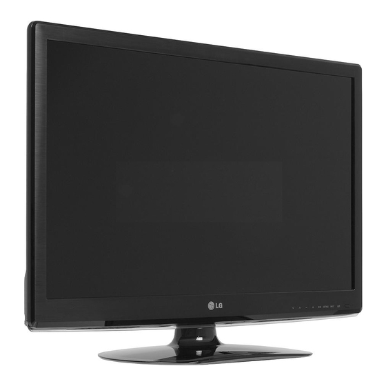
LED LCD TV
SERVICE MANUAL
CHASSIS : LC21C
MODEL : 32LS3500
MODEL :
CAUTION
BEFORE SERVICING THE CHASSIS,
READ THE SAFETY PRECAUTIONS IN THIS MANUAL.
P/NO : MFL67360705(1204-REV00)
North/Latin America
Europe/Africa
Asia/Oceania
32LS3500-CA
Internal Use Only
http://aic.lgservice.com
http://eic.lgservice.com
http://biz.lgservice.com
Printed in China
Advertisement
Table of Contents

Related Manuals for LG 32LS3500


Summary of Contents for LG 32LS3500
-
Page 1: Service Manual
Internal Use Only North/Latin America http://aic.lgservice.com Europe/Africa http://eic.lgservice.com Asia/Oceania http://biz.lgservice.com LED LCD TV SERVICE MANUAL CHASSIS : LC21C MODEL : 32LS3500 MODEL : 32LS3500-CA CAUTION BEFORE SERVICING THE CHASSIS, READ THE SAFETY PRECAUTIONS IN THIS MANUAL. P/NO : MFL67360705(1204-REV00) Printed in China... -
Page 2: Table Of Contents
SPECIFICATION ..................5 ADJUSTMENT INSTRUCTION ............... 9 BLOCK DIAGRAM ................. 17 EXPLODED VIEW .................. 19 SCHEMATIC CIRCUIT DIAGRAM .............. - 2 - Copyright © LG Electronics. Inc. All rights reserved. LGE Internal Use Only Only for training and service purposes... -
Page 3: Safety Precautions
An other abnormality exists that must be corrected before the receiver is returned to the customer. - 3 - Copyright © LG Electronics. Inc. All rights reserved. LGE Internal Use Only Only for training and service purposes... -
Page 4: Servicing Precautions
- 4 - Copyright © LG Electronics. Inc. All rights reserved. LGE Internal Use Only Only for training and service purposes... - Page 5 1. Clip each fuse or resistor lead at top of the circuit board hollow stake. 2. Securely crimp the leads of replacement component around notch at stake top. - 5 - Copyright © LG Electronics. Inc. All rights reserved. LGE Internal Use Only Only for training and service purposes...
-
Page 6: Specification
L/R Input SPDIF out SPDIF out FEMF, DivX HD, For SVC (download) JPEG, MP3, DivX HD USB Input Lan Jack - 6 - Copyright © LG Electronics. Inc. All rights reserved. LGE Internal Use Only Only for training and service purposes... - Page 7 1024*768 48.363 60.00 VESA 1152*864 54.348 60.053 VESA 1360*768 47.72 59.8 VESA(WXGA) 1920*1080 66.587 59.93 FHD only WUXGA(CEA 861D) - 7 - Copyright © LG Electronics. Inc. All rights reserved. LGE Internal Use Only Only for training and service purposes...
-
Page 8: Hdmi Input
1360 x 768 WXGA 1280 x 1024 63.595 60.0 SXGA 1920 x 1080 67.5 FHD only(support to RGB-PC) 60.0 WUXGA - 8 - Copyright © LG Electronics. Inc. All rights reserved. LGE Internal Use Only Only for training and service purposes... -
Page 9: Adjustment Instruction
è If you push Power on key, TV set will recover channel information by itself. 3. After function inspection, Push In-stop key. - 9 - Copyright © LG Electronics. Inc. All rights reserved. LGE Internal Use Only Only for training and service purposes... - Page 10 5. Click “Auto” tab and set as below. 6. Click “Run”. 7. After downloading, check “OK” message. filexxx.bin (7) ……….OK - 10 - Copyright © LG Electronics. Inc. All rights reserved. LGE Internal Use Only Only for training and service purposes...
- Page 11 2. Select "Tool Option 1" and Push OK button. 3. Punch in the number. (Each of models has their number) - 11- Copyright © LG Electronics. Inc. All rights reserved. LGE Internal Use Only Only for training and service purposes...
- Page 12 25803 46000 2080 42LM3100-CC 33286 25795 46008 2080 32LM3100-CC 33284 25795 46008 2080 55LM4600-CC 47LM4600-CC 4. Completed selecting Tool option. -12 - Copyright © LG Electronics. Inc. All rights reserved. LGE Internal Use Only Only for training and service purposes...
- Page 13 00 60 [RGB Input (1024*768)] ad 00 10 [Adjust 1024*768 RGB] aa 00 90 End Adjust mode Required equipment : Adjustment R/C. - 13 - Copyright © LG Electronics. Inc. All rights reserved. LGE Internal Use Only Only for training and service purposes...
- Page 14 CA210 : CH 14, Test signal : Inner pattern (80IRE) Cool(13000K) Medium(9300K) Warm(6500K) Aging time S7LR2 (Min) 10-19 20-35 36-49 50-79 80-149 Over 150 - 14- Copyright © LG Electronics. Inc. All rights reserved. LGE Internal Use Only Only for training and service purposes...
- Page 15 -. After aging start, keep the power on (no suspension of power supply) and heat-run over 5 minutes. -. Using no signal or POWER ONLY or the others, check the back light on. - 15 - Copyright © LG Electronics. Inc. All rights reserved. LGE Internal Use Only Only for training and service purposes...
- Page 16 One of R Gain/G Gain/ B Gain should be kept on 0xC0, and adjust other two lower than C0. (when R/G/B Gain are all C0, it is the FULL Dynamic Range of Module) - 16 - Copyright © LG Electronics. Inc. All rights reserved. LGE Internal Use Only Only for training and service purposes...
- Page 17 Check whether written EDID data is correct or not. * For SVC main Ass y, EDID have to be downloaded to Insert Process in advance. - 17 - Copyright © LG Electronics. Inc. All rights reserved. LGE Internal Use Only Only for training and service purposes...
- Page 18 - Never connect HDMI & D-sub Cable at the same time. - Use the proper cables below for EDID Writing. - 18 - Copyright © LG Electronics. Inc. All rights reserved. LGE Internal Use Only Only for training and service purposes...
- Page 19 DVI-D to HDMI or HDMI to HDMI Item Condition Hex Data Manufacturer ID 1E6D Version Digital : 1 Revision Digital : 3 - 19 - Copyright © LG Electronics. Inc. All rights reserved. LGE Internal Use Only Only for training and service purposes...
-
Page 20: Model Information
: EEPROM Sub Address low (00~FF) Data : Write data : CMD + LENGTH + ADH + ADL + Data_1 + + Data_n -20 - Copyright © LG Electronics. Inc. All rights reserved. LGE Internal Use Only Only for training and service purposes... - Page 21 C. Serial number D/L must be conformed when it is produced in production line, because serial number D/L is mandatory by D-book 4.0 - 21 - Copyright © LG Electronics. Inc. All rights reserved. LGE Internal Use Only Only for training and service purposes...
- Page 22 Confirm whether is normal or not when between power board's ac block and GND is impacted on 1.5kV(dc) or 2.2kV(dc) for one second. - 22 - Copyright © LG Electronics. Inc. All rights reserved. LGE Internal Use Only Only for training and service purposes...
- Page 23 GUMI V/UHF I-11 C 11 231.25 GUMI V/UHF I-41 C 41 631.25 GUMI V/UHF I-63 C 63 807.25 GUMI - 23 - Copyright © LG Electronics. Inc. All rights reserved. LGE Internal Use Only Only for training and service purposes...
- Page 24 CATV System Band Name Freq. Factory V/UHF C 02 57.75 LGEND NTSC V/UHF C 04 67.25 GUMI - 24 - Copyright © LG Electronics. Inc. All rights reserved. LGE Internal Use Only Only for training and service purposes...
-
Page 25: Shipping Condition
Contrast Brightness Sharpness Colour Tint Colour Temp Advan Dynamic Contrast High Dynamic Colour High Clear White High Skin color - 25 - Copyright © LG Electronics. Inc. All rights reserved. LGE Internal Use Only Only for training and service purposes... - Page 26 TV Speaker ON/Off DTV Audio Auto/AAC/Dolby Digital+/Dolby Auto Setting Digital/MPEG; Time Clock -- : -- Auto Off time On time - 26 - Copyright © LG Electronics. Inc. All rights reserved. LGE Internal Use Only Only for training and service purposes...
- Page 27 * Only Hong Kong Factory Reset Mode Setting Home Use 7. Additional Rules This specification goes into effect from 2011/12/12. - 27 - Copyright © LG Electronics. Inc. All rights reserved. LGE Internal Use Only Only for training and service purposes...
- Page 28 - 28 - Copyright © LG Electronics. Inc. All rights reserved. LGE Internal Use Only Only for training and service purposes...
- Page 29 - 29 - Copyright © LG Electronics. Inc. All rights reserved. LGE Internal Use Only Only for training and service purposes...
-
Page 30: Exploded View
X-RADIATION, Shock, Fire, or other Hazards. Do not modify the original design without permission of manufacturer. - 23 - Copyright © LG Electronics. Inc. All rights reserved. LGE Internal Use Only Only for training and service purposes... - Page 31 ST_3.5V--> 3.375V --> 3.46V +12V/+15V 20V-->3.51V --> 3.76V (3.59V) +3.5V_ST -> 3.375V +12V/+15V +3.5V_ST PANEL_POWER 24V-->3.78V --> 3.92V (3.79V) +3.5V_ST FROM LIPS & POWER B/D 12V -->3.58V --> 3.82V (3.68V) R488 L412 100K 18.5V-->3.5V --> 3.75V (3.59V) CIS21J121 R463 PWR_DET_ON_SEMI R405-*2 R407-*2 IC408...
- Page 32 LVDS for large inch [51Pin LVDS Connector] (For FHD 60Hz) FOR FHD REVERSE(10bit) [30Pin LVDS Connector] (For HD 60Hz_Normal) Change in S7LR P703 FI-RE51S-HF-J-R1500 MIRROR Pol-change LVDS_SEL RXA4+ RXA0+ RXA0- P705 +3.3V_Normal RXA4- RXA0- RXA0+ FF10001-30 RXA3+ RXA1+ RXA1- RXA3- RXA1- RXA1+ R705...
- Page 33 AVDD_DDR0 AVDD_DDR0 AVDD_DDR0 AVDD_DDR0 +1.5V_DDR AVDD_DDR0 L1202 CIC21J501NE A-MVREFDQ B-MVREFDQ A-MVREFCA B-MVREFCA CLose to Saturn7M IC CLose to Saturn7M IC CLose to DDR3 CLose to DDR3 IC1201-*1 IC1202-*1 K4B1G1646G-BCH9 K4B1G1646G-BCH9 DDR_1333_SS_NEW DDR_1333_SS_NEW VREFCA VREFCA VREFDQ VREFDQ VDD_1 VDD_1 A10/AP VDD_2 A10/AP VDD_2 VDD_3...
- Page 34 Serial Flash for SPI boot +3.5V_ST +3.5V_ST S_FLASH_MAIN_MACRONIX IC1401 R1404 MX25L8006EM2I-12G +3.5V_ST 4.7K C1401 0.1uF /SPI_CS R1403 SO/SIO1 HOLD# SPI_SDO SCLK /FLASH_WP SPI_SCK R1405 SI/SIO0 R1401 SPI_SDI Q1401 MMBT3904(NXP) S_FLASH_MAIN_WINBOND IC1401-*1 W25Q80BVSSIG DO[IO1] HOLD[IO3] %WP[IO2] DI[IO0] SYMBOL MARK OF THIS SCHEMETIC DIAGRAM INCORPORATES SPECIAL FEATURES IMPORTANT FOR PROTECTION FROM X-RADIATION.
- Page 35 * Option name of this page : CI_SLOT (because of Hong Kong) CI Region CI SLOT +5V_CI_ON CI_DATA[0-7] CI TS INPUT AR1905 FE_TS_DATA[7] CI_MDI[7] +5V_Normal FE_TS_DATA[6] C1906 CI_MDI[6] 10uF FE_TS_DATA[5] CI_MDI[5] FE_TS_DATA[4] R1903 EAG41860102 CI_MDI[4] P1901 P1902 AR1906 /CI_CD1 10067972-000LF 10067972-050LF FE_TS_DATA[3] CI_MDI[3]...
- Page 36 ETHERNET * H/W option : ETHERNET +2.5V_Normal ETHERNET L3707 JK2100-*1 JK2100 BLM18PG121SN1D BS-R430051 XRJV-01V-0-D12-080 EPHY_TP D2105 5.5V ADLC 5S 02 015 EPHY_TN EPHY_RP D2103 D2104 5.5V 5.5V ADLC 5S 02 015 ADLC 5S 02 015 EPHY_RN D2101 5.5V ADLC 5S 02 015 ETHERNET C2104 0.01uF...
- Page 37 IR/LED and control for on.y ’12 sub without IR-OUT. +3.5V_ST R2411 SENSOR_SCL P2400 12507WR-10L D2403 C2408 R2404 R2405 5.48VTO5.76V 18pF L2401 R2401 BLM18PG121SN1D KEY1 AMOTECH CO., LTD. R2412 R2402 L2402 SENSOR_SDA BLM18PG121SN1D D2402 5.6V KEY2 C2409 D2404 C2401 C2402 5.48VTO5.76V 18pF 0.1uF 0.1uF...
- Page 38 GP4R_GLOBAL_TUNER_BLOCK ERROR & VALID PIN IC2601 +3.3V_TU 74LVC1G08GW RF_SW_OPT R2627 R2603 FE_TS_VAL RF_SWITCH_CTL C2640 +3.3V_TU FE_TS_ERR 0.1uF RF_SW_OPT C2603 Close to TUNER 0.1uF R2631 FE_TS_VAL_ERR TU_T/C TU_T2/C TU_T/C/S2 R2614 R2611 100K TU2602 TU2603 TU2601 TUNER_RESET TDSS-G101D TDSN-G301D TDSQ-G001D C2622 0.1uF GPIO must be added.
- Page 39 DVB-S2 LNB Part Allegro (Option:LNB) D2702 SX34 +12V_LNB C2701 C2713 C2705 C2707 0.01uF 68uF 68uF L2700 33UH C2712 SP-7850_33 DCDC_GND and A_GND are connected close to Boost pin(#1) C2711 0.1uF 2.4A 10uF DCDC_GND and A_GND are connected in pin#27 DCDC_GND PCB_GND and A_GND are connected DCDC_GND close to VIN pin(#25)
- Page 40 AUDIO AMP(STA380BWE) +24V +24V_AMP L3400 L3402 CIS21J121 10.0uH +3.3V_AMP SPK_L+ C3420 C3424 0.22uF 1000pF C3400 C3402 R3407 R3408 C3418 0.1uF 0.1uF 0.22uF SPEAKER_L NC_13 12 GND_REG C3409 0.1uF C3413 C3421 C3425 NC_14 11 VDD_REG L3403 C3403 330pF 0.22uF 1000pF 10.0uH NC_15 10 OUT1A 0.1uF...
- Page 41 IC102 NAND01GW3B2CN6E NAND FLASH MEMORY <CHIP Config(LED_R/BUZZ)> +3.3V_Normal +3.3V_Normal Boot from SPI CS1N(EXT_FLASH) 1’b0 Boot from SPI_CS0N(INT_FLASH) 1’b1 S7LR2_DIVX_MS10 NC_1 NC_29 IC101 NAND_FLASH_1G_NUMONYX NC_2 NC_28 EAN60762401 LGE2111A-T8 PCM_A[0-7] <CHIP Config> NC_3 NC_27 AR101 (I2S_OUT_BCK,I2S_OUT_MCK,PAD_PWM1PAD_PWM0) PCM_D[0-7] NC_4 NC_26 PCM_D[0] B51_no_EJ : 4’b0000 Boot from 8051 with SPI flash SB51_WOS : 4’b0001...
- Page 42 MODEL OPTION +3.3V_Normal +2.5V_Normal +3.3V_Normal PIN NAME PIN NO. HIGH MODEL OPTION +1.10V_VDDC VDDC 1.05V MODEL_OPT_0 +1.10V_VDDC VDDC : 2026mA MODEL_OPT_1 PHM_OFF PHM_ON OS(not use) / NonOS_Non_ErrorOut MODEL_OPT_2 NON_DVB_T2 DVB_T2 MODEL_OPT_3 NON_3D R201 IF_AGC_SEL MODEL_OPT_0 MODEL_OPT_4 NON_OLED OLED BOOSTER_OPT R202 LNA2_CTL MODEL_OPT_1 RF_SW_OPT...
- Page 43 USB (SIDE) USB1_DIODES EAN61849601 IC1450 L1451-*1 AP2191DSG MLB-201209-0120P-N2 120-ohm +5V_USB L1451 CIS21J121 $0.0665 OUT_2 IN_1 C1451 C1452 R1458 R1459 OUT_1 IN_2 C1453 22uF 10uF 0.1uF 1/8W 1/8W +3.3V_Normal R1455 4.7K USB1_CTL R1454 R1451 USB_1_32LS3500 USB_1_NORMAL USB1_OCD JK1450-*1 JK1450 SIDE_USB1_DM SIDE_USB1_DP D1451 RCLAMP0502BA SYMBOL MARK OF THIS SCHEMETIC DIAGRAM INCORPORATES...
- Page 44 HDMI_2EA(NON SIDE HDMI) 5V_HDMI_1 +5V_Normal 5V_HDMI_2 +5V_Normal 5V_HDMI_1 5V_DET_HDMI_1 HDMI_1 R806 HDMI_2 D821 D822 SHIELD MMBD6100 MMBD6100 R896 R830 NON_CI_CAP Q802 C802 HPD1 2SC3052 0.1uF R885 R889 R884 R888 R804 2.7K 2.7K 2.7K 2.7K 1.8K R802 3.3K DDC_SDA_1 DDC_SDA_2 DDC_SDA_1 DDC_SCL_1 DDC_SCL_2 DDC_SCL_1...
- Page 45 COMPONENT R2831 COMP2_R_IN C2811 R2826 R2833 D2816 470K 1000pF 5.6V R2832 COMP2_L_IN R2825 C2810 R2834 D2815 JK2803 470K 1000pF 5.6V PPJ234-05 [RD]E-LUG +3.3V_Normal [RD]O-SPRING_2 R2841 [RD]CONTACT_2 R2842 COMP2_DET [WH]O-SPRING D2818 [RD]CONTACT_1 5.6V [RD]O-SPRING_1 COMP2_Pr+ [RD]E-LUG-S R2823 D2813 [BL]O-SPRING [BL]E-LUG-S COMP2_Pb+ [GN]CONTACT R2824 +3.3V_Normal...
- Page 46 RS-232C 4PIN P1000 +3.5V_ST 12507WS-04L PM_RXD PM_RXD PM_TXD PM_TXD SYMBOL MARK OF THIS SCHEMETIC DIAGRAM INCORPORATES SPECIAL FEATURES IMPORTANT FOR PROTECTION FROM X-RADIATION. GP4L_S7LR2 2011/09/26 FILRE AND ELECTRICAL SHOCK HAZARDS, WHEN SERVICING IF IS ESSENTIAL THAT ONLY MANUFATURES SPECFIED PARTS BE USED FOR RS232C_4PIN THE CRITICAL COMPONENTS IN THE SYMBOL MARK OF THE SCHEMETIC.
- Page 47 MSTART DEBUG_4PIN 12505WS-04A00 MSTAR_DEBUG_4P RGB_DDC_SCL RGB_DDC_SDA SYMBOL MARK OF THIS SCHEMETIC DIAGRAM INCORPORATES SPECIAL FEATURES IMPORTANT FOR PROTECTION FROM X-RADIATION. GP4L_S7LR2 2011/09/05 FILRE AND ELECTRICAL SHOCK HAZARDS, WHEN SERVICING IF IS ESSENTIAL THAT ONLY MANUFATURES SPECFIED PARTS BE USED FOR MSTAR DEBUG_4PIN THE CRITICAL COMPONENTS IN THE SYMBOL MARK OF THE SCHEMETIC.
Need help?
Do you have a question about the 32LS3500 and is the answer not in the manual?
Questions and answers