Table of Contents
Advertisement
Quick Links
CX-LDB30/LDB50
SERVICE MANUAL
Ver. 1.1 2005.04
CX-LDB30/LDB50 are the Amplifier, CD player,
Tape Deck and Tuner section in XR-DB30/DB50.
CX-LDB50
European model:
DIN power output (rated): 60 + 60 W
(6 ohms at 1 kHz, DIN)
Continuous RMS power output (reference):
80 + 80 W
(6 ohms at 1 kHz, 10%
THD)
Music power output (reference):
200 + 200 W
(6 ohms at 1 kHz, 10%
THD)
Other models:
The following measured at AC 220 – 240 V, 50/60 Hz
DIN power output (rated): 60 + 60 W
(6 ohms at 1 kHz, DIN)
Continuous RMS power output (reference):
80 + 80 W
(6 ohms at 1 kHz, 10%
THD)
Sony Corporation
9-879-476-02
Personal Audio Group
2005D16-1
Published by Sony Engineering Corporation
© 2005.04
Model Name Using Similar Mechanism
CD
CD Mechanism Type
Section
Base Unit Name
Optical Pick-up Name
TAPE
Model Name Using Similar Mechanism
Section
Tape Transport Mechanism Type
SPECIFICATIONS
CX-LDB30
European model:
DIN power output (rated): 45 + 45 W
(6 ohms at 1 kHz, DIN)
Continuous RMS power output (reference):
60 + 60 W
(6 ohms at 1 kHz, 10%
THD)
Music power output (reference):
140 + 140 W
(6 ohms at 1 kHz, 10%
THD)
Other models:
The following measured at AC 220 – 240 V, 50/60 Hz
DIN power output (rated): 45 + 45 W
(6 ohms at 1 kHz, DIN)
Continuous RMS power output (reference):
60 + 60 W
(6 ohms at 1 kHz, 10%
THD)
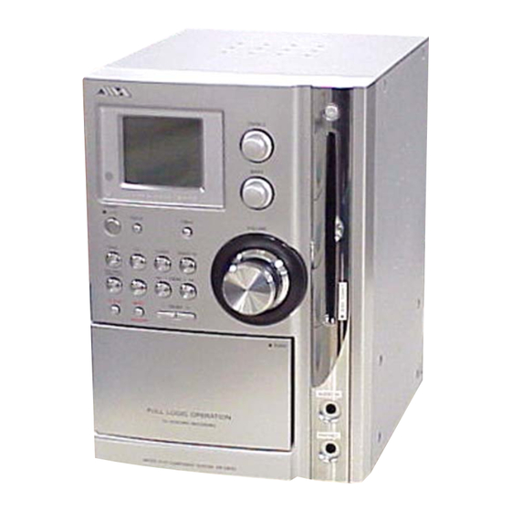
MICRO HI-FI COMPONENT SYSTEM
AEP Model
CX-LDB30/LDB50
UK Model
E Model
CX-LDB30/LDB50
NEW
CDM80BV-F4BD81
BU-F4BD81B
KSM-215CFP/C2NP
CX-LEM330
CMAL5Z220A
Inputs
AUDIO IN (RCA pin jacks):
Sensitivity 700 mV,
impedance 47 kilohms
Outputs
PHONES (stereo mini jack):
accepts headphones with
an impedance of 32 ohms
or more
SPEAKER:
accepts impedance of
6 ohms
CD player section
System
Compact disc and digital
audio system
Laser Diode Properties
Emission duration:
continuous
Laser Output*: Less than
44.6 µW
* This output is the value measurement at a distance of
200 mm from the objective lens surface on the
Optical Pick-up Block with 7 mm aperture
— Continued on next page —
CX-LDB30
Advertisement
Table of Contents

Related Manuals for Sony CX-LDB30


Summary of Contents for Sony CX-LDB30
- Page 1 SERVICE MANUAL AEP Model CX-LDB30/LDB50 UK Model Ver. 1.1 2005.04 CX-LDB30 E Model CX-LDB30/LDB50 CX-LDB30/LDB50 are the Amplifier, CD player, Tape Deck and Tuner section in XR-DB30/DB50. Model Name Using Similar Mechanism CD Mechanism Type CDM80BV-F4BD81 Section Base Unit Name BU-F4BD81B...
- Page 2 COMPONENTS IDENTIFIED BY MARK 0 OR DOTTED LINE WITH MARK 0 ON THE SCHEMATIC DIAGRAMS AND IN THE PARTS LIST ARE CRITICAL TO SAFE OPERATION. REPLACE THESE COMPONENTS WITH SONY PARTS WHOSE PART NUMBERS APPEAR AS SHOWN IN THIS MANUAL OR IN SUPPLEMENTS PUBLISHED BY SONY.
-
Page 3: Table Of Contents
CX-LDB30/LDB50 TABLE OF CONTENTS SERVICING NOTES DIAGRAMS ..........4 7-1. Block Diagram — BD Section — ........25 GENERAL 7-2. Block Diagram — MAIN Section — ......26 ..............5 7-3. Printed Wiring Board — BD Board — ......27 7-4. -
Page 4: Servicing Notes
CX-LDB30/LDB50 SECTION 1 SERVICING NOTES Notes on chip component replacement CAUTION • Never reuse a disconnected chip component. Use of controls or adjustments or performance of procedures • Notice that the minus side of a tantalum capacitor may be other than those specified herein may result in hazardous radiation damaged by heat. -
Page 5: General
CX-LDB30/LDB50 SECTION 2 GENERAL This section is extracted from instruction manual. List of button locations and reference pages How to use this page Illustration number Use this page to find the location of buttons and other DISPLAY ws (15, 21) parts of the system that are mentioned in the text. -
Page 6: Setting The Clock
CX-LDB30/LDB50 Remote control ALPHABETICAL ORDER BUTTON DESCRIPTIONS ?/1 (power) 1 (7, 14, 19) A – O P – Z m/M (rewind/fast forward) CD qh (9, 11, 13, 16, 17) PLAY MODE qk (10, 11, 16, 26, 7 (10, 14, 16) -
Page 7: Disassembly
CX-LDB30/LDB50 SECTION 3 DISASSEMBLY 3-1. DISASSEMBLY FLOW • This set can be disassembled in the order shown below. 3-2.SIDE PANEL (L) (R), TOP PANEL, 3-9.CASSETTE PANEL BACK PANEL (Page 11) (Page 8) 3-3.CD MECHANISM SECTION 3-4.FRONT PANEL SECTION (Page 8) (Page 9) 3-10.CD MECHANISM DECK... -
Page 8: Side Panel (L)(R), Top Panel, Back Panel
CX-LDB30/LDB50 Note: Follow the disassembly procedure in the numerical order given. 3-2. SIDE PANEL (L)(R), TOP PANEL, BACK PANEL 9 screw (QT2+3 × 10) qg connector 2p(CN292) qa top panel q; screw (+BVTP3 × 10) 3 side panel (L) qs two screws (+BVTP3 ×... -
Page 9: Front Panel Section
CX-LDB30/LDB50 3-4. FRONT PANEL SECTION 4 connector 7p (CNA302) 3 w ire (flat type) 7core (CN905) 1 w ire (flat type) 19core (CN904) 9 two claws 2 w ire (flat type) 8core (CN901) 7 screw (QT2+3 × 10) 5 screw (+B3) -
Page 10: Main Board
CX-LDB30/LDB50 3-6. MAIN BOARD 5 tapping screw (B3) 4 w ire (flat type) 0 MAIN board 15core (CN602) 6 two tapping screws (B3) 7 two tapping screws (B3) 9 heat sink (main) 3 screw (+BV3) 8 two tapping screws (B3) -
Page 11: Cassette Deck Mechanism
CX-LDB30/LDB50 3-8. CASSETTE DECK MECHANISM 4 w ire (flat type) 7core 5 cassette deck mechanism 3 two screws (B3) 1 two screws (B3) 2 clamp 3-9. CASSETTE PANEL 2 Open the cassette panel. 1 Push the cassette panel. 3 four claws... -
Page 12: Cd Mechanism Deck (Cdm80Bv-F4Bd81)
CX-LDB30/LDB50 3-10. CD MECHANISM DECK (CDM80BV-F4BD81) 1 four tapping screws (B3) 3 CD HOLDER 2 two claws 4 CD mechanism deck (CDM80BV-F4BD81) 3-11. CHASSIS (TOP) 4 three screws 1 screw (+BVTP 2.6 × 8) (+BVTP 2.6 × 8) 3 two screws (+P 2 ×... -
Page 13: Lever (Loading R/L)
CX-LDB30/LDB50 3-12. LEVER (LOADING R/L) torsion spring (loading LV) torsion spring (loading RV) 5 lever (loading-R) 2 two hooks 4 two hooks 3 lever (loading-L) PRECAUTION DURING LEVER (LOADING R / L) INSTALLATION Align the horizontal position. lever (loading-L) lever (loading-R) Install the both levers so that they move symmetrically. -
Page 14: Disc Stop Lever, Disc Sensor Lever
CX-LDB30/LDB50 3-13. DISC STOP LEVER, DISC SENSOR LEVER 1 gear (cap) 2 gear (IDL-L) PRECAUTION DURING DISC STOP LEVER INSTALLATION chassis (top) hole 5 two hooks 3 two claws disc stop lever 6 disc stop lever hole Install the disc stop lever so that the both holes are aligned. -
Page 15: Bd Board
CX-LDB30/LDB50 3-15. BD BOARD D board 3 Remove the two solderings. 2 Remove the two solderings. 1 CN101 3-16. OPTICAL PICK-UP (KSM-215CFP/C2NP) 4 two floating screws 3 two floating screws (+PTPWHM 2.6) (+PTPWHM 2.6) 5 two insulators 6 two insulators... -
Page 16: Base Unit (Bu-F4Bd81B)
CX-LDB30/LDB50 3-17. BASE UNIT (BU-F4BD81B) 4 floating screw (+PTPWHM 2.6) 6 base unit (BU-F4BD81B) 3 holder down b spring 5 floating screw (+PTPWHM 2.6) 2 lever (CL UP2) 1 screw (+BVTP 2.6 × 8) 3-18. LEVER (BU LOCK) 5 lever (BU lock) -
Page 17: Close Lever
CX-LDB30/LDB50 3-19. CLOSE LEVER 1 washer (3-1-0.4) 5 close lever 3 claw 2 close lever spring 4 shaft disc stop 3-20. DIR LEVER, GEAR (IDL-B) 3 gear pulley capstan retaining ring 4 gear (cap) 5 gear (IDL-A) 8 stopper 9 DIR lever... -
Page 18: Gear (Idl-C)
CX-LDB30/LDB50 3-21. GEAR (IDL-C) 3 gear (IDL-D) 4 three hooks 2 two claws 1 gear (IDL-F) 5 gear loading lever 7 gear (IDL-C) 6 claw... -
Page 19: Test Mode
CX-LDB30/LDB50 SECTION 4 TEST MODE [COLD RESET] [Disc anti-theft] The cold reset clears all data including preset data stored in Procedure: 1. Press the ?/1 button to turn the set on. the RAM to initial conditions. Execute this mode when returning the set to the customer. -
Page 20: Mechanical Adjustments
CX-LDB30/LDB50 SECTION 5 SECTION 6 MECHANICAL ADJUSTMENTS ELECTRICAL ADJUSTMENTS TAPE MECHANISM DECK SECTION DECK SECTION 0 dB=0.775V Precaution 1. Clean the following parts with a denatured alcohol-moistened Precaution swab: 1. Demagnetize the record/playback head with a head record/playback heads pinch rollers demagnetizer. - Page 21 CX-LDB30/LDB50 Record Bias Adjustment 3. Mode: Playback MAIN board Procedure: SPEAKER terminal (J201) test tape L-CH P-4-A100 1. Record mode oscilloscope (10 kHz, –10 dB) MAIN board L-CH AUX IN (J291) 1) 315 Hz 50 mV (–23.8 dB) 2) 10 kHz ...
- Page 22 CX-LDB30/LDB50 RFDC signal waveform CD SECTION VOLT/DIV: 200 mV TIME/DIV: 500 ns Note: 1. Use YEDS-18 disc (3-702-101-01) unless otherwise indicated. 2. Use an oscilloscope with more than 10MΩ impedance. 3. Clean the object lens by an applicator with neutral detergent level: 0.6 ±...
- Page 23 CX-LDB30/LDB50 E-F Balance Adjustment Checking Location: Connection: – BD BOARD (Conductor Side) – oscilloscope BD board TP (TEO) TP (VC) – IC303 Procedure: 1. Connect an oscilloscpe to test point TP (TEO) and TP (VC) on the BD board. 2. AC is put in pushing CD u button to enter the CD test mode.
-
Page 24: Diagrams
CX-LDB30/LDB50 SECTION 7 DIAGRAMS • Circuit Boards Location MAIN board BD board CD EJECT board DRIVER board PANEL board PT board JACK board THIS NOTE IS COMMON FOR PRINTED WIRING BOARDS AND SCHEMATIC DIAGRAMS. (In addition to this, the necessary note is printed in each block.) For Schematic Diagrams. -
Page 25: Block Diagram - Bd Section
CX-LDB30/LDB50 7-1. BLOCK DIAGRAM — BD SECTION — FILTER XTSL CD DSP XTAO IC101 (1/2) CLOCK X171 51 53 50 52 DETECTOR D +3.3V XTAI GENERATOR 16.9344MHz XTACN RFACO RFACI AOUT1 RFAC ASYMMETRY MAIN SUMMING DIGITAL PLL DEMODULATOR CORRECTOR SECTION... -
Page 26: Block Diagram - Main Section
CX-LDB30/LDB50 7-2. BLOCK DIAGRAM — MAIN SECTION — J291 POWER AMP AUDIO IN IC401 FUNCTION IC601 R-CH R-CH J292 AUX-L OUT-L 11 IN-CH1 OUT-CH1 PHONES TUNER-L OUT-R R-CH Q403 OVERLOAD PBP-L CD L RY201 TUNER PACK RECOUT-L R-CH +Vcc PBOR... -
Page 27: Printed Wiring Board - Bd Board
CX-LDB30/LDB50 • See page 24 for Circuit Boards Location. 7-3. PRINTED WIRING BOARD — BD BOARD — :Uses unleaded solder. BD BOARD (COMPONENT SIDE) M101 (SPINDLE) BD BOARD (CONDUCTOR SIDE) C302 IC303 S101 (LIMIT) C305 C303 C255 C260 R404 R313... -
Page 28: Schematic Diagram - Bd Board
CX-LDB30/LDB50 • See page 42, 43 for IC Block Diagrams. • See page 42 for Waveforms. 7-4. SCHEMATIC DIAGRAM — BD BOARD — C131 100p TP423 IOP1 C142 1500p C134 C125 R131 R121 R143 C151 TP10 R203 C143 3.3k TP424... -
Page 29: Printed Wiring Board - Driver Board, Jack Board
CX-LDB30/LDB50 • See page 24 for Circuit Boards Location. 7-5. PRINTED WIRING BOARD — DRIVER BOARD, JACK BOARD — :Uses unleaded solder. DRIVER BOARD JACK BOARD AUDIO IN J291 (CHUKING) C294 C293 R286 C291 C292 R285 C295 R289 CN203 W291... -
Page 30: Schematic Diagram - Driver Board, Jack Board
CX-LDB30/LDB50 • See page 44 for IC Block Diagram. 7-6. SCHEMATIC DIAGRAM — DRIVER BOARD, JACK BOARD — DRIVER BOARD JACK BOARD IC B/D J291 S703 S701 S702 (TRIGGER) (DISC IN/OUT) (CHUKING) AUDIO IN C293 R285 1 50V 2.2k IC701... -
Page 31: Printed Wiring Board - Main Section (1/2)
CX-LDB30/LDB50 • See page 24 for Circuit Boards Location. 7-7. PRINTED WIRING BOARD — MAIN SECTION (1/2) — :Uses unleaded solder. MAIN BOARD (SIDE A) • Semiconductor TAPE MECHANISM DECK HEAD Not used Location ERASE –REC/PB– L CH R CH Ref. -
Page 32: Printed Wiring Board - Main Section (2/2)
CX-LDB30/LDB50 • See page 24 for Circuit Boards Location. 7-8. PRINTED WIRING BOARD — MAIN SECTION (2/2) — :Uses unleaded solder. • Semiconductor Location Ref. No. Location MAIN BOARD (SIDE B) D105 D107 D108 D110 D111 D112 D113 RU, E51... -
Page 33: Schematic Diagram - Main Section (1/5)
CX-LDB30/LDB50 • See page 44 for IC Block Diagram. 7-9. SCHEMATIC DIAGRAM — MAIN SECTION (1/5) — CN602 11P: RU, E51 15P: RDS-DATA RDS DATA RDS-CLK RDS INT C882 R884 NO USE 0.22 2.2k MAIN BOARD (1/5) +3V(RDS) TU-R C867 0.01... -
Page 34: Schematic Diagram - Main Section (2/5)
CX-LDB30/LDB50 7-10. SCHEMATIC DIAGRAM — MAIN SECTION (2/5) — MAIN BOARD (2/5) CD-P-GND CD-D-GND MP3GND CD-A-GND FUNC-GND CD VM(7V) MP3VD MP3(3.3V) D-VDD DVDD(3.3V) A-VDD AVDD(3.3V) IC401 MAIN BOARD MGND (5/5) POWER AMP MGND (Page 37) D-GND MP3GND CD-L CD-L CD-AGND... -
Page 35: Schematic Diagram - Main Section (3/5)
CX-LDB30/LDB50 7-11. SCHEMATIC DIAGRAM — MAIN SECTION (3/5) — MAIN BOARD (1/5) MAIN BOARD (3/5) (Page 33) 9 101112 141516 D602 PB L UDZSTE-174.7B C604 C303 0.001 JR301 C602 C304 Q313 0.001 RT1P141C-TP-1 PB R SWITCH MAIN BOARD (2/5) D304... -
Page 36: Schematic Diagram - Main Section (4/5)
CX-LDB30/LDB50 7-12. SCHEMATIC DIAGRAM — MAIN SECTION (4/5) — MAIN BOARD (2/5) (Page 34) 3233 343536 3738394041 4243 4445 MAIN BOARD (4/5) J201 TERMINAL, 4P SP L-SPG C231 SPEAKER 0.01 R203 D209 1SS355TE-17 Q203 2SC3052F-T1-LF R220 2.2k D205 R-SPG MC2838-T112-1 R217 42.5... -
Page 37: Schematic Diagram - Main Section (5/5)
CX-LDB30/LDB50 7-13. SCHEMATIC DIAGRAM — MAIN SECTION (5/5) — • See page 42 for Waveforms. • See page 45 for IC Pin Function Description. MAIN BOARD (5/5) MGND MGND MGND MGND CNA702 FR-VDD FR-VDD FR-VDD FR-VDD R910 VDD1 VDD1 SW2(CHUCK SW) -
Page 38: Printed Wiring Board - Panel Board
CX-LDB30/LDB50 • See page 24 for Circuit Boards Location. 7-14. PRINTED WIRING BOARD — PANEL BOARD — :Uses unleaded solder. PANEL BOARD R513 CD EJECT BOARD R508 C503 R512 C506 L C D 5 0 1 D501 C908 TREBLE J W 5 0 6... -
Page 39: Schematic Diagram - Panel Board
CX-LDB30/LDB50 7-15. SCHEMATIC DIAGRAM — PANEL BOARD — DISP_GND PANEL BOARD D501 R505 UDZSTE-175.1B C908 1 10V CD EJECT BOARD R508 FR-VDD CN502 W550 S550 CD EJECT +VM(7V) +VM(7V) KEY_GND DISP_GND FR-VDD FR-VDD(3.3V) LCSB LED_BKLIGHT LCD501 LCD-RS KEY_GND LCD BACK LIGHT... -
Page 40: Printed Wiring Board - Pt Board
CX-LDB30/LDB50 • See page 24 for Circuit Boards Location. 7-16. PRINTED WIRING BOARD — PT BOARD — :Uses unleaded solder. PT BOARD JW013 JW018 JW014 JW016 AEP, RU JW006 PT 003 AEP, RU JW017 D002 AC IN P T0 JW004... -
Page 41: Schematic Diagram - Pt Board
CX-LDB30/LDB50 7-17. SCHEMATIC DIAGRAM — PT BOARD — PT BOARD PT001 MAIN PT 80W 230V JW009 CN001 NEUTRAL NEUTRAL W001 LIVE LIVE JW005 JW008 JW001 JW004 JW002 JW011 CN002 RY001 VH(AC) G5PA-1 RY002 VOLT SELECTOR VL(AC) GND(M) VL(AC) VH(AC) MAIN BOARD... - Page 42 CX-LDB30/LDB50 • Waveforms – BD Board – – MAIN Board – IC101 CXD3059AR IC101 ra (RFACO) IC901 qg (16MHz-IN) 115 114 112 111 110 109 103 102 101 100 119 118 1.2 Vp-p 1.4 Vp-p 62.7 ns (16 MHz) CPU INTERFACE 200 mV/DIV, 1 µ...
- Page 43 CX-LDB30/LDB50 IC301 TC94A34FG-002 Timing Generator VDDP PO5/AD5 /RESET PO6/AD6 STANDBY PO7AD7 /MICS /MILP MIDIO AD10 VDDT /MICK /MIACK/ SRMSTB AD16 VDDT VDDM PO8/AD11 SDO0 PO9/AD12 /CCE/ PO10/ BCKO AD13 BUCK/ PO11/ LRCKO AD14 SDO3/ SDI0 Interrupt Timer Control Switch General...
- Page 44 CX-LDB30/LDB50 — MAIN Board — IC601 BD3882FV BASS MIDDLE BASS REAR VOLUME REAR VOLUME FRONT TREBLE VOLUME LOGIC CONTROL FRONT TREBLE MIDDLE VOLUME — DRIVER Board — IC701 BA6956AN CONTROL LOGIC...
- Page 45 CX-LDB30/LDB50 • IC Pin Function Description MAIN BOARD IC901 M30622MEP-A26FPU0 (SYSTEM CONTROLLER) Pin No. Pin Name Description O-LCDATA LCD DATA O-LCDSCK Data output to the fluorescent indicator tube O-VOLUMELED LED (i-Bass/DEMO) control signal output I-RMC Remote control signal input from the remote sensor...
- Page 46 CX-LDB30/LDB50 Pin No. Pin Name Description O-FUNCCLK Clock output to the function IC (IC601) I-PLAY SW PLAY switch signal input from the tape deck O-LCDCS Chip select signal output to the fluorescent indicator tube O-SOL Solenoid control signal output to the tape deck...
-
Page 47: Exploded Views
CX-LDB30/LDB50 Ver. 1.1 SECTION 8 EXPLODED VIEWS NOTE: • -XX and -X mean standardized parts, so they • The mechanical parts with no reference The components identified by mark 0 or may have some difference from the original number in the exploded views are not supplied. -
Page 48: Front Panel Section
CX-LDB30/LDB50 Ver. 1.1 8-2. FRONT PANEL SECTION supplied 72 73 supplied 61 63 supplied Ref. No. Part No. Description Remark Ref. No. Part No. Description Remark 2-514-936-01 PANEL, CASSETTE (LDB50) X-2025-175-1 KEY ASSY, FUNC (A) 2-514-936-11 PANEL, CASSETTE (LDB30) X-2025-176-1 KEY ASSY, FUNC (B) -
Page 49: Chassis Section
CX-LDB30/LDB50 Ver. 1.1 8-3. CHASSIS SECTION supplied supplied PT001 supplied supplied supplied Ref. No. Part No. Description Remark Ref. No. Part No. Description Remark A-1091-001-A MAIN BOARD, COMPLETE (LDB50: AEP) 1-828-987-11 WIRE (FLAT TYPE) (15 CORE) (AEP, UK) A-1091-956-A MAIN BOARD, COMPLETE (LDB30: AEP, UK) -
Page 50: Cd Mechanism Deck Section 1 (Cdm80Bv-F4Bd81)
CX-LDB30/LDB50 8-4. CD MECHANISM DECK SECTION 1 (CDM80BV-F4BD81) M701 Ref. No. Part No. Description Remark Ref. No. Part No. Description Remark 4-985-672-01 SCREW (+PTPWHM2.6), FLOATING 4-245-630-01 LEVER (SW) 2-515-538-01 SPRING (HOLDER DOWN B), COIL 4-951-620-01 SCREW (2.6X8), +BVTP 4-245-653-01 BELT (MOT) -
Page 51: Cd Mechanism Deck Section 2 (Cdm80Bv-F4Bd81)
CX-LDB30/LDB50 8-5. CD MECHANISM DECK SECTION 2 (CDM80BV-F4BD81) supplied Ref. No. Part No. Description Remark Ref. No. Part No. Description Remark 4-245-627-01 WASHER (6-2.7-0.4) 4-245-640-01 GEAR (CAP) 4-245-637-01 ROLLER, RUBBER 4-251-780-01 CAP (CLAMP 215V) 4-245-649-01 GEAR (IDL-I) 4-245-638-01 LEVER (CL UP1) 4-245-657-01 LEVER (LOADING-R) 4-985-672-01 SCREW (+PTPWHM2.6), FLOATING... -
Page 52: Cd Mechanism Deck Section 3 (Cdm80Bv-F4Bd81)
CX-LDB30/LDB50 8-6. CD MECHANISM DECK SECTION 3 (CDM80BV-F4BD81) supplied supplied Ref. No. Part No. Description Remark Ref. No. Part No. Description Remark 4-245-643-01 GEAR (IDL-C) 4-245-640-01 GEAR (CAP) 4-245-644-01 GEAR (IDL-D) 4-245-628-01 LEVER (BU LOCK) 2-515-536-01 SPRING (DIR), TENSION COIL 4-245-642-01 GEAR (IDL-B) 4-248-206-01 WASHER (3-1-0.4) -
Page 53: Base Unit Section
CX-LDB30/LDB50 8-7. BASE UNIT SECTION S101 Ref. No. Part No. Description Remark Ref. No. Part No. Description Remark 0 301 8-820-252-01 OPTICAL PICK-UP (KSM-215CFP) 4-216-085-01 SPRING (F-1), TENSION (including M101,M102) 4-216-086-01 SPRING (F-2), TENSION A-4751-434-A BD BOARD, COMPLETE 1-827-992-11 WIRE (FLAT TYPE) (16 CORE) 4-985-672-01 SCREW (+PTPWHM2.6), FLOATING... -
Page 54: Electrical Parts List
CX-LDB30/LDB50 SECTION 9 ELECTRICAL PARTS LIST NOTE: • Due to standardization, replacements in the • COILS • SEMICONDUCTORS uH: µH In each case, u: µ, for example: parts list may be different from the parts uA. . : µA. . , uPA. . , µPA. . , specified in the diagrams or the components •... - Page 55 CX-LDB30/LDB50 CD EJECT DRIVER JACK Ref. No. Part No. Description Remark Ref. No. Part No. Description Remark < TRANSISTOR > R410 1-216-809-11 METAL CHIP 1/10W R411 1-216-809-11 METAL CHIP 1/10W 6-551-120-01 TRANSISTOR 2SA2119K R412 1-216-809-11 METAL CHIP 1/10W < RESISTOR >...
- Page 56 CX-LDB30/LDB50 Ver. 1.1 JACK MAIN Ref. No. Part No. Description Remark Ref. No. Part No. Description Remark < JACK > C130 1-126-947-11 ELECT 47uF C131 1-107-826-11 CERAMIC CHIP 0.1uF J291 1-815-629-11 JACK (AUDIO IN) C132 1-107-826-11 CERAMIC CHIP 0.1uF J292...
- Page 57 CX-LDB30/LDB50 Ver. 1.1 MAIN Ref. No. Part No. Description Remark Ref. No. Part No. Description Remark C422 1-164-156-11 CERAMIC CHIP 0.1uF C670 1-165-176-11 CERAMIC CHIP 0.047uF C423 1-164-156-11 CERAMIC CHIP 0.1uF C671 1-165-176-11 CERAMIC CHIP 0.047uF C424 1-126-968-11 ELECT 100uF...
- Page 58 CX-LDB30/LDB50 MAIN Ref. No. Part No. Description Remark Ref. No. Part No. Description Remark CN904 1-779-287-11 CONNECTOR, FFC (LIF (NON-ZIF)) 19P < IC > CN905 1-568-826-11 CONNECTOR, FFC 7P IC101 8-759-231-58 IC TA7812S < DIODE > IC102 8-759-071-48 IC TA7807S...
- Page 59 CX-LDB30/LDB50 MAIN Ref. No. Part No. Description Remark Ref. No. Part No. Description Remark Q205 8-729-600-22 TRANSISTOR 2SA1235TP-1EF R133 1-216-841-11 METAL CHIP 1/10W Q206 8-729-120-28 TRANSISTOR 2SC3052F-T1-LF R134 1-216-841-11 METAL CHIP 1/10W R135 1-216-821-11 METAL CHIP 1/10W Q207 8-729-120-28 TRANSISTOR...
- Page 60 CX-LDB30/LDB50 MAIN Ref. No. Part No. Description Remark Ref. No. Part No. Description Remark R230 1-216-825-11 METAL CHIP 2.2K 1/10W R422 1-216-837-11 METAL CHIP 1/10W R231 1-216-829-11 METAL CHIP 4.7K 1/10W R423 1-216-833-11 METAL CHIP 1/10W R232 1-216-829-11 METAL CHIP 4.7K...
- Page 61 CX-LDB30/LDB50 MAIN Ref. No. Part No. Description Remark Ref. No. Part No. Description Remark R610 1-216-797-11 METAL CHIP 1/10W R675 1-216-809-11 METAL CHIP 1/10W R676 1-216-809-11 METAL CHIP 1/10W R611 1-216-813-11 METAL CHIP 1/10W R677 1-216-845-11 METAL CHIP 100K 1/10W...
-
Page 62: Main Panel
CX-LDB30/LDB50 Ver. 1.1 MAIN PANEL Ref. No. Part No. Description Remark Ref. No. Part No. Description Remark R787 1-216-829-11 METAL CHIP 4.7K 1/10W R994 1-216-813-11 METAL CHIP 1/10W R788 1-216-829-11 METAL CHIP 4.7K 1/10W (RU) R789 1-216-809-11 METAL CHIP 1/10W... - Page 63 CX-LDB30/LDB50 Ver. 1.1 PANEL Ref. No. Part No. Description Remark Ref. No. Part No. Description Remark < TRANSISTOR > < SWITCH > Q502 8-729-027-46 TRANSISTOR RT1N144C-TP-1 (LDB50) S501 1-477-823-11 ENCODER, ROTARY (VOLUME) Q503 8-729-120-28 TRANSISTOR 2SC3052F-T1-LF S502 1-418-859-21 ENCODER, ROTARY (BASS)
- Page 64 CX-LDB30/LDB50 Ver. 1.1 Ref. No. Part No. Description Remark R008 1-216-797-11 METAL CHIP 1/10W (AEP, UK, RU) R008 1-216-864-11 SHORT CHIP 0 (E51) < RELAY > 0 RY001 1-755-334-11 RELAY, AC POWER (AEP, RU) 0 RY002 1-755-496-11 RELAY (E51) < SWITCH >...
- Page 65 CX-LDB30/LDB50 MEMO...
-
Page 66: Revision History
Clicking the version allows you to jump to the revised page. Also, clicking the version at the upper right on the revised page allows you to jump to the next revised page. Ver. Date Description of Revision 2005.02 2005.04 Addition of UK model for CX-LDB30...
Need help?
Do you have a question about the CX-LDB30 and is the answer not in the manual?
Questions and answers