
Related Manuals for LG TCH-M550


Summary of Contents for LG TCH-M550
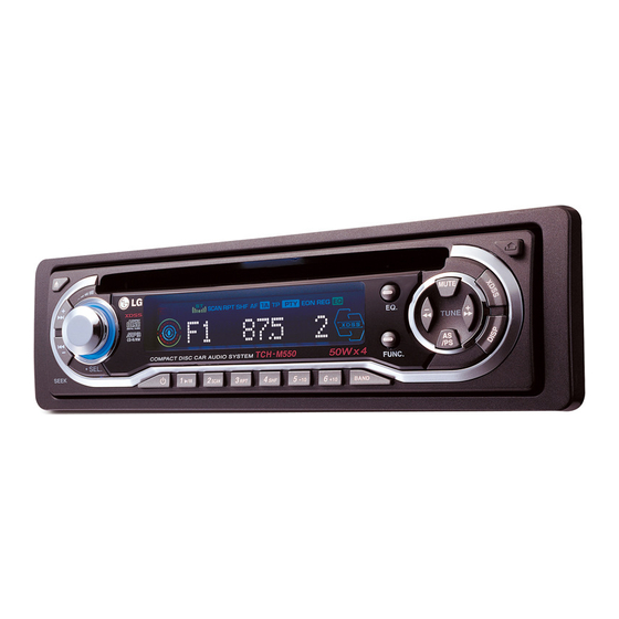
- Page 1 DETACHABLE FRONT PANEL CAR CD RECEIVER SERVICE MANUAL CAUTION BEFORE SERVICING THE UNIT, READ THE “SAFETY PRECAUTIONS” IN THIS MANUAL. MODEL : TCH-M550...
-
Page 2: Table Of Contents
[CONTENTS] SECTION 1. SUMMARY • SERVICING PRECAUTIONS ......................1-2 • ESD PRECAUTIONS ........................1-3 • SPECIFICATIONS ........................... 1-4 SECTION 2. ELECTRICAL • ELECTRICAL TROUBLESHOOTING GUIDE ................. 2-1 • CD PART TROUBLESHOOTING GUIDE ..................2-3 • WAVEFORMS OF MAJOR CHECK POINT .................. 2-11 •... -
Page 3: Section 1. Summary
SECTION 1. SUMMARY SERVICING PRECAUTIONS Always disconnect the power source before: 1) Removing or reinstalling any component, circuit board, module or any other instrument assembly. 2) Disconnecting or reconnecting any instrument electrical plug or other electrical connection. 3) Connecting a test substitute in parallel with an electrolytic capacitor in the instrument. CAUTION: A wrong part substitution or incorrect polarity installation of electrolytic capacitors may result in an explosion hazard. -
Page 4: Esd Precautions
ESD PRECAUTIONS [Electrostatically Sensitive Devices (ESD)] Some semiconductor (solid state) devices can be damaged easily by static electricity. Such omponents commonly are called Electrostatically Sensitive Devices (ESD). Examples of typical ESD devices are integrated circuits and some field-effect transistors and semiconductor chip components. The following techniques should be used to help reduce the incidence of component damage caused by static electricity. -
Page 5: Specifications
SPECIFICATIONS 1. GENERAL Power requirements ........................DC12V~15V Ground system ........................... Negative Dimensions(W x H x D) ...................... 188 x 58 x 166mm Weight .............................. Net: 1.3kg 2. RADIO SECTION AM(MW) Frequency range 65.0~74.0MHz(Optional), 522~1,620kHz 87.5~108MHz (Optional:530~1,710kHz/ 520~1,620kHz) Intermediate frequency 10.8MHz 450kHz Usable sensitivity 12dBµV... -
Page 6: Section 2. Electrical
SECTION 2. ELECTRICAL ELECTRICAL TROUBLESHOOTING GUIDE (1) No Power. Any Key power on. Check power supply circuitry. Q260, Q380, Q381, IC401 Is power turnd on? IC201 Pin2 Check loading supply circuitry. DISC loading? Q350,Q351,PN505, IC401 Pin1 Check laser circuitry. Does initial reading occur? Q501, IC502 Check focusing circuitry. - Page 7 (2) LCD light abnornal. Any Key power on. (without DISC) Power supply circuitry Check voltage in the power defective. Do display LCD then light? supply circuitry. Q380,Q381,IC403 Is u-com IC401 reset circuit Reset circuit defective. normal? Pin10 IC201 Surrounding circuit defective.
- Page 8 - 2-3 -...
- Page 9 - 2-4 -...
- Page 10 - 2-5 -...
- Page 11 - 2-6 -...
- Page 12 - 2-7 -...
- Page 13 - 2-8 -...
- Page 14 - 2-9 -...
- Page 15 - 2-10 -...
-
Page 16: Waveforms Of Major Check Point
WAVEFORMS OF MAJOR CHECK POINT #1. MICOM INTERFACE WAVEFORM #2. SLED DRIVE AND MOTOR WAVEFORM (CN503 1 9,2 1 ,1 8,20) during normal play (IC504 pin5, 1 4) when focus search #3. FOCUS DRIVE AND MOTOR WAVEFORM (R5 1 3, IC504 pin 1 5) •... - Page 17 #4. SPINDLE DRIVE AND MOTOR WAVEFORM #5. TRACK DRIVE AND MOTOR WAVEFORM (IC504 pin6, 1 2) when TOC reading (R508, IC504 pin23) during normal play #6. RF, TRACKING AND FOCUS ERROR WAVEFORM (IC502 pin8, 2 1 , 23) during normal play - 2-12 -...
-
Page 18: Internal Block Diagram Of Ics
INTERNAL BLOCK DIAGRAM of ICs IC401 uPD784214A 1) PORT ASSIGNMENT PCD_PWR (O) PRDS_DI (I) PTUN_PWR (O) PST (I) PPWR (O) N.C. PTEL_MUTE (I) N.C. PREMOTE (O) N.C. PLIGHT (O) PDSP_OCLK (O) N.C. PDSP_ODA (O) PSTANDBY (O) PDSP_IDA (O) PBEEP (O) PEV_CLK (O) PPLL_CE (O) PEV_DO (O) - Page 19 2) PORT DESCRIPTION Name in Micom Name in Model Enable I/O I/O setted Output Format Descripation P60/A16 PCD_PWR CMOS DSP power suppler ON output P61/A17 PTUN_PWR CMOS Tuner power supplier ON output P62/A18 PPWR CMOS System power supplier ON output P63/A19 PTEL_MUTE Telephone mute input...
- Page 20 AVSS AVSS Ground for A/D converter and D/A converter P130/ANO0 N.C. CMOS Not to be used (Open) P131/ANO1 N.C. CMOS Not to be used (Open) AVREF1 AVREF1 Reference voltage applied to A/D converter P70/RxD2/SI2 N.C. CMOS Not to be used (Open) P71/RxD2/SO2 PFRT_DO CMOS...
- Page 21 IC501 MN6627933 1) PORT ASSIGNMENT - 2-16 -...
- Page 22 2) Block Diagram - 2-17 -...
- Page 23 3) PORT DESCRIPTION Pin No. Symbol Function DRAM data signal I/O 11 DRAM data signal I/O 10 DRAM data signal I/O 9 DRAM data signal I/O 8 UDQM SDRAM upper byte data mask signal output SDRCK SDRAM clock signal output DRAM address signal output 11 DRAM address signal output 9 DRAM address signal output 8...
- Page 24 Pin No. Symbol Function LOOUTR R-ch audio output for line-out output LOVDD1 Power supply for line-out output N.C. TMON1 Test monitor output 1 N.C. N.C. TMON2 Test monitor output 2 DVDD3 Power supply 3 for digital circuits DVSS2 Ground 2 for digital circuits *EXT0 Expansion I/O port 0 *EXT1...
-
Page 25: Block Diagram
IC503 M12L16161A 1) PORT ASSIGNMENT 2) BLOCK DIAGRAM Data Input Regidter Bank Select LDQM 512K x 16 512K x 16 Column Decoder Latency & Burst Length LCKE Programming Register LRAS LDQM LCBR LCAS LWCBR Timing Register L(U)DQM - 2-20 -... - Page 26 PIN Function table Name Input Function System Clock Active on the positive going edge to sample all inputs. Disables or enables device operation by masking or enabling all inputs except Chip Select CLK, CKE and L(U)DQM. Masks system clock to freeze operation from the next clock cycle. CKE Clock Enable should be enabled at least one cycle prior to new command.
- Page 27 IC505 AMC1117 BLOCK DIAGRAM - 2-22 -...
- Page 28 IC601 PT2313L LOUT LOUD_L BOUT_L BIN_L TREB_L Speaker LFOUT LIN1 LIN1 Mute LIN2 LIN2 Speaker LIN3 Voume & Bass Treble LIN3 Loudness Input LROUT Selector Mute RIN3 & Gain RIN3 Serial Bus Decoder & Latches RIN2 Control RIN2 DATA RIN1 RIN1 DGND Speaker...
- Page 29 IC801 TA8275H IC901 LC75811 - 2-24 -...
- Page 30 ❏ BLOCK DIAGRAM L-SPEAKER POWER AMP 2(FL,FR) TA8275H 11,14 24,25 FRONT R-SPEAKER 21,23 LINE SW/E.VOLUME 10,14 22,23 12,15 2(RL,FR) L-SPEAKER 17,19 13,19 10,14 REAR TU101 3, 5 R-SPEAKER 11,12 2, 8, 18, 24 OP AMP 9.4V REG CET85XX 2(LR) S4560 Q360,ZD361 MUTE 16,17,...
-
Page 31: Main Schematic Diagram
❏ SCHEMATIC DIAGRAM • MAIN SCHEMATIC DIAGRAM 2-27 2-28... -
Page 32: Front Schematic Diagram
• FRONT SCHEMATIC DIAGRAM 2-29 2-30... -
Page 33: Cdp Schematic Diagram
• CDP SCHEMATIC DIAGRAM 2-31 2-32... -
Page 34: Printed Circuit Diagram
❏ PRINTED CIRCUIT DIAGRAM • LED P.C.BOARD • FRONT P.C. BOARD (SOLDER SIDE) • LED P.C.BOARD • FRONT P.C. BOARD (COMPONENT SIDE) 2-33 2-34... - Page 35 • MAIN P.C. BOARD 2-35 2-36...
- Page 36 • CDP P.C. BOARD • CDP P.C. BOARD 2-37 2-38...
-
Page 37: Section 3. Cabinet Mainchassis & Mechanism
SECTION 3. CABINET MAINCHASSIS & MECHANISM I EXPLODED VIEW CAUTION NOTE) Refer to “SECTION 4 REPLACEMENT PARTS LIST” in order to look for the Exposed blade will cause part number of each part. severe injury...
Need help?
Do you have a question about the TCH-M550 and is the answer not in the manual?
Questions and answers