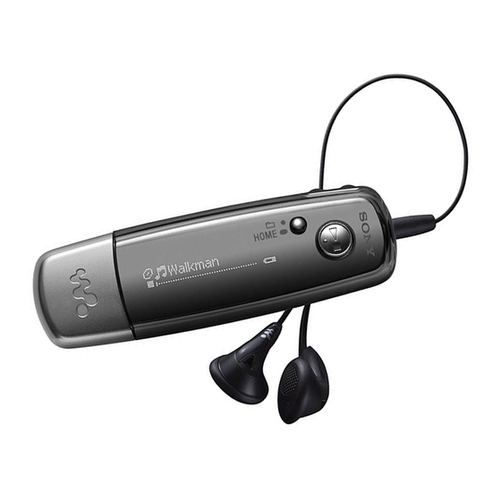
Sony NW-E002F Service Manual
Sony digital music player service manual
Hide thumbs
Also See for NW-E002F:
- Operation manual (80 pages) ,
- Quick start manual (12 pages) ,
- Guía de funcionamiento manual (78 pages)
Table of Contents
Advertisement
NW-E002F/E003F/E005F
SERVICE MANUAL
Ver. 1.5 2006.11
US and foreign patents licensed from
Dolby Laboratories.
Supported bit rates
MP3: 32 to 320 kbps variable bit rate-compliant
WMA: 32 to 192 kbps variable bit rate-compliant
ATRAC: 48/64/66 (ATRAC3)*/96/105 (ATRAC3)*/
128/132 (ATRAC3)/160/192/256/320/352 kbps
* CD recording cannot be done using SonicStage software
in ATRAC3 at 66/105 kbps.
Sampling frequency*
MP3: 32, 44.1, 48 kHz
WMA: 44.1 kHz
ATRAC: 44.1 kHz
* Sampling frequency may not correspond to all encoders.
Frequency response
20 to 20,000 Hz (single signal measurement)
FM Frequency range
87.5 to 108.0 MHz
IF (FM)
375 kHz
Antenna
Headphone cord antenna
Interface
Headphone: Stereo mini
Hi-speed USB (USB 2.0 compliant)
Operating temperature
5°C to 35°C (67°F to 95°F)
Power source
• Built-in rechargeable lithium-ion battery
• USB power (from a computer through the USB
connector of the player)
Sony Corporation
9-887-213-06
Connect Business Division
2006K16-1
Published by Sony Techno Create Corporation
© 2006.11
SPECIFICATIONS
Battery life (continuous playback)*
ATRAC format: Approximately 28 hours (Playback at 132 kbps)
ATRAC format: Approximately 25 hours (Playback at 128 kbps)
ATRAC format: Approximately 27 hours (Playback at 48 kbps)
MP3 format: Approximately 27 hours (Playback at 128 kbps)
WMA format: Approximately 19 hours (Playback at 128 kbps)
FM radio reception: Approximately 8 hours
Dimension (w/h/d)
24.8 × 79.0 × 13.6 mm (1 × 3 1/8 × 9/16 inches)
(w/h/d, projecting parts not included)
Mass
Approx. 25 g (0.9 oz)
Audio compression technology
– MPEG-1 Audio Layer-3 (MP3)
– Windows Media Audio (WMA)
– Adaptive Transform Acoustic Coding (ATRAC)
Maximum recordable number of songs and time (Approx.)*
* When transferring four-minute songs.
NW-E002F
Bit rate
Songs
Time
48 kbps
340
22 hr. 40 min.
64 kbps
255
17 hr. 00 min.
96 kbps
170
11 hr. 20 min.
128 kbps
125
8 hr. 20 min.
132 kbps
120
8 hr. 00 min.
160 kbps
100
6 hr. 40 min.
192 kbps
85
5 hr. 40 min.
256 kbps
64
4 hr. 10 min.
320 kbps
51
3 hr. 20 min.
352 kbps
46
3 hr. 00 min.
Canadian Model
HOME
Chinese Model
Bit rate
48 kbps
64 kbps
96 kbps
128 kbps
132 kbps
160 kbps
192 kbps
256 kbps
320 kbps
352 kbps
Capacity
(User available capacity)*
512 MB (Approx. 482 MB = 505,724,928 bytes)
1 GB (Approx. 968 MB = 1,015,726,080 bytes)
2 GB (Approx. 1.89 GB = 2,035,974,144 bytes)
* Available storage capacity of the player may vary.
A portion of the memory is used for data management
NW-E003F
functions.
Songs
Time
Supplied accessories
685
45 hr. 00 min.
Headphones (1)
515
34 hr. 20 min.
CD-ROM* (1)
- SonicStage software
345
23 hr. 00 min.
- Operation Guide (PDF file)
260
17 hr. 20 min.
Quick Start Guide (1)
250
16 hr. 40 min.
* Do not attempt to play this CD-ROM in an audio CD
205
13 hr. 40 min.
player.
170
11 hr. 20 min.
Design and specifications are subject to change without
130
8 hr. 40 min.
notice.
100
6 hr. 40 min.
94
6 hr. 10 min.
DIGITAL MUSIC PLAYER
US Model
NW-E002F/E003F/E005F
AEP Model
NW-E002F/E003F
E Model
Tourist Model
NW-E002F/E003F/E005F
NW-E005F
Songs
Time
1,350
90 hr. 00 min.
1,000
66 hr. 40 min.
690
46 hr. 00 min.
520
34 hr. 40 min.
500
33 hr. 20 min.
415
27 hr. 40 min.
345
23 hr. 00 min.
260
17 hr. 20 min.
205
13 hr. 40 min.
185
12 hr. 20 min.
Advertisement
Table of Contents


Need help?
Do you have a question about the NW-E002F and is the answer not in the manual?
Questions and answers