Table of Contents
Advertisement
Quick Links
COLOR MONITOR
SERVICE MANUAL
CHASSIS NO. : CA-90
FACTORY MODEL: CB777F
MODEL: StudioWorks 700S
StudioWorks 700B
*(
) ID LABEL Model No.
CAUTION
BEFORE SERVICING THE UNIT,
READ THE SAFETY PRECAUTIONS IN THIS MANUAL.
MENU
SELECT
Website:http://biz.LGservice.com
E-mail:http://www.LGEservice.com/techsup.html
(CB777F-NA),
StudioWorks 700E
(CB777F-EA), LN777F(LN777F)
(CB777F-AA)
Advertisement
Table of Contents

Related Manuals for LG CB777F-AA


Summary of Contents for LG CB777F-AA
-
Page 1: Color Monitor
COLOR MONITOR SERVICE MANUAL CHASSIS NO. : CA-90 FACTORY MODEL: CB777F MODEL: StudioWorks 700S (CB777F-NA), StudioWorks 700E (CB777F-AA) StudioWorks 700B (CB777F-EA), LN777F(LN777F) ) ID LABEL Model No. CAUTION BEFORE SERVICING THE UNIT, READ THE SAFETY PRECAUTIONS IN THIS MANUAL. MENU... -
Page 2: Table Of Contents
CONTENTS SPECIFICATIONS ........... 2 DESCRIPTION OF BLOCK DIAGRAM....12 SAFETY PRECAUTIONS ........3 ADJUSTMENT ............14 TIMING CHART ............4 TROUBLESHOOTING GUIDE ......16 OPERATING INSTRUCTIONS ........ 5 EXPLODED VIEW........... 26 CONTROL LOCATIONS ......... 6 REPLACEMENT PARTS LIST ....... 28 WIRING DIAGRAM .......... -
Page 3: Safety Precautions
25.5kV. The following steps describe modify the original design without obtaining written how to measure the high voltage and how to prevent X- permission from LG or you will void the original parts and radiation. labor guarantee. -
Page 4: Timing Chart
TIMING CHART VIDEO SYNC FACTORY PRESET MODE MODE MARK MODE 1 MODE 2 MODE 3 MODE 4 MODE 5 MODE 6 MODE 7 MODE 8 MODE 9 MODE 10 MODE 11 — — — — — Sync Polarity 46.88 53.68 68.677 37.88 60.02... -
Page 5: Operating Instructions
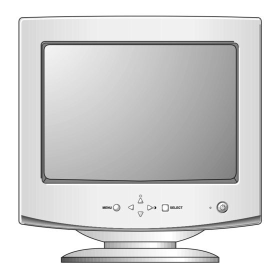
OPERATING INSTRUCTIONS FRONT VIEW REAR VIEW ID Label MENU SELECT Power ON/OFF Button See Front Control Panel AC Power Socket Signal Connector Front Control Panel MENU SELECT Button 1. Power ON/OFF Button Use these buttons to choose or adjust items in the on Use this button to turn the monitor ON or OFF. -
Page 6: Control Locations
CONTROL LOCATIONS CONTROL MAIN Ref. No. Control Function Control Function Ref. No. SW207 POWER BUTTON OSD ADJUSTMENT(RIGHT) SW202 SW204 OSD SELECT MENU BUTTON SW201 SW205 OSD ADJUSTMENT(UP) B+ ADJUSTMENT VR901 SW203 OSD ADJUSTMENT(DAUN) SW206 OSD ADJUSTMENT(LEFT) - 6 -... -
Page 7: Wiring Diagram
WIRING DIAGRAM CABINET P201 P102 P405 P501 P902 P702 TO G2 P402 Socket Signal Cable P302 P301 - 7 -... -
Page 8: Disassembly
DISASSEMBLY 1. TILT/SWIVEL & BACK COVER REMOVAL 1) Set the monitor face downward. 2) Pressing the latch (a), carefully remove the Tilt/Swivel by pulling it upward. 3) Pressing the latch (b), Back cover by pushing it upward. 4) Release the latch (c). 5) Slide the Back Cover away from the Front Cabinet of the monitor. - Page 9 Figure.1 2. TOTAL CHASSIS ASSEMBLY REMOVAL Anode Cap Figure.1) 1) Carefully separate the CDT Board Assembly from the CDT neck. 2) Discharge the remaining static electricity by shorting between the Anode Cap and the CDT ground. 3) Disconnect the Anode Cap from the CDT.
- Page 10 4. CONTROL PCB ASSEMBLY REMOVAL 1) Remove the screw (a). 2) Remove the Control PCB. 5. BOTTOM BRACKET REMOVAL 1) Remove two holer (a). 2) Remove three screw (b). 3) Remove the Bottom Bracket. - 10 -...
-
Page 11: Block Diagram
BLOCK DIAGRAM Dynamic Focus Static Focus Screen - 11 -... -
Page 12: Description Of Block Diagram
DESCRIPTION OF BLOCK DIAGRAM 1. Line Filter & Associated Circuit. 6. Horizontal and Vertical Oscillation. This is used for suppressing noise of power input line This circuit generates the horizontal pulse and the vertical flowing into the monitor and/or some noise generated in pulse by taking the H and V sync signal. - Page 13 15. Video Pre-Amp Circuit. 16. Video Output Amp Circuit. This circuit amplifies the analog video signal from 0-0.7V This circuit amplifies the video signal which comes from to 0-4V. It is operated by taking the clamp, R, G, B drive the video pre-amp circuit and amplified it to applied the and contrast signal from the Micom(IC401).
-
Page 14: Adjustment
ADJUSTMENT GENERAL INFORMATION 7) Adjust tilt as arrow keys to be the best condition. All adjustment are thoroughly checked and corrected 8) DIST. ADJ. → BALANCE command. when the monitor leaves the factory, but sometimes several adjustments may be required. 9) Adjust parallelogram as arrow keys to be the best Adjustment should be following procedure and after condition. - Page 15 17) COLOR ADJ. → LUMINANCE → ABL command. Set G-DRIVE to 90(5A) at DRIVE of the alignment program. 18) Adjust ABL to 34 ± 1FL of the luminance. Adjust R-DRIVE and B-DRIVE command to white 19) Exit from the program. ±...
-
Page 16: Troubleshooting Guide
TROUBLESHOOTING GUIDE 1. NO POWER NO POWER (POWER INDICATOR OFF) CHECK TROUBLE IN FUSE FUSE OK? (F901) CHECK C908 VOLTAGE? TROUBLE IN (AC120V: 160VDC, D900 AC220V: 304VDC) CHECK IC901 PIN 6 TROUBLE IN WAVEFORM (SQUARE WAVE IC901 COMES OUT?) CHECK TROUBLE IN D941, D942, D951, D961, D941, D942, D951, D961,... - Page 17 2. NO CHARACTER NO CHARACTER CHECK TROUBLE IN IC302 P302 5V LINE PIN 9(5V) ? TROUBLE IN CHECK PC SIGNAL, IC302 PIN 5, 6, 7? P301 SIGNAL CABLE CHECK TROUBLE IN IC302 PIN 20, 19, 18 ? IC302 CHECK TROUBLE IN IC303 PIN 4 (80V) P303 15V LINE/ PIN 8 (12V) ?
- Page 18 3. NO RASTER NO VIDEO (POWER INDICATOR ON) CHECK AMBER DPM MODE POWER INDICATOR (NO H and/or V SYNC) GREEN or AMBER? GREEN CHECK TROUBLE IN D712 ANODE D712 (-157V)? CHECK TROUBLE IN G1 VOLTAGE? Q704 (-40V~-60V) CHECK TROUBLE IN CDT HEAT D941, Q942, Q941 VOLTAGE? (6.3V)
- Page 19 4. NO HORIZONTAL DEFLECTION NO H-DEFLECTION (ONE VERTICAL LINE) CHECK TROUBLE IN Q706? Q706 CHECK TROUBLE IN B + VOLTAGE 50V LINE (50V)? CHECK T701(FBT) PIN 2 TROUBLE IN (31KHZ 60V, Q719, Q720, D710 69KHZ 140V) ? CHECK TROUBLE IN Q705 COLLECTOR Q705, T703 WAVEFORM?
- Page 20 5. TROUBLE IN H-LINEARITY UNBALANCED OF H-LIN. CHECK TROUBLE IN IC401 IC401 (MICOM) PIN 22, 23, 24 ? CHECK TROUBLE IN Q711~Q716? Q711 ~ Q716 CHECK TROUBLE IN L703? L703 Cs SIGNAL TABLE HORIZONTAL FREQUENCY(fH) TROUBLE IN 29K ~ 33.9K C722, C723, C726, C729 34K ~ 38.9K 39K ~ 44.9K...
-
Page 21: No Vertical Deflection
6. NO VERTICAL DEFLECTION NO V-DEFLECTION (ONE HORIZONTAL LINE) CHECK TROUBLE IN IC601 PIN 3 R603 15V LINE (15V)? TROUBLE IN CHECK HIGH-VOLTAGE OUT IC601 PIN 7 CIRCUIT(FBT), (40V)? D721, R606 CHECK TROUBLE IN IC701 PIN 12, 13? IC701 TROUBLE IN IC601, V-CIRCUIT - 21 -... - Page 22 7. TROUBLE IN OSD NO OSD (ENTER BUTTON MUST BE PRESSED.) CHECK TROUBLE IN IC301 B + 5V LINE (5V) ? DC 5V CHECK TROUBLE IN IC301 PIN 5, 10 IC601 PIN8 (V-FBP), WAVEFORM? T701 40V LINE (H-FBP) Pin 10 Pin 5 CHECK TROUBLE IN...
- Page 23 8. TROUBLE IN DPM (NO OFF MODE.) OFF MODE FAILURE CHECK CHECK PC, IC401 (MICOM) INPUT H/V SYNC SIGNAL (PC IS NOT GOING INTO PIN 1, 42 (H/V INPUT) DPM OFF MODE) SIGNAL? H/V SYNC CHECK TROUBLE IN IC401 PIN 6 X401 WAVEFORM? 24MHz...
-
Page 24: No Degaussing
9. NO DEGAUSSING NO DEGAUSSING (DEGAUSS ON THE OSD MENU MUST BE PRESSED.) CHECK TROUBLE IN IC401 PIN 31 IC401 (MICOM) (0V)? CHECK TROUBLE IN Q953 COLLECTOR Q953 VOLTAGE? DC 15V CHECK TROUBLE IN P902 ? P902 CHECK TROUBLE IN RL901? RL901 TROUBLE IN... - Page 25 10. NO TILT (NO ROTATION ) NO TILT (NO ROTATION) CHECK TROUBLE IN Q504(COLLECTOR) IC401 ( MI COM) WAVE FORM ? CHECK TROUBLE IN 15V LINE 15V LINE, 6.3V LINE AND 6.3V LINE ? CHECK TROUBLE IN Q503 EMITTER Q501~Q503 VOLTAGE ? TROUBLE IN P501, TILT COIL, D501...
- Page 26 - 26 -...
-
Page 27: Exploded View Parts List
CDT SET, M41LFQ803X 46RLAA -FOr Equatorial{StudioWorks 700S(CB777F-NA)} 2423GC5E81G CDT SET, M41LFQ803X 49RLLD -FOr Equatorial{StudioWorks 700E(CB777F-AA)} 3809TKC035B BACK COVER ASS’Y, CB777F C035 ABS -S/W 700S(CB777F-NA), S/W 700E(CB777F-AA) 3809TKC035A BACK COVER ASS’Y, CB777F C035 PC-ABS 4TH -S/W 700B(CB777F-EA) 3809TKC035G BACK COVER ASS’Y -For Lanix(LN777F) 3043TKK074B TILT SWIVEL ASS’Y, CB777F B046/T053 LOCAL,RUBBER -S/W 700S(CB777F-NA) -
Page 28: Replacement Parts List
REPLACEMENT PARTS LIST CAUTION: BEFORE REPLACING ANY OF THESE COMPONENTS, READ CAREFULLY THE SAFETY PRECAUTIONS IN THIS MANUAL. * NOTE SAFETY Mark AL ALTERNATIVE PARTS MODEL: StudioWorks 700S/700E/700B DATE: 2001. 7. 13. MODEL: StudioWorks 700S/700E/700B DATE: 2001. 7. 13. *S *AL LOC. NO. PART NO. - Page 29 MODEL: StudioWorks 700S/700E/700B DATE: 2001. 7. 13. MODEL: StudioWorks 700S/700E/700B DATE: 2001. 7. 13. *S *AL LOC. NO. PART NO. DESCRIPTION / SPECIFICATION *S *AL LOC. NO. PART NO. DESCRIPTION / SPECIFICATION C736 0CE1056R618 1.0U SMS 250V M FM5 TP5 D305 0DS141489AB 1N4148 TP GRANDE DO-34 500...
- Page 30 ZD701 0DZ110009CF GDZJ11B TP GRANDE DO34 0.5 L703 6140TYZ010B EI24-088 2.5A BULK TDK ZD702 0DZ180009BD GDZJ18B TP GRANDE DO34 0.5 -Panama(CB777F-AA) L703 6140TYZ010A DR14*15 14*5T 6.0H 0.12*30 ZD703 0DZ560009AG GDZJ5.6B TP GRANDE DO-34 5 L705 6140TBZ038A DR14*20 100UH 0.1*30MM 43.
- Page 31 MODEL: StudioWorks 700S/700E/700B DATE: 2001. 7. 13. MODEL: StudioWorks 700S/700E/700B DATE: 2001. 7. 13. *S *AL LOC. NO. PART NO. DESCRIPTION / SPECIFICATION *S *AL LOC. NO. PART NO. DESCRIPTION / SPECIFICATION RESISTORs R405 0RD1000Q609 100 1/4W(3 5% TA52 R201 0RD1001Q609 1K 1/4W(3 5% TA52 R406...
- Page 32 MODEL: StudioWorks 700S/700E/700B DATE: 2001. 7. 13. MODEL: StudioWorks 700S/700E/700B DATE: 2001. 7. 13. *S *AL LOC. NO. PART NO. DESCRIPTION / SPECIFICATION *S *AL LOC. NO. PART NO. DESCRIPTION / SPECIFICATION R719 0RD4701Q609 4.70K 1/4W(3 5% TA52 R791 0RD1004Q609 1M OHM 1/4 W (3.4) 5% TA52 R720 0RC1205Q609...
- Page 33 MODEL: StudioWorks 700S/700E/700B DATE: 2001. 7. 13. *S *AL LOC. NO. PART NO. DESCRIPTION / SPECIFICATION R960 0RD2200A609 220 OHM 1/2 W (7.0) 5% TA5 R962 971-0054 TIN 50MM TAPING R963 0RD5603A609 560K OHM 1/2 W (7.0) 5% TA R971 0RD1002Q609 10K 1/4W(3 5% TA52 R972...
-
Page 34: Pin Configuration
PIN CONFIGURATION TDA4866J Current Driven Vertical Deflection Booster SYMBOL OUTB TDA4866J OUTB OUTA V FB GUARD OUTA FEEDB GUARD Pin Configuration FEEDB M24C08 Serial I C BUS EEPROM SYMBOL DESCRIPTION PSDIP8 (BN) 0.25mm Frame E0-E2 Chip Enable Input Serial Data Address Input/Output Serial Clock Write Control SO8 (MN) - Page 35 TYPE PARTS TYPE PARTS 2N3904 KTA1275 KTC3206 KTD1413 IRFS630A KTA1270 DTC114E KTC200-Y KTC3198 KTC3202 1: GND 2: OUT 3: IN - 35 -...
-
Page 36: Schematic Diagram
4.5V 10ms 10ms 8.7V 1200V 300V 557V 435V 100V... -
Page 37: Printed Circuit Board
PRINTED CIRCUIT BOARD 1. CONTROL BOARD (Component Side) 2. CONTROL BOARD (Solder Side) 5. VIDEO BOARD (Component Side) 3. MAIN BOARD (Component Side) 4. MAIN BOARD (Solder Side) 6. VIDEO BOARD (Solder Side) - 38 - - 39 -... - Page 38 Jul. 2001 P/NO : 3828TSL071A Printed in Korea...
Need help?
Do you have a question about the CB777F-AA and is the answer not in the manual?
Questions and answers