Table of Contents
Advertisement
Quick Links
Advertisement
Table of Contents

Related Manuals for LG LG-200


Summary of Contents for LG LG-200
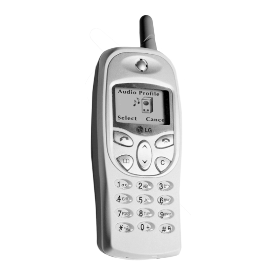
- Page 1 LG-200 SERVICE MANUAL...
-
Page 2: Table Of Contents
Table Of Contents ............. 1. PERFORMANCE 1-1. HW Features ............2 1-2. Memory Requirment ..........2 1.3. Technical Specification ........... 3 1-4. GSM band RF Specifications ......... 7 1-5. DCS band RF Specifications ........8 1-6. Receiver (GSM) ............9 1-7. -
Page 3: Performance
1. PERFORMANCE 1-1. HW Features Item Feature Comment Battery Li-Ion Battery, 600mAh Size : 105.9x44.8x19.7mm Weight : 89g, 77cc : M/B:99.5x38.3;K/B:99.5x39.4mm AVG TCVR current(mA) GSM Imax(390mA),DCS Imax(320mA) ≤ 5mA Stand by current(mA) - Talk time 2.5-hour (GSM Tx Level_7) - Stand by time 85-hour(Paging Period:2 RSSI:-85dBm) - Charging time 1.5-hour... -
Page 4: Technical Specification
1. PERFORMANCE 1-3. Technical Specification Item Description Specification Frequency Band GSM900 band Tx : 890 + n*0.2 MHz Rx : 935 + n*0.2 MHz (n = 1 ~ 124) GSM1800 band Tx : 1710 + (n-512)*0.2 Rx : 1805 + (n-512)*0.2 (n = 512 ~ 885) Phase error RMS <... - Page 5 Item Description Specification Spectrum due GSM900 to modulation Offset from Carrier(KHz). Max. dBc +0.5 600 ~ <1200 1200 ~ <1800 1800 ~ <3000 3000 ~ <6000 ≥ 6000 GSM1800 Offset from Carrier(KHz). Max. dBc +0.5 600 ~ <1200 1200 ~ <1800 1800 ~ <3000 3000 ~ <6000 ≥...
- Page 6 1. PERFORMANCE Item Description Specification Rx Level Report accuracy GSM900 GSM1800 ≥ -88 ≥ -86 ≥ -101 ≥ -99 < -101 < -99 8 ± 3 dB Sending Response Frequency (Hz) Max.(dB) Min.(dB) 1,000 2,000 3,000 3,400 4,000 2 ± 3 dB Receiving Response Frequency (Hz) Max.(dB)
- Page 7 Item Description Specification Power consumption Full power: < 390mA (GSM) ; < 320mA (DCS) Standby : 1. Normal ’≤ 5mA(Mix. power) 2. Using Test mode on DSP Sleep function ≤ 6mA Talk time GSM/ Level_7 (Battery Capacity 650mA): 130Min GSM/ Level_7 (Battery Capacity 600mA): 120Min Standby time Under conditions, at least 85 hours: 1.
-
Page 8: Gsm Band Rf Specifications
1. PERFORMANCE 1-4. GSM band RF Specifications Frequency Stability < ± 90Hz RF Maximum Power Output 33dBm RF Output Power Levels 15, decrementing in 2dB steps Power Control Level 5 33dBm ± 2dB Power Control Level 6 31dBm ± 3dB Power Control Level 7 29dBm ±... -
Page 9: Dcs Band Rf Specifications
1-5. DCS band RF Specifications Frequency Stability < ± 180Hz RF Maximum Power Output 30dBm RF Output Power Levels 16, decrementing in 2dB steps Power Control Level 0 30dBm ± 2dB Power Control Level 1 28dBm ± 3dB Power Control Level 2 26dBm ±... -
Page 10: Receiver (Gsm)
1. PERFORMANCE 1-6. Receiver (GSM) RX Frequency Input Low Channel (Ch 1) 935.2 MHz Mid Channel (Ch 62) 947.4 MHz High Channel (Ch 124) 959.8 MHz RX Frequency Calculation (F 935 + (ARFCN x 0.2) = F RX UHF VCO Frequency Low Channel (Ch 1) 1160-1230 MHz Mid Channel (Ch 62) -
Page 11: Technical Brief
2. TECHNICAL BRIEF 2-1. Receiver 1. The front end The RF receive signal (GSM 935Mhz - 960MHz, DCS 1805Mhz - 1880Mhz) is input via the antenna or coaxial connector. An antenna matching circuit is between the antenna and the connector. The diplexer U23 is used to control the Rx and Tx paths. - Page 12 2. TECHNICAL BRIEF 2. RX I&Q Demodulator The modulated IF signal is demodulated by mixing with a 270 MHz signal, which was derived from the 540Mhz oscillator. Before the mixer is a 32db gain IF amplifier which can be set to either 0 or 32db of gain.
- Page 13 3. UHF Synthesizer (Rx) The synthesizer for RX and TX UHF are implemented by W3000 (U19). The outputs of DCS VCO (1530 ~ 1610 MHz) and GSM VCO (1160 ~ 1230 MHz) are fed to U19 #5 for phase comparison in order to generate the charge pump output U19 #2 to control the frequency of VCOs.
- Page 14 2. TECHNICAL BRIEF 4. The Rx IF Synthesiser The major part of Rx IF synthesiser is built in W3020 including a phase comparator, and a charge pump, etc. Outside the W3020, the C164 and R189 and C225 form the loop filter; Q31 is a power switch and the VCO would be locked at 540 MHz.
-
Page 15: Transmitter
2-2. Transmitter [The TX IF Modulator in W3020] 1. The TX IF Modulator The TX I & Q signals from U1 #86-89 are fed to #38-41 of the W3020 TX modulator (U31), where they are then modulated onto either a TX IF of 270Mhz (for GSM-TX) or 180Mhz (for DCS-TX) by the quadrature-mixer inside U31. - Page 16 2. TECHNICAL BRIEF [The UHF Mixer/Amplifier/TX UHF Synthesiser] 3. The UHF Mixer Amplifier The modulated TX IF signal GSM (270Mhz) or DCS(180Mhz) is mixed onto the GSM(890Mhz-915Mhz) or DCS(1710Mhz-1785Mhz) TX RF frequency. This is achieved by mixing the TX IF signal with the TX UHF VCO output from U30 for GSM and U29 for DCS.
-
Page 17: The Pa Circuit
4. The TX UHF Synthesizer In TX mode the TX UHF VCO output is fed to #5 (U19) and then pre-scaled down to 200khz. The phase comparator within U19 compares this signal with a 200khz signal derived from the 13Mhz clock (U35) and outputs a current phase difference at #2. -
Page 18: The Pa Circuit And Its Control
2. TECHNICAL BRIEF 2-3. The PA Circuit and its Control 1. The PA Circuit and its Control The power amplifier control circuit ensures that the RF signal is regulated to the required limits of operation. Power-control is carried out according to the measurement of the power-output of the P.A. (RF_Detect, see Fig.: P.A Circuit Control). -
Page 19: 13 Mhz Clock
2-4. 13 MHz Clock The 13 MHz-clock (END3352B) consists of a TCXO (Temperature Compensated Crystal Oscillator) which oscillates at a frequency of 13MHz. It's used within the W3000 Synthesizers, Communication Protocol processor (CPP), and Super Chip 1 (SC1689). NC7S04 buffer the output to CPP, SC1 and W3000. - 18 -... -
Page 20: Main Processor And Dsp
2. TECHNICAL BRIEF 2-5. Main Processor and DSP 1. Main Processor CPP-C The CPP-C is a Lucent Technologies designed processor. The CPP-C performs the following functions: • CPU • CPU Interface • Interrupt Controller • Baseband Power Control • Keypad Control •... - Page 21 2. DSP and Mixed Signal Processor SC1689 Designed specifically for GSM cellular systems, the SC1689 (Super Chip 1) processor of Lucent Technologies is a mixed-signal device that is based on the DSP1600 core with a bit manipulation unit (BMU), error correction processor (ECCP), and conversion signal processor (CSP) core. The CSP consists of a baseband, voice band, and digital audio interface to fulfill the GSM requirement for a voice band and baseband interface.
-
Page 22: Power Supplies And Control Signals
2. TECHNICAL BRIEF 3. CPU Memories Flash ROM An 8Mbit programmable ROM is capable of being written while being still in circuit. Contains all the main command software for the mobile. SRAM A 128Kbit by 8 temporary memory device, which is used by CPP-C for CPU execution. 2-6. - Page 23 [Power supply] - 22 -...
-
Page 24: System Reset
2. TECHNICAL BRIEF 1. System Reset The R.C reset circuit generates a reset signal (active low) to the CPP-2 (SYS-RESET-B #77). when it detects that the VDD-DIG-ERROR-B active (Regulator 1,2 voltage is below the threshold of 2.85V- 0.5%) The device also reset CPP-2, this then holds the CPP-2 in reset mode, allowing only the real time clock to run. - Page 25 3. Battery Charge Control Charge control is composed of Q1, D1 D8-1, D8-2, Q4-2, Q5-1 and Q33. Charge control software controls the on/off of CHARGE-EN, which allows charge current to go through Q1-1 to battery cell. As the battery is fully charged, CHARGE-EN becomes low to stop fast charging. When the phone is off and the charger is plugged in, D7-3, Q4-1, and U38-6 form an auto-power-on circuit to turn on the phone..
- Page 26 2. TECHNICAL BRIEF 4. Real-Time Clock The real-time clock is driven by a 32.768 kHz clock from a crystal oscillator. The input clock is divided by 32,768 to generate a clock with a 1 second period that increase a 29-bit seconds counter. In addition, it can generate interrupts at a programmed time.
- Page 27 5. Vibrator The vibrator is driven by the signal VIBRATOR_EN, which is output from U58 (74VHC273). The signal is amplified by the transistor Q10 (2SC2411K) and is supplied from Vbat. - 26 -...
- Page 28 2. TECHNICAL BRIEF 6. Battery Voltage and Temperature Sensing The CPP can monitor the state of the battery through the battery interface connector J6. This can be done during both normal and charging operations. The battery provides a number of interface connections that enable the CPP determine the battery type, its capacity, temperature and whether it is possible to re-charge the cell(s).
-
Page 29: User Interface Board
2-7. User Interface Board 1. Keypad Switches and Scanning The key switches are metal domes, which make contact between two concentric pads on the top layer of the PCB when pressed. There are 18 switches (S1-18), connected in a matrix of 3 rows by 6 columns, as the figure shown above except for the power switch (S18), which is connected independently. -
Page 30: Display And Interface
2. TECHNICAL BRIEF 2. Display and Interface Power to the LCD is controlled by CPP and can be switched on and off via SYS_RESET_B. A high on this output powers the LCD; a low switches it off. There is also the control output LCD_CS1 that is also derived from CPP, this acts as the chip select enable for the LCD module. - Page 31 3. Microphone The microphone is mounted in the handset front cover and connects to User Interface Board. The audio signal is passed to User Interface Board and to the MICIN (#4) pin of SC1689. The voltage supply VREG is output from SC1689 #3, and is a bias voltage for both the MICP (through R8) and EXT_IN lines.
- Page 32 2. TECHNICAL BRIEF 5. Hands-free Interface The audio out (AOUTBP & AOUTBN) to the hands-free kit consists of a pair of differential signals from SC1689 auxiliary outputs (#95-96), which are tracked down the board to carkit connector (J5) at the base of the handset.
-
Page 33: Testing Set-Up And Checking Signals
7. Back-light Illumination In Back-light illumination, there are 10 green LEDs (six for keys and four for the LCD) in User interface Board, which are driven by BACKLIGHT_EN line from CPP. 2-8. Testing Set-up and Checking Signals 1. Receiver RF Levels and Checks This section shows the typical RF levels expected throughout the receiver path. - Page 34 2. TECHNICAL BRIEF 3. Testing Receiver Using a suitable high frequency probe measure the RF levels at the relevant points shown in Figure1 and compare your measurements with those shown in the diagram. If there are any major differences between the readings taken and those indicated then further investigation of that particular point will be required.
- Page 35 I Receiver RF Levels • DCS: Ch.699, -40dBm • GSM: Ch.62, -40dBm [Figure 1. Receiver Block Diagram] - 34 -...
- Page 36 2. TECHNICAL BRIEF I Transmitter RF Levels • GSM: Pwr Lvl 11, Ch.62, 21dBm • DCS: Pwr Lvl 5, Ch.699, 20dBm [Figure 2. Transmitter Block Diagram] - 35 -...
- Page 37 [Figure 3. Diplexer_Circuit] [Figure 4. System Clock] - 36 -...
- Page 38 2. TECHNICAL BRIEF [Figure 5. Power_Supply_Circuit] - 37 -...
- Page 39 [Figure 6. The control signal of Diplexer (see Fig.3)] [Figure 7. VDD_CPP (see Fig.5)] - 38 -...
- Page 40 2. TECHNICAL BRIEF [Figure 8. VDD_SC1 (see Fig.5)] [Figure 9. VDD_OSC (the Tx is unable) (see Fig.5)] - 39 -...
- Page 41 [Figure 10. VDD_OSC (the Tx is enable) (see Fig.5)] [Figure 11. VDD_RF (the Tx is unable) (see Fig.5)] - 40 -...
- Page 42 2. TECHNICAL BRIEF [Figure 12. VDD_RF (the Tx is enable) (see Fig.5)] [Figure 13. VDD_Tx_BUF (the Tx is unable) (see Fig.5)] - 41 -...
- Page 43 [Figure 14. VDD_Tx_BUF (the Tx is enable) (see Fig.5)] [Figure 15. TCXO (13MHz_RF) (see Fig.4)] - 42 -...
-
Page 44: Dimensions Of Main Components
2. TECHNICAL BRIEF 2-9. Dimensions of Main Components. • BZX84_C4V3 D1 [Voltage regulator diodes] • IMN10 D7 D8 D9 [Ultra high speed switching diode array] - 43 -... - Page 45 • BAT62-07W D5 [Silicon Schottky Diode] • LM4041CIM3-1.2 D6 [Precision Micropower Shunt Voltage Reference] - 44 -...
- Page 46 2. TECHNICAL BRIEF • BSS138 Q30 [SIPMOS Small-Signal Transistor] • BCR400W U40 [Active Bias Controller] - 45 -...
- Page 47 • UMX1N Q5 Q28 [General purpose transistor] • UMH11N Q27 [General purpose (dual digital transistors)] - 46 -...
- Page 48 2. TECHNICAL BRIEF • Si6923DQ Q1 [P-Ch 2.5-V (G-S) MOSFET With Schottky Diode] • UMB10N Q15 [General purpose (dual digital transistors)] - 47 -...
- Page 49 • Si2301DS Q21 Q22 [P-Channel 1.25-W, 2.5-V MOSFET] • UMA3N Q29 [Emitter common (dual digital transistors)] - 48 -...
- Page 50 2. TECHNICAL BRIEF • 2SA1576A Q33 [General Purpose Transistor] • DTA123JUA Q31 [Digital transistors (built-in resistors)] - 49 -...
- Page 51 [CPP U15] [SC1689 U1] - 50 -...
- Page 52 2. TECHNICAL BRIEF [W3020-ES3 U31] [W3000-ES3 U19] - 51 -...
- Page 53 [UCVE1X114A U42] - 52 -...
-
Page 54: Trouble Shooting
3. TROUBLE SHOOTING 3. TROUBLE SHOOTING 3-1. Power Supply Failure a) Failure: - Problem with turning on Mobile phone. ➜ Solution: 1. Test the set's current by using battery simulator; observe the value of current used. 2. Case1: If the current is higher 300mA, please C333 check C333. - Page 55 c) Failure/Solution: - If the value of current looks like short circuit, please replace U9 or U23. d) Failure/Solution: - Check the voltage output of Pin1 of U41; the value should between 2.8V and 3.5. - Please replace U41 or U39 if there is no output or value abnormal.
-
Page 56: Voice Function Failure
3. TROUBLE SHOOTING 3-2. Voice Function Failure a) Failure: - Microphone voice failure. ➜ Solution: - Test the resistance of C18 capacitor by using multi-meter. Replace C18 if the testing value is lower than 18Ω. - Replace Microphone if C18 is fine. b) Failure: - Hand free function failure ➜... - Page 57 c) Failure: - No Back Light ➜ Solution: - Replace the LED that doesn't light up including any failing parts of LED. - If all of LEDs fail, please check whether J1 has cold solder. - Check the circuit trace on UIF board. d) Failure: - Fails on Dark display;...
-
Page 58: Transmission & Receiving Failure
3. TROUBLE SHOOTING 3-4. Transmission & Receiving Failure a) Failure: - Receiving signal failure ➜ Solution: - Check the soldering of U23, U31. - Otherwise replace U23, U31. b) Failure: - Transmission signal failure ➜ Solution: - Check the soldering of U23, U9, and U32. - Otherwise, replace U23, U9, and U32. - Page 59 d) Failure: - No Buzzer sound ➜ Solution: - Check the soldering of J1. - Check the trace insulator around screw hole on the UIF board. e) Failure: Key light failure ➜ Solution: - If any parts of LEDs are not working, please replace them with new LED.
- Page 60 3. TROUBLE SHOOTING f) Failure: - Problem with inserting card message ➜ Solution: - Replace C6 capacitor if its resistance is from end to end is between 1Ω and 25Ω. - If C6 is fine, please replace U11. g) Failure: - Clock is not working ➜...
-
Page 61: Test Point Data
4. TEST POINT DATA I LG200 M/B (1-1) - 60 -... - Page 62 4. TEST POINT DATA I Component list of LG200 M/B (1-2) Location LG-200 M/B(1-2) 2.9V Voltage comparator Provide SIM card power (3V ,5V) SIM LOCK SC 1689 Provide power for U1(SC1689) V =3.8V =2.85V Provide power for POWER Control Loop V =3.8V V...
- Page 63 I LG200 M/B (2-1) - 62 -...
- Page 64 4. TEST POINT DATA I Component list of LG200 M/B (2-2) Location LG-200 M/B(2-2) SC1689 measure : V of PIN2,10,21,25,36,49,54,58,66,68,71,85,92 = 2.85V Frequency of PIN59.60 = 13MHz SC1699 power measures : V of PIN1 = 3.8V, PIN3 = High, V of PIN5 = 2.85V...
- Page 65 I LG-200 M/B (3-1) - 64 -...
- Page 66 4. TEST POINT DATA I Component list of LG-200 M/B(3-2) Location LG-200 M/B(3-2) Local OSC Vco,540MHz DCS receive filter GSM receive filter DCS transmit filter DCS transmit-couple circuit GSM transmit filter RF signal processor, for failure during network service or receiving/transmiting data...
- Page 67 I LG-200 M/B (4-1) - 66 -...
- Page 68 4. TEST POINT DATA LG-200 M/B(4-2) Local OSC measures; PIN1 = 2.85V; PIN6 = 540MHz at receive/transmit mode GSM RX filter DCS TX filter measures; PIN2 = -21.5dBm, PIN6 = -24.33dBm GSM TX filter measures; PIN2 = -9.07dBm, PIN3 = -8.07dBm W3020(RF signal processor) measures;...
-
Page 69: Assembly Instructions
5. ASSEMBLY INSTRUCTIONS 1. Remove battery pack 2. Remove screws There are 4 screws in total - 68 -... - Page 70 5. ASSEMBLY INSTRUCTIONS 3. Turn handset up 4. Take off front panel - 69 -...
- Page 71 5. Take off keypad 6. Remove screws There are 2 screws in total - 70 -...
- Page 72 5. ASSEMBLY INSTRUCTIONS 7. Take off UIF board 8. Take off shielding cover - 71 -...
- Page 73 9. Take off main board 10. Disconnect the Vibrator connector - 72 -...
-
Page 74: Block Diagram
6. BLOCK DIAGRAM 6. BLOCK DIAGRAM - 73 -... -
Page 75: Circuit Diagram
7. CIRCUIT DIAGRAM • POWER SUPPLY - 74 -... - Page 76 7. CIRCUIT DIAGRAM • MCU & MEMORY - 75 -...
- Page 77 • SCI - 76 -...
- Page 78 7. CIRCUIT DIAGRAM • RF CORE - 77 -...
- Page 79 • RF FRONT END - 78 -...
- Page 80 7. CIRCUIT DIAGRAM • POWER CONTROL LOOP - 79 -...
- Page 81 • MISC - 80 -...
- Page 82 7. CIRCUIT DIAGRAM • CARKIT CONNECTOR - 81 -...
- Page 83 - 82 -...
-
Page 84: How To Download S/W
8. HOW TO DOWNLOAD S/W 8. HOW TO DOWNLOAD S/W 1) Select optiflash.exe from 'flash' file 2) Connect a data cable to the phone • Select settings in the main screen • Select either com port: 1 or com port: 2 •... -
Page 85: How To Process Calibration
9. HOW TO PROCESS CALIBRATION 9-1. Equipment Lists Equipment for Calibration Type / Model Brand Wireless Communication Test Set HP-8960 Hewlett Packard RS232 Connector (for Software Installation) RF Cable Power Supply HP-66311B Hewlett Packard GBIP interface card HP-GBIP Hewlett Packard Test SIM Card ORGA Hewlett Packard... - Page 86 2. Install Battery simulator on handset 3. Connect RS-232 Cable to connector on handset 4. Connect RF Cable to LG-200 handse’s RF Connector 5. POWER ON PC then enter into WINDOWS NT. (Remark: Windows 95, 98, 2000 system could be feasible, but we strongly recommend using Windows NT system due to stability reason) 6.
- Page 87 7. Select CAL item. 8. Select RUN Icon, start the Calibration process. (Processing Screen) - 86 -...
- Page 88 9. HOW TO PROCESS CALIBRATION 9. The program will be stopped automatically when process finish. (Finished Screen) - 87 -...
- Page 89 9-4. GSM900/DCS1800 Calibration Test Flowchart GSM900 DCS1800 Battery Fetch TX Calibration Channel & Level Original Call LAN Calibration Read RX Load Default Channel & Level Fetch TX END CALL Channel & Level LNA and IF Calibration ERROR MESSAGE 1) Try the process once more Read RX 2) Download S/W and try...
- Page 90 9. HOW TO PROCESS CALIBRATION 9-5. GSM900/DCS1800 Final Test Flowchart Original Call Test GSM Change Item: TXP, PVT PFER, ORFS- Channel MO, ORFS-SW, FBER, RXL, GSM900 Cannel&Level End of GSM900 Test Change Test DCS Channel Items: TXP, PVT PFER, ORFS-MO, ORFS- SW, FBER, RXL, RXQ.
-
Page 91: Exploded View
10. EXPLODED VIEW - 90 -... -
Page 92: Replacement Parts List
11. REPLACEMENT PARTS LIST 11. REPLACEMENT PARTS LIST 1) Main Board LTEM PART NO. LOCATION SPECIFICATION REMARK GM447052J0 C1,C2,C65,C66,C67,C69,C70,C71,C85,C86,C113, CHIP MONO 1608 47P/50V JN MURATA C114,C115,C116,C117,C120,C127,C146,C154,C155, C157,C302,C304,C305,C330 GM433052J0 C3,C5,C23,C27,C33,C44,C53,C56,C57,C170,C172, CHIP MONO 1608 33P/50V JN MURATA C254,C273,C291,C311,C324,C364 GM04751870 C6,C135 CHIP MONO 2012 4.7U/10V ZY TATYO YUDEN GM410423J0 C7,C8,C9,C10,C11,C12,C63,C73,C74,C75,C76,C77, CHIP MONO 1608 0.1U/16V KX MURATA... - Page 93 LTEM PART NO. LOCATION SPECIFICATION REMARK GM422052J0 C196,C197,C243,C258,C259,C357 CHIP MONO 1608 22P/50V JNMURATA GM410052J0 C214,C216 CHIP MONO 1608 10P/50V JN MURATA GM127252J0 C225 CHIP MONO 3216 0.0027U/50V JNCOG MURATA GM40805BJ0 C233 CHIP MONO 1608 8P/50V CNMURATA GM447333J0 C242,C329 CHIP MONO 1608 0.047U/25V KX MURATA GM40405BJ0 C245,C283 CHIP MONO 1608 4P/50V CNMURATA...
- Page 94 11. REPLACEMENT PARTS LIST LTEM PART NO. LOCATION SPECIFICATION REMARK HD000021S0 L63,L64,L65,L79 CORE SMT 68nH 0603 5% KOA HB100142E0 COIL SMT 5.45nH 0906 5% COILCRAFT EG950001T0 MOSFET-P-SCH SI6923DQ TSSOP 8PVISHAY EA95853040 TR NPN UMH10N SC-88 6P ROHM EA95000440 Q5,Q20,Q28 TR NPN UMX1N UM6 6P ROHM EA95000740 TR NPN 2SC2411K SMT 3P ROHM EG92000430...
- Page 95 LTEM PART NO. LOCATION SPECIFICATION REMARK FN01100400 R121,R123,R124,R248 CHIP RES 1/10W 1% 1M 1608 FN01056000 R126 CHIP RES 1/10W 1% 56ohm 1608 FM01033900 R128 CHIP RES 1/10W 5% 3.3ohm 1608 FN01120300 R129 CHIP RES 1/10W 1% 120K 1608 FN01120200 R131,R189 CHIP RES 1/10W 1% 12K 1608 FN01470200 R130,R259...
- Page 96 11. REPLACEMENT PARTS LIST LTEM PART NO. LOCATION SPECIFICATION REMARK AR10140310 IC TC74VHC14FT TSSOP 14PTOSHIBA AR11320310 IC TC74VHC132FT TSSOP 14PTOSHIBA DE03520Y80 L-VOLT DET RN5VT29 SOT23 5P RICOH EN460008Y0 VCO-IF UCVE1X114A-540MHz SMD JZ040002Z0 FILTER-RF B4686 SMD 6P SIEMENS JZ040008Z0 FILTER-RF B4693 SMD 8P SIEMENS AR10245310 IC TC74VHC245FT TSSOP 20PTOSHIBA HA03203750...
- Page 97 2) Keyboard LTEM PART NO. LOCATION SPECIFICATION REMARK HJ02004760 BUZZER SMT-8103C SMD SAMBU GM410423J0 C901,C915,C916,C925 CHIP MONO 1608 0.1U/16V KX MURATA GM410152J0 C902,C920 CHIP MONO 1608 100P/50V JN MURATA GM03351870 C903,C904,C905,C906 CHIP MONO 2012 3.3U/10V ZY TAIYO YUDEN GM410518J0 C907,C908,C909,C910,C911 CHIP MONO 1608 1U/10V ZY MURATA GM610152J0 C912,C913,C914...
- Page 98 11. REPLACEMENT PARTS LIST 3) Mechanical/Electrical/Packing Parts Item Part No. Specification Remark R393000930 Antenna (Black) R3870068A0 LCD Lens (In-Mold Grey) R395003660 Adhesive Tape for LCD Lens R3920024J0 Keypad (Silver White P+R) R401000260 Metal Dome for Keypad R2710150B0 Upper Case - Pearl White R2710209B0 Upper Case - Dark Silver R2710213B0...
- Page 99 4) STANDARD ACCESSORIES Item Part No. Specification JB040042A0 Battery Pack - 600mAh Li-Ion JB100083E0 Switching Travel Charger - Europe Version (Round Pin) 5) OPTIONAL ACCESSORIES Item Part No. Specification Headset Cigar Lighter Charger Mock up (Dummy) Simple Handsfree Car Kit Cable (for S/W Upgrading) Cable (for RF Testing) - 98 -...
Need help?
Do you have a question about the LG-200 and is the answer not in the manual?
Questions and answers