Table of Contents
Advertisement
Quick Links
SERVICE MANUAL
Dolby noise reduction manufactured under license from Dolby Labo-
ratories Licensing Corporation.
"DOLBY" and the double-D symbol a are trademarks of Dolby
Laboratories Licensing Corporation.
AUDIO POWER SPECIFICATIONS (US Model)
POWER OUTPUT AND TOTAL HARMONIC DISTORTION
13 watts per channel minimum continuous average power into
4 ohms, 4 channels driven from 20 Hz to 20 kHz with no more
than 1% total harmonic distortion.
Other Specifications
CD player section
Signal-to-noise ratio
94 dB
Frequency response
5 – 20,000 Hz
Wow and flutter
Below measurable limit
Laser Diode Properties
Material
GaAlAs
Wavelength
780 nm
Emission Duration
Continuous
Laser output power
Less than 44.6 µW*
* This output is the value measured at a distance
of 200 mm from the objective lens surface on
the Optical Pick-up Block.
Cassette player section
Tape track
4-track 2-channel stereo
Wow and flutter
0.08 % (WRMS)
Frequency response
30 – 20,000 Hz
Signal-to-noise ratio
Cassette type
Dolby B NR
TYPE II, IV
67 dB
TYPE I
64 dB
MICROFILM
SPECIFICATIONS
Dolby NR off
58 dB
55 dB
CHANGER CONTROL AUDIO MASTER
WX-C55
Model Name Using Similar Mechanism
CD
CD Drive Mechanism Type
Section
Optical Pick-up Name
Model Name Using Similar Mechanism
TC
Section
Tape Transport Mechanism Type
Tuner section
FM
Tuning range
US model:
87.5 – 107.9 MHz
E model:
FM tuning interval:
50 kHz/200 kHz switchable
87.5 – 108.0 MHz
(at 50 kHz step)
87.5 – 107.9 MHz
(at 200 kHz step)
Antenna terminal
External antenna connector
Intermediate frequency 10.7 MHz
Usable sensitivity
9 dBf
Selectivity
75 dB at 400 kHz
Signal-to-noise ratio
65 dB (stereo),
68 dB (mono)
Harmonic distortion at 1 kHz
0.7% (stereo),
0.4% (mono)
Separation
35 dB at 1 kHz
Frequency response
30 – 15,000 Hz
US Model
E Model
NEW
MG-378X-121
KSS-521A
XR-C8820
MG-25E-136
– Continued on next page –
1
Advertisement
Chapters
Table of Contents

Related Manuals for Sony WX-C55


Summary of Contents for Sony WX-C55
- Page 1 WX-C55 SERVICE MANUAL US Model E Model Dolby noise reduction manufactured under license from Dolby Labo- Model Name Using Similar Mechanism ratories Licensing Corporation. CD Drive Mechanism Type MG-378X-121 “DOLBY” and the double-D symbol a are trademarks of Dolby Section...
- Page 2 COMPONENTS IDENTIFIED BY MARK ! OR DOTTED LINE WITH MARK ! ON THE SCHEMATIC DIAGRAMS AND IN THE PARTS LIST ARE CRITICAL TO SAFE OPERATION. REPLACE THESE COMPONENTS WITH SONY PARTS WHOSE PART NUMBERS APPEAR AS SHOWN IN THIS MANUAL OR IN SUPPLEMENTS PUBLISHED BY SONY.
-
Page 3: Table Of Contents
TABLE OF CONTENTS 1. GENERAL 5. ELECTRICAL ADJUSTMENTS Location of Controls ............... 4 Tape Section ................. 20 Getting Started ................ 4 Tuner Section ................ 21 CD Player ................4 CD Section ................24 Cassette Player ............... 5 Radio ..................5 6. -
Page 4: General
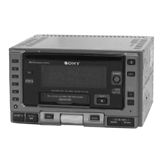
SECTION 1 GENERAL This section extracted from instruction manual. -
Page 10: Disassembly
SECTION 2 DISASSEMBLY Note : Follow the disassembly procedure in the numerical order given. 2-1. COVER 1 PTT 2.6x5 3 cover 2 claws 2-2. FRONT PANEL ASSY 1 PTT 2.6x5 3 claw 7 CN501 5 CN801 4 claw 6 CN500 8 front panel assy 2 PTT 2.6x5... -
Page 11: Cd Mechanism Block
2-3. CD MECHANISM BLOCK 5 bracket (CD) 4 PTT 2.6x5 3 CD mechanism block 2 CN802 1 PTT 2.6x5 2-4. TR BOARD, HEAT SINK 4 CN901 9 heat sink 8 PTT 2.6x12 3 TR board 7 PTT 2.6x12 1 PTT 2.6x12 6 PTT 2.6x12 2 cover (DD converter) 5 PTT 2.6x12... -
Page 12: Cd Board
2-5. CD BOARD 4 PTT 2.6x6 3 PTT 2.6x6 1 CN803 2 CN402 5 CD board 6 insulating sheet (L) 2-6. CHASSIS (U) 4 chassis (U) 2 PTT 2.6x5 1 PTT 2.6x5 3 PTT 2.6x5... -
Page 13: Tape Mechanism Block
2-7. TAPE MECHANISM BLOCK 2 PTT 2.6x5 5 tape mechanism block 4 CN300 3 CN600 1 PTT 2.6x5 2-8. MAIN BOARD 2 PTT 2.6x6 1 PTT 2.6x6 3 MAIN board 4 insulating sheet (L) -
Page 14: Chassis (Tm) Assy
2-9. CHASSIS (TM) ASSY 6 chassis (TM) assy 1 P 2x3 2 P 2x3 3 P 2x3 4 claw 5 CN4 2-10. SENSOR BOARD 1 claw 3 guide (DISC M) 2 claw 4 PS 2x3 5 SENSOR board... -
Page 15: Servo Board
2-11. SERVO BOARD 8 PS 2x4 7 PS 2x4 4 wires 2 CN2 3 Removal the two solders. 1 CN3 9 SERVO board 5 P 2x3 6 loading motor assy 2-12. ROLLER ASSY • When installing, take note of the positions arm (roller) and washers. -
Page 16: Chassis (Op) (O/S) Assy
2-13. CHASSIS (OP) (O/S) ASSY 6 chassis (OP) (O/S) assy 8 compression spring (FL) 1 tension spring (KF8) 7 compression spring (FL) 4 Fit lever (D) in the direction of the arrow. 5 Turn loading ring in the direction of the arrow. 3 damper (T) 2 damper (T) 2-14. -
Page 17: Assembly Of Mechanism Deck
SECTION 3 ASSEMBLY OF MECHANISM DECK Note : Follow the assembly procedure in the numerical order given. 3-1. HOUSING 7 Holder the hanger by bending the claw. 5 Fit projection on C part. 1 Install the catcher to the hanger. 2 Install the hanger onto two claws of the housing. -
Page 18: Lever (Ldg-A)/(Ldg-B)
3-3. LEVER (LDG-A) / (LDG-B) shaft A shaft A shaft B shaft C shaft B 1 Fit the lever (LDG-A) on shafts A to C and install it. 3 type-E stop ring 2.0 2 Fit the lever (LDG-B) on shafts A and B and install it. 3-4. -
Page 19: Guide (C)
3-5. GUIDE (C) 2 guide (C) 1 claws 3-6. CAPSTAN / REEL MOTOR (M904) 3 belt (25) 2 precision screws P 2x3 1 main motor assy (CAPSTAN/REEL) (M904) 30 °... -
Page 20: Mechanical Adjustments
SECTION 4 MECHANICAL ADJUSTMENTS PRECAUTION See the adjustment location from on page 23 for the 1. Wipe the following components with an absorbent cotton cloth adjustment. moistened with alcohol before adjustment : PB head Pinch roller 0 dB = 0.775 V TAPE SECTION Idler Rubber belt... -
Page 21: Tuner Section
TUNER SECTION 0 dB = 1 µV FM Stereo Separation Adjustment Setting : SOURCE button : FM Cautions during repair FREQUENCY SELECT switch (E model) : FM 200k When the tuner unit is defective, replace it by a new one because its internal block is difficult to repair. - Page 22 AM Auto Scan/Stop Level Adjustment Note : This adjustment should be performed after the FM Auto Scan / Stop Level Adjustment is done. Setting : SOURCE n MODE button : AM FREQUENCY SELECT switch (E model) : AM 10k 30 Ω 15 pF 65 pF AM RF signal...
- Page 23 Adjustment Location : – set lower view – RV200 TP-R (R-CH) DOLBY LEVEL DOLBY LEVEL TP-L RV100 (L-CH) – set upper view – TAPE SPEED ADJ RV1 AM AUTO SCAN/STOP LEVEL ADJ RV2 FM AUTO SCAN/STOP LEVEL ADJ RV200 (R-CH) DOLBY LEVEL ADJ RV4 FM STEREO SEPARATION ADJ RV100 (L-CH) DOLBY LEVEL ADJ...
-
Page 24: Cd Section
CD SECTION Focus Gain Adjustment (Coarse adjustment) This adjustment is not required unless the following parts are replaced: Note : • Optical pick-up 1. CD Block basically constructed to operate without adjustment. • Therefore, check each item in order given. 2. -
Page 25: Diagrams
SECTION 6 DIAGRAMS 6-1. IC PIN DESCRIPTIONS • IC500 µPD78058GC-B51-8BT (SYSTEM CONTROL) Pin No. Pin Name Pin Description FM, AM common signal meter A/D conversion input Not used. (Connect to ground in this set.) SD-IN Station detecter input (“H” : with SD) AVSS —... - Page 26 Pin No. Pin Name Pin Description SYS-RST System reset signal output BUS-ON Bus ON control output 56, 57 RE1, 0 Rotary encoder input 1, 0 AD-ON Power supply output for A/D conversion. RAMBU RAM reset detection input RESET — Reset input SIRCS Remote control input (Not used in this set.) BU-IN...
- Page 27 • IC801 µPD78054GC-A32-8BT (CD SYSTEM CONTROL) Pin No. Pin Name Pin Description LEDCLK — Not used in this set. LEDCKO — Not used in this set. LEDSO — Not used in this set. AVSS — Analog ground FL-CE0 Display driver chip select output 0 FL-CE1 Display driver chip select output 1 (Not used in this set.) AVREF1...
- Page 28 Pin No. Pin Name Pin Description EESIO Not used in this set. EECKO Not used in this set. RESET — Reset input SCOR SCOR signal detection input CNIN Track jump count input SELF-SW Disc self store detection input SENS SENS signal detection input DQSY —...
-
Page 29: Block Diagram -Cd Section
WX-C55 6-2. BLOCK DIAGRAM — CD SECTION — OPTICAL PICK-UP RF AMP, SERVO CONTROL DIGITAL SIGNAL PROCESSOR D/A CONVERTER KSS-521A IC401 MAIN 35 PD1 14 RF PCMD DATA LOUT SECTION LRCK 36 PD2 59 CLKO 4 LRCK ROUT R-CH I - V... -
Page 30: Block Diagram -Tape Section
WX-C55 6-3. BLOCK DIAGRAM — TAPE SECTION — (Page 31) MAIN SECTION TAPE EQ/DOLBY NR SYSTEM CONTROL CD SYSTEM CONTROL FL DRIVER IC500 ( 2/2 ) IC801 ( 2/2 ) IC300 IC701 HP901 SA CONTROL PLAYBACK HEAD FWD/REV IC802 MTL/NORMAL... -
Page 31: Block Diagram -Main Section
WX-C55 6-4. BLOCK DIAGRAM — MAIN SECTION — REAR R-CH CN401(2/2) AUDIO OUT FRONT R-CH POWER AMP ELECTRONIC VOLUME IC751 CN651 CN401(1/2) IC350 BUS AUDIO IN –2 TUNER INIT R-CH FL IN FL– –1 Q180 FL– IC331 (ANTENNA) ANT AM L-CH OUT... -
Page 32: Circuit Boards Location
• Semiconductor 6-5. CIRCUIT BOARDS LOCATION THIS NOTE IS COMMON FOR PRINTED WIRING BOARDS Location AND SCHEMATIC DIAGRAMS. (SERVO Board) (In addition to this, the necessary note is Ref. No. Location printed in each block.) Note on Printed Wiring Boards: •... -
Page 33: Printed Wiring Boards -Cd Mechanism Section
WX-C55 6-6. PRINTED WIRING BOARDS — CD MECHANISM SECTION — (Page 36) -
Page 34: Schematic Diagram -Cd Mechanism Section (1/2)
WX-C55 6-7. SCHEMATIC DIAGRAM — CD MECHANISM SECTION (1/2) — • Refer to page 35 for Waveforms and page 48 for IC Block Diagrams. Note: • Voltage and waveforms are dc with respect to ground under no-signal conditions. no mark : CD PLAY ∗... -
Page 35: Schematic Diagram -Cd Mechanism Section (2/2)
WX-C55 6-8. SCHEMATIC DIAGRAM — CD MECHANISM SECTION (2/2) — • Refer to page 48 for IC Block Diagrams. • Waveforms (MODE : CD PLAY) Approx. 620mVp-p (FEO) 1.2Vp-p #¡ (RFO) Approx. 200mVp-p $™ (TEO) 2.6Vp-p 7.6µsec (MDP) 5.8Vp-p 22.7µsec @º... -
Page 36: Printed Wiring Board -Tr Section
WX-C55 6-9. PRINTED WIRING BOARD — TR SECTION — 6-11. PRINTED WIRING BOARD — CD SECTION — (Page 38) (Page 39) 6-10. SCHEMATIC DIAGRAM — TR SECTION — (Page 37) • Semiconductor Location (CD board) Ref. No. Location (Page 37) -
Page 37: Schematic Diagram -Cd Section
WX-C55 6-12. SCHEMATIC DIAGRAM — CD SECTION — • Refer to page 51 for IC Block Diagrams. (Page 41) (Page 36) (Page 41) (Page 36) (Page 35) (Page 46) Note: • Voltage is dc with respect to ground under no-signal condition. -
Page 38: Printed Wiring Board -Main Section
WX-C55 6-13. PRINTED WIRING BOARD — MAIN SECTION — (Page 36) • Semiconductor Location Ref. No. Location Ref. No. Location (D1) F-11 D755 (D500) D756 (D501) D757 D758 (D502) (D503) D504 E-11 D505 IC300 H-10 D506 B-12 IC331 J-11 D507... - Page 39 WX-C55 (Page 36) (Page 45) (Page 47)
-
Page 40: Schematic Diagram -Main Section (1/4)
WX-C55 6-14. SCHEMATIC DIAGRAM — MAIN SECTION (1/4) — • Refer to page 50 for IC Block Diagrams. (Page 42) Note: • Voltage is dc with respect to ground under no-signal condition. no mark : FM ) : AM... -
Page 41: Schematic Diagram -Main Section (2/4)
WX-C55 6-15. SCHEMATIC DIAGRAM — MAIN SECTION (2/4) — (Page 37) (Page 37) Note: • Voltage is dc with respect to ground under no-signal (detuned) condition. (Page 42) (Page 43) no mark : FM... -
Page 42: Schematic Diagram -Main Section (3/4)
WX-C55 6-16. SCHEMATIC DIAGRAM — MAIN SECTION (3/4) — • Refer to page 50 for IC Block Diagrams. (Page 40) (Page 41) Note: • Voltage is dc with respect to ground under no-signal condition. no mark : FM ) : TAPE PLAY... -
Page 43: Schematic Diagram -Main Section (4/4)
WX-C55 6-17. SCHEMATIC DIAGRAM — MAIN SECTION (4/4) — • Refer to page 50 for IC Block Diagrams. (Page 41) (Page 47) (Page 46) Note: • Voltage is dc with respect to ground under no-signal condition. no mark : FM... -
Page 44: Printed Wiring Board -Control Section
WX-C55 6-18. PRINTED WIRING BOARD — CONTROL SECTION — • Semiconductor Location Ref. No. Location Ref. No. Location (D701) (IC701) (D704) C-10 (D705) C-10 (Q701) (D706) (Q702) C-10 D730 (Q703) D-10 D731 (Q704) D732 D733 B-12 ) : SIDE B... - Page 45 WX-C55 (Page 36) (Page 39)
-
Page 46: Schematic Diagram -Control Section
WX-C55 6-19. SCHEMATIC DIAGRAM — CONTROL SECTION — (Page 37) (Page 43) Note: • Voltage is dc with respect to ground under no-signal (detuned) condition. no mark : FM... -
Page 47: Printed Wiring Board -Jog Section
WX-C55 6-20. PRINTED WIRING BOARD — JOG SECTION — (Page 39) 6-21. SCHEMATIC DIAGRAM — JOG SECTION — (Page 43) -
Page 48: Ic Block Diagrams
• IC Block Diagrams IC1 CXD2507AQ (SERVO BOARD) SERVO AUTO SEQUENCER DATA XRST SENS SUB CODE MUTE PROCESSOR INTERFACE SQCK DIGITAL LOCK SQSO TEST EXCK SBSO FILO SCOR DIGITAL FILI DEMODULATOR WFCK EMPH AVSS CLTV ASYMMETRY AVDD CORRECTOR DIGITAL DOUT INTERFACE BIAS ERROR... - Page 49 IC2 CXA1782BQ 27 26 25 LEVEL S MIRR SENS RF IV AMP1 DFCT C.OUT XRST RF IV AMP2 FE BIAS IIL DATA REGISTER INPUT SHIFT REGISTER DATA ADDRESS DECODER OUTPUT DECODER TOG1-3 FS1-4 TG1-2 TM1-7 PS1-4 F IV AMP BAL1-3 FZC COMP E IV AMP TE AMP...
- Page 50 IC1 BU2624FV (MAIN BOARD) IC331, 341 NJM4558M XOUT PHASE A OUT B OUT REFERENCE – DIVIDER A IN– MAIN FMIN + – PRESCALER COUNT A IN+ B IN– B IN+ SHIFT REGISTER LATCH AMIN IF COUNT 20BIT COUNT IFIN IC300 CXA2510AQ IC620 BA8270F 120µ/ 70µ...
- Page 51 IC350 LC75374E LFIN – LFOUT – – – – LSELO LROUT – – VREF CONTROL – SHIFT – DECODER LATCH REGISTER RROUT RSELO – – – – RFOUT – RFIN 6 7 8 9 10 IC502 RN5VD23AA-TL IC401 PCM1717E-ST2 CLKO DGND CONTROL VREF...
- Page 52 IC802 BA3834F MULTIPLEXER DECODER REGISTER REGISTER REGISTER REGISTER REGISTER REGISTER REGISTER PEAK PEAK PEAK PEAK PEAK PEAK PEAK HOLD HOLD HOLD HOLD HOLD HOLD HOLD 68Hz 1kHz 2.4kHz 170Hz 420Hz 5.9kHz 14.4kHz B.P.F. B.P.F. B.P.F. B.P.F. B.P.F. B.P.F. B.P.F. DIFFERENTIAL AMPLIFIER 1 2 3 4 IC680 BA3918-V2...
-
Page 53: Exploded Views
SECTION 7 EXPLODED VIEWS NOTE: • The mechanical parts with no reference • -XX and -X mean standardized parts, so • Accessories and packing materials and number in the exploded views are not supplied. they may have some difference from the hardware (# mark) list are given in •... -
Page 54: Front Panel Section
7-2. FRONT PANEL SECTION FL701 VR771 Ref. No. Part No. Description Remark Ref. No. Part No. Description Remark 3-036-193-01 PANEL (VOL) 3-036-182-01 DOOR, CASSETTE 3-036-185-01 PLATE (VOL), LIGHT GUIDE 3-036-183-01 PLATE (CASSETTE), LIGHT GUIDE 3-029-975-01 SCREW (2X8), +P TITE 3-036-186-01 BUTTON (D-BASS) * 54 1-673-785-12 JOG BOARD 3-036-181-01 BUTTON (OFF) -
Page 55: Chassis Section
7-3. CHASSIS SECTION MG-378X-121 MG-25E-136 Ref. No. Part No. Description Remark Ref. No. Part No. Description Remark * 101 3-024-109-12 BRACKET (CD) * 109 A-3294-683-A MAIN BOARD, COMPLETE (US) 3-376-464-11 SCREW (+PTT 2.6X6), GROUND POINT * 109 A-3294-684-A MAIN BOARD, COMPLETE (E) * 103 3-024-107-11 BRACKET (U) * 110... -
Page 56: Tape Mechanism Section
7-4. TAPE MECHANISM SECTION (MG-25E-136) HP901 M904 not supplied Ref. No. Part No. Description Remark Ref. No. Part No. Description Remark A-3291-667-A CLUTCH (FR) ASSY 3-933-346-01 CATCHER * 152 3-019-130-01 LEVER (LDG-A) 3-933-344-01 GUIDE (C) 3-019-131-01 LEVER (LDG-B) 3-014-798-01 SCREW (HEAD), SPECIAL 3-020-539-01 SPRING (LD-1), TENSION 3-364-151-01 WASHER 3-020-540-01 SPRING (LD-2), TENSION... -
Page 57: Cd Mechanism Section (1)
7-5. CD MECHANISM SECTION (1) (MG-378X-121) M903 Ref. No. Part No. Description Remark Ref. No. Part No. Description Remark X-3376-767-1 CHASSIS (TM) ASSY 3-321-813-01 WASHER, COTTER POLYETHYLENE * 202 1-660-797-21 SENSOR BOARD 3-025-419-01 ARM (ROLLER) 3-032-474-01 GUIDE (DISC M) 3-937-561-01 SPRING (RA-E), TENSION 3-338-737-01 SCREW (2X3), +PS * 212 A-3313-563-A SERVO BOARD, COMPLETE... -
Page 58: Cd Mechanism Section (2)
7-6. CD MECHANISM SECTION (2) (MG-378X-121) Ref. No. Part No. Description Remark Ref. No. Part No. Description Remark X-3372-203-1 ARM ASSY, CHUCKING 3-014-727-01 WHEEL (LW), WORM 3-931-894-01 BRACKET (CP) 3-931-881-01 LEVER (LOCK) * 253 3-384-918-01 RETAINER (DISC) 3-935-828-01 LEVER (D) 3-021-326-01 SPRING (8) 3-931-882-02 GEAR (MDL) 3-931-895-11 SPRING (CH), TENSION... -
Page 59: Cd Mechanism Section (3)
7-7. CD MECHANISM SECTION (3) (MG-378X-121) M901 M902 The components identified by mark ! or dotted line with mark. ! are critical for safety. Replace only with part number specified. Ref. No. Part No. Description Remark Ref. No. Part No. Description Remark X-3372-205-2 CHASSIS (OP) (O/S) ASSY... -
Page 60: Electrical Parts List
SECTION 8 ELECTRICAL PARTS LIST NOTE: • Due to standardization, replacements in • Items marked “*” are not stocked since The components identified by mark ! or dotted line with mark. the parts list may be different from the they are seldom required for routine service. parts specified in the diagrams or the Some delay should be anticipated ! are critical for safety. -
Page 61: Description Remark Ref. No
Ref. No. Part No. Description Remark Ref. No. Part No. Description Remark D858 8-719-110-17 DIODE MA4100-L(TA) R402 1-216-037-00 METAL CHIP 1/10W D859 8-719-911-19 DIODE 1SS119-25TD R411 1-216-049-11 RES,CHIP 1/10W D860 8-719-053-18 DIODE 1SR154-400TE-25 R412 1-216-296-00 SHORT D862 8-719-053-18 DIODE 1SR154-400TE-25 R421 1-216-049-11 RES,CHIP 1/10W... - Page 62 CONTROL Ref. No. Part No. Description Remark Ref. No. Part No. Description Remark R853 1-249-417-11 CARBON 1/4W LSW711 1-762-618-21 SWITCH, KEY BOARD (WITH LED) (1) R854 1-249-417-11 CARBON 1/4W LSW721 1-762-618-21 SWITCH, KEY BOARD (WITH LED) (OFF) R855 1-249-421-11 CARBON 2.2K 1/4W LSW722 1-762-618-21 SWITCH, KEY BOARD (WITH LED) (CD 6)
- Page 63 CONTROL LIMIT LOAD MAIN Ref. No. Part No. Description Remark Ref. No. Part No. Description Remark R753 1-216-647-11 METAL CHIP 0.5% 1/10W < CAPACITOR > R754 1-208-437-61 RES,CHIP 1/10W R755 1-208-441-61 RES,CHIP 1.5K 1/10W 1-163-235-11 CERAMIC CHIP 22PF R756 1-208-441-61 RES,CHIP 1.5K 1/10W 1-163-037-11 CERAMIC CHIP...
- Page 64 MAIN Ref. No. Part No. Description Remark Ref. No. Part No. Description Remark C142 1-124-259-11 ELECT 4.7uF C281 1-163-009-11 CERAMIC CHIP 0.001uF C150 1-126-160-11 ELECT C282 1-164-004-11 CERAMIC CHIP 0.1uF C151 1-124-233-11 ELECT 10uF C290 1-124-233-11 ELECT 10uF C152 1-115-419-11 CERAMIC CHIP 3300PF C291 1-163-009-11 CERAMIC CHIP...
- Page 65 MAIN Ref. No. Part No. Description Remark Ref. No. Part No. Description Remark C604 1-164-489-11 CERAMIC CHIP 0.22uF D504 8-719-400-20 DIODE MA152WA-TX C605 1-124-234-00 ELECT 22uF D505 8-719-073-01 DIODE MA111-TX C620 1-164-004-11 CERAMIC CHIP 0.1uF D506 8-719-422-64 DIODE MA8062-M-TX C622 1-164-004-11 CERAMIC CHIP 0.1uF D507...
- Page 66 MAIN Ref. No. Part No. Description Remark Ref. No. Part No. Description Remark IC620 8-759-449-89 IC BA8270F-E2 Q620 8-729-421-22 TRANSISTOR UN2211-TX IC680 8-759-347-49 IC BA3918-V2 Q621 8-729-216-22 TRANSISTOR 2SA1162-YG-TE85L IC751 8-759-490-74 IC TDA7384 Q653 8-729-421-22 TRANSISTOR UN2211-TX Q654 8-729-230-49 TRANSISTOR 2SC2712-YG-TE85L <...
- Page 67 MAIN Ref. No. Part No. Description Remark Ref. No. Part No. Description Remark R186 1-216-081-00 METAL CHIP 1/10W R506 1-216-049-11 RES,CHIP 1/10W R192 1-216-073-00 METAL CHIP 1/10W R507 1-216-049-11 RES,CHIP 1/10W R193 1-216-073-00 METAL CHIP 1/10W R508 1-216-049-11 RES,CHIP 1/10W R194 1-216-129-00 METAL CHIP 2.2M...
-
Page 68: Sensor Board
MAIN SENSOR SERVO Ref. No. Part No. Description Remark Ref. No. Part No. Description Remark R600 1-216-049-11 RES,CHIP 1/10W < RESISTOR > R601 1-216-150-00 RES,CHIP 1/8W R602 1-216-150-00 RES,CHIP 1/8W 1-216-053-00 METAL CHIP 1.5K 1/10W R603 1-216-150-00 RES,CHIP 1/8W 1-216-053-00 METAL CHIP 1.5K 1/10W R604... - Page 69 SERVO Ref. No. Part No. Description Remark Ref. No. Part No. Description Remark < CONNECTOR > JR45 1-216-296-00 SHORT JR46 1-216-296-00 SHORT 1-764-616-12 HOUSING, CONNECTOR (PC BOARD) 30P JR47 1-216-296-00 SHORT 1-565-728-11 CONNECTOR, FPC 17P JR48 1-216-296-00 SHORT 1-770-347-21 CONNECTOR, FPC 6P JR49 1-216-296-00 SHORT * CN4...
- Page 70 WX-C55 SERVO Ref. No. Part No. Description Remark Ref. No. Part No. Description Remark 1-216-097-00 RES,CHIP 100K 1/10W MISCELLANEOUS 1-216-097-00 RES,CHIP 100K 1/10W *************** 1-216-081-00 METAL CHIP 1/10W 1-216-109-00 METAL CHIP 330K 1/10W 1-791-457-11 CORD (WITH CONNECTOR) (POWER) 1-216-105-00 RES,CHIP...
Need help?
Do you have a question about the WX-C55 and is the answer not in the manual?
Questions and answers