
Related Manuals for MSC COM Express MSC C6-MB-EVA

Summary of Contents for MSC COM Express MSC C6-MB-EVA
-
Page 1: User Manual
User Manual COM Express Type 6 Carrier MSC C6-MB-EVA Evaluation Board Hardware Rev. 4 Rev. 0.10 2015-02-05... -
Page 2: Copyright Notice
MSC Technologies GmbH is certified according to DIN EN ISO 9001:2000 standards. Life-Cycle-Management MSC products are developed and manufactured according to high quality standards. Our life- cycle-management assures long term availability through permanent product maintenance. Technically necessary changes and improvements are introduced if applicable. A product- change-notification and end-of-life management process assures early information of our customers. -
Page 3: Table Of Contents
MSC C6-MB-EVA - PRELIMINARY - User Manual Content General Information ..................... 6 Revision History......................6 Reference Documents ....................6 Introduction ....................... 7 Technical Description....................7 Key Features ......................7 Block diagram ......................9 Positioning of the Connectors, Jumpers and Switches..........10 Mechanics ......................... - Page 4 MSC C6-MB-EVA - PRELIMINARY - User Manual 4.26 Serial I2C-Bus EEPROM ..................54 4.26.1 Feature I2C EEPROM................... 54 4.26.2 User I2C EEPROM ..................54 4.27 External SPI BIOS-Flash ..................54 4.28 POST-Code Display .................... 54 4.28.1 Lattice Programming Interface ..............54 4.29...
- Page 5 MSC C6-MB-EVA - PRELIMINARY - User Manual Table 20 Pin-out SPDIF ..................... 40 Table 21 Pin-out HAD Codec Adapter ................40 Table 22 Assignment SATA Channel to Connector Reference .......... 41 Table 23 Pin-out mSATA socket ..................42 Table 24 Assignment USB Ports ..................43 Table 25 Pin-out USB 2.0 pin header ................
-
Page 6: General Information
MSC C6-MB-EVA - PRELIMINARY - User Manual 1 General Information 1.1 Revision History Rev. Date Description 26.07.2012 Initial Revision 10.8.2012 Minor changes Due to new board revision: 19.09.2012 The eDP connector X1501 changed from 40 to 30 pin and the pin assignment at COM ports has changed. -
Page 7: Introduction
Type 6. 2 Technical Description 2.1 Key Features The MSC C6-MB-EVA COM Express base board is designed as a type 6 carrier board. Key features include: Interface for COM Express module type 6 up to basic form factor ... - Page 8 MSC C6-MB-EVA - PRELIMINARY - User Manual LPC header Pin header for GPIOs SuperIO W83627HG PS/2, 2x COM (SIO), LPT, IRDA, fan interfaces Power supply via ATX connector or +12V only POST display on LPC ...
-
Page 9: Block Diagram
MSC C6-MB-EVA - PRELIMINARY - User Manual 2.2 Block diagram Illustration 1 Block Diagram 9 / 63... -
Page 10: Positioning Of The Connectors, Jumpers And Switches
MSC C6-MB-EVA - PRELIMINARY - User Manual 2.3 Positioning of the Connectors, Jumpers and Switches Illustration 2 Connectors overview 10 / 63... -
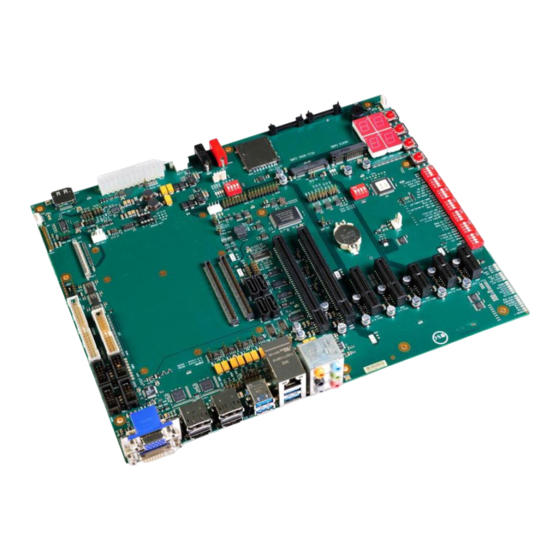
Page 11: Illustration 3 Picture
MSC C6-MB-EVA - PRELIMINARY - User Manual Illustration 3 Picture 11 / 63... -
Page 12: Mechanics
MSC C6-MB-EVA - PRELIMINARY - User Manual 3 Mechanics 3.1 Dimensions Dimension: 243.8 mm x 304.8 mm Width: 1.6 mm + /-10% Tolerances of the drill holes: +/- 0.1mm in X and Y Tolerances of the diameter: + 0.1 mm 3.2 Assembly notes... -
Page 13: Hardware
MSC C6-MB-EVA - PRELIMINARY - User Manual 4 Hardware 4.1 Plug-in Position of the COM Express module Socket for a COM Express type 6 module is available on the base board. Following form factors are supported: Mini Module ... - Page 14 MSC C6-MB-EVA - PRELIMINARY - User Manual Row A Row B GBE0_MDI3- GBE0_ACT# GBE0_MDI3+ LPC_FRAME# GBE0_LINK100# LPC_AD0 GBE0_LINK1000# LPC_AD1 GBE0_MDI2- LPC_AD2 GBE0_MDI2+ LPC_AD3 GBE0_LINK# LPC_DRQ0# GBE0_MDI1- LPC_DRQ1# GBE0_MDI1+ LPC_CLK GBE0_MDI0- PWRBTN# GBE0_MDI0+ SMB_CK GBE0_CTREF SMB_DAT SUS_S3# SMB_ALERT# SATA0_TX+ SATA1_TX+ SATA0_TX-...
-
Page 15: Table 1 Comexpress Connector Rows A And B
MSC C6-MB-EVA - PRELIMINARY - User Manual PCIE_TX4- PCIE_RX4- GPO2 PCIE_TX3+ PCIE_RX3+ PCIE_TX3- PCIE_RX3- PCIE_TX2+ PCIE_RX2+ PCIE_TX2- PCIE_RX2- GPI1 GPO3 PCIE_TX1+ PCIE_RX1+ PCIE_TX1- PCIE_RX1- WAKE0# GPI2 WAKE1# PCIE_TX0+ PCIE_RX0+ PCIE_TX0- PCIE_RX0- LVDS_A0+ LVDS_B0+ LVDS_A0- LVDS_B0- LVDS_A1+ LVDS_B1+ LVDS_A1- LVDS_B1- LVDS_A2+... - Page 16 MSC C6-MB-EVA - PRELIMINARY - User Manual Row C Row D USB_SSRX0- USB_SSTX0- USB_SSRX0+ USB_SSTX0+ USB_SSRX1- USB_SSTX1- USB_SSRX1+ USB_SSTX1+ USB_SSRX2- USB_SSTX2- USB_SSRX2+ USB_SSTX2+ USB_SSRX3- USB_SSTX3- USB_SSRX3+ USB_SSTX3+ DDI1_PAIR6+ DDI1_CTRLCLK_AUX+ DDI1_PAIR6- DDI1_CTRLDATA_AUX- RSVD RSVD RSVD RSVD PCIE_RX6+ PCIE_TX6+ PCIE_RX6- PCIE_TX6- PCIE_RX7+...
-
Page 17: Table 2 Comexpress Connector Rows C And D
MSC C6-MB-EVA - PRELIMINARY - User Manual PEG_RX1- PEG_TX1- TYPE1# TYPE2# PEG_RX2+ PEG_TX2+ PEG_RX2- PEG_TX2- PEG_RX3+ PEG_TX3+ PEG_RX3- PEG_TX3- RSVD RSVD RSVD RSVD PEG_RX4+ PEG_TX4+ PEG_RX4- PEG_TX4- RSVD PEG_RX5+ PEG_TX5+ PEG_RX5- PEG_TX5- PEG_RX6+ PEG_TX6+ PEG_RX6- PEG_TX6- PEG_RX7+ PEG_TX7+ PEG_RX7- PEG_TX7-... -
Page 18: Pci Express Lanes
MSC C6-MB-EVA - PRELIMINARY - User Manual 4.2 PCI Express Lanes 8 PCIe lanes are defined at the COM Express module. Some lanes can be routed to various connectors. Note: The number of PCIe lanes available will depend on the COM Express module used – not all modules can support 8 PCIe lanes. -
Page 19: Pci Express X4 Slots
MSC C6-MB-EVA - PRELIMINARY - User Manual 4.3 PCI Express x4 Slots Specification: References: X701, X702 Connector:FCI 10018784 Pin-out: Refer to PCI express specification PCIe slots are not hot-plug capable Signal Signal PRSNT1# JTAG_TCK SMB_CLK JTAG_TDI... -
Page 20: Table 5 Pin Out Pci Express
MSC C6-MB-EVA - PRELIMINARY - User Manual JTAG_TMS JTAG_RST# 3V3_AUX PE_RST# WAKE# RSVD REFCLK+ REFCLK- PET_p0 PET_n0 PER_p0 PER_n0 PRSNT2# RSVD PET_p1 PET_n1 PER_p1 PER_n1 PRSNT2# PET_p2 PET_n2 PER_p2 PER_n2 PET_p3 PET_n3 PER_p3 PER_n3 RSVD PRSNT2# RSVD Table 5 Pin out PCI Express... -
Page 21: Pci Express X1 Slots
MSC C6-MB-EVA - PRELIMINARY - User Manual 4.4 PCI Express x1 Slots Specification: X801 – X803 References: Connector:AMP / Tyco 4-1612163-1 Pin-out: Refer to PCI express specification PCIe slots are not hot-plug capable Signal Signal PRSNT1#... -
Page 22: Pci Express Mini Card
MSC C6-MB-EVA - PRELIMINARY - User Manual PE_RST# WAKE# RSVD REFCLK+ REFCLK- PET_p0 PET_n0 PER_p0 PER_n0 PRSNT2# Table 6 Pin out PCI Express 4.5 PCI Express Mini Card PCIe Lane 6 and the signals from USB port 6 switch automatic to this slot if a card is plugged. It can be selected with DIP switch 2 at S2901. -
Page 23: Pci Express X16 Graphics Slot
MSC C6-MB-EVA - PRELIMINARY - User Manual 4.6 PCI Express x16 Graphics Slot A PCIe x16 graphics slot is provided for insertion of PEG graphics cards. Specification: References: X501 Connector:AMP / Tyco 4-1612163-4 Pin-out: Refer to PCI express specification Pin D54 can be set to ground with PEG_LANE_RV# jumper J504. - Page 24 MSC C6-MB-EVA - PRELIMINARY - User Manual JTAG_TMS JTAG_RST# 3V3_AUX PE_RST# WAKE# RSVD REFCLK+ REFCLK- PET_p0 PET_n0 PER_p0 PER_n0 PRSNT2# RSVD PET_p1 PET_n1 PER_p1 PER_n1 PET_p2 PET_n2 PER_p2 PER_n2 PET_p3 PET_n3 PER_p3 PER_n3 RSVD PRSNT2# RSVD RSVD PET_p4 PET_n4 PER_p4...
-
Page 25: Table 7 Pin Out Pci Express X16 Graphics Slot
MSC C6-MB-EVA - PRELIMINARY - User Manual PET_n11 PER_p11 PER_n11 PET_p12 PET_n12 PER_p12 PER_n12 PET_p13 PET_n13 PER_p13 PER_n13 PET_p14 PET_n14 PER_p14 PER_n14 PET_p15 PET_n15 PER_p15 PER_n15 PRSNT2# (PEG_ENABLE#, D97 at X301) RSVD Table 7 Pin out PCI Express x16 Graphics Slot... -
Page 26: Add2 Card Slot
MSC C6-MB-EVA - PRELIMINARY - User Manual 4.7 ADD2 Card Slot The digital display interfaces can be switched to the ADD2-N (Advanced Digital Display - Normal) card slot. Refer to chapter 4.42. Specification: References: X601 Connector:AMP / Tyco 4-1612163-4 ... - Page 27 MSC C6-MB-EVA - PRELIMINARY - User Manual JTAG_TCK SMB_CLK JTAG_TDI SMB_DAT JTAG_TDO JTAG_TMS JTAG_RST# 3V3_AUX PE_RST# WAKE# RSVD REFCLK+ / n.c. REFCLK- / n.c. PET_p0 / DDI1 LANE0+ PET_n0 / DDI1 LANE0- PER_p0 / DDI1 LANE 5+ PER_n0 / DDI1 LANE 5-...
-
Page 28: Table 8 Pin Out Add2 Card Slot
MSC C6-MB-EVA - PRELIMINARY - User Manual PER_p10 / DDI3 AUX+ PER_n10 / DDI3 AUX- PET_p11 / DDI3 LANE3+ PET_n11 / DDI3 LANE3- PER_p11 / DDI3 HPD PER_n11 / DDI3 AUX SEL PET_p12 / n.c. PET_n12 / n.c. PER_p12 / n.c. -
Page 29: Vga Interface
MSC C6-MB-EVA - PRELIMINARY - User Manual 4.8 VGA Interface An analog display can be connected via a VGA (VESA DDC) interface. Specification: References: X1101 Pin-out: Refer to Table 8 Signal name Function Signal red GREEN Signal green... -
Page 30: Dvi-D Interface
MSC C6-MB-EVA - PRELIMINARY - User Manual BGND Ground blue +5V VDC SGND Ground Synchronisation Monitor ID Bit 0 (optional) DDC Data HSYNC Horizontal Sync. VSYNC Vertical Sync. DDC Clock Table 9 Pin-out VGA Interface DVI-D Interface Specification: References: X1101 ... -
Page 31: High Definition Multimedia Interface (Hdmi)
MSC C6-MB-EVA - PRELIMINARY - User Manual 4.10 High Definition Multimedia Interface (HDMI) Specification: References: X1201, X1301, X3401 Pin-out: Refer to Table 11 Signal name Function TMDS D2+ T.M.D.S. Data channel 2+ SHIELD 2 Shield connected to Ground TMDS D2- T.M.D.S. -
Page 32: Display Port (Dp)
MSC C6-MB-EVA - PRELIMINARY - User Manual TMDS D0- T.M.D.S. Data channel 0- TMDS CLK+ T.M.D.S. Clock channel + CLK SHIELD Clock Shield connected to Ground TMDS CLK- T.M.D.S. Clock channel - n.c. (consumer electronics control) reserved n.c. DDC CLK... -
Page 33: Embedded Display Port (Edp)
MSC C6-MB-EVA - PRELIMINARY - User Manual 4.12 Embedded Display Port (eDP) Specification: References: X1501 Connector:Tyco 5-2069716-3, I-PEX 20455-040E-02 Pin-out: Refer to Table 13 Signal name Function Reserved for LCD manufacturer’s use RSVD BL_PWR Backlight power BL_PWR... -
Page 34: Table 13 Pin-Out Embedded Display Port
MSC C6-MB-EVA - PRELIMINARY - User Manual SMBCLK RSVD System PWM signal input for dimming BL_PWM_DIM or NC (Optional) BL_ENABLE or NC Backlight On/0ff (Optional) BL_GND Backlight ground BL_GND Backlight ground BL_GND Backlight ground BL_GND Backlight ground Hot Plug Detect... -
Page 35: Alternative Embedded Display Port And Hdmi Connector
MSC C6-MB-EVA - PRELIMINARY - User Manual 4.13 Alternative Embedded Display Port and HDMI Connector The selection of these connectors is described in chapter 4.42 Specification: References: X3401 Pin-out: Refer to Table 12 and Table 13 Location: Refer to chapter 4.12 Embedded Display Port (eDP) -
Page 36: Lvds-Interface
MSC C6-MB-EVA - PRELIMINARY - User Manual 4.14 LVDS-Interface Any LCD display can be connected via a JILI30 connector. Two 24 bit LVDS channels are present on this 30-pin connector. The supply voltage of the display can be adjusted with jumper JP1701. The according position is printed on the PCB. -
Page 37: Lvds Eeprom Socket
MSC C6-MB-EVA - PRELIMINARY - User Manual Signal name Function LVDS_A0- LVDS Negative data signal (-) LVDS_A0+ LVDS Positive data signal (+) LVDS_A1- LVDS Negative data signal (-) LVDS_A1+ LVDS Positive data signal (+) LVDS_A2- LVDS Negative data signal (-) -
Page 38: Backlight Inverter Interface
MSC C6-MB-EVA - PRELIMINARY - User Manual Signal name Function EEPROM Address 0 (PD 10k) EEPROM Address 1 (PD 10k) EEPROM Address 2 (PD 10k) Ground Serial data Serial clock Write protection (Ground, disabled) Power supply 3V3 Table 16 Pin-out LVDS EEPROM Socket The LVDS EEPROM address can be select with the nearby jumper block JP1601. -
Page 39: Audio
MSC C6-MB-EVA - PRELIMINARY - User Manual 4.15 Audio A Realtek ALC888 HD audio codec is connected to the AC link of the COM Express module. Following LF signals are provided by the HDA codec: Stereo LineIn Stereo LineOut ... -
Page 40: Hda Connector
MSC C6-MB-EVA - PRELIMINARY - User Manual 4.15.1 HDA Connector Specification: References: X1801 Connector:Foxconn JAS331-H1G2-4F Pin-out: Refer to Table 19 Location: Refer to chapter 4.15 Audio Color Function light blue Line In lime Line Out pink... -
Page 41: Sata-Interface
MSC C6-MB-EVA - PRELIMINARY - User Manual 4.16 SATA-Interface Up to four SATA drives can be connected to the SATA interfaces. Note: Depending on the COM Express module used, not all SATA ports are available. For disk drive power there is one power supply connector available. -
Page 42: Msata Interface
MSC C6-MB-EVA - PRELIMINARY - User Manual Specification: References: X2101, X2102, X2103, X2104 Connector:FCI 10035691 Pin-out: Refer to Specification SATA [8, page 46, table 3] Specification Power Supply: References: X2105, X2106 Connector:AMP 171825-4 Pin-out: Refer to ATX specification V2.2 [2, "Floppy Drive Power Connector"]... -
Page 43: Usb Topology
MSC C6-MB-EVA - PRELIMINARY - User Manual 4.18 USB Topology Eight USB ports are normally provided by the COM Express module. The exact assignment of each port is defined in the following table: Location Power jumper Remarks USB-Port References Function... -
Page 44: Usb Power Supply
MSC C6-MB-EVA - PRELIMINARY - User Manual 4.18.1 USB Power Supply The power supplies are protected by USB power switches. With power jumper setting the USB power can be sourced from standard +5V (2-3) or from suspend +5V (1-2). The USB power switches have the following functions: ... -
Page 45: Usb Client Connector
MSC C6-MB-EVA - PRELIMINARY - User Manual 4.18.3 USB Client Connector The USB Port 7 signals were switched to a 5 pin header, if a USB client is plugged at X2003. The client control signal is routed to an auxiliary header X2705 at pin 2. -
Page 46: Table 28 Pin-Out Lpc-Slot
MSC C6-MB-EVA - PRELIMINARY - User Manual Signal Signal LPC_CLK LPC_FRAME# LPC_RST# VCC5V_SUS LPC_LAD3 LPC_LAD2 VCC3V3_SBY LPC_LAD1 LPC_LAD0 SMB_CLK SMB_DAT VCC3V3 SERIRQ PM_SUS_STAT# LPC_DRQ1# Table 28 Pin-out LPC-Slot 46 / 63... -
Page 47: Gpio
MSC C6-MB-EVA - PRELIMINARY - User Manual 4.21 GPIO The COM Express module provides four general purpose outputs and four general purpose inputs. The GPIs have pull-up resistors and are routed to a dip switch (S2907). With the dip switch the GPIs can be connected to ground. -
Page 48: Gpio Connector
MSC C6-MB-EVA - PRELIMINARY - User Manual 4.21.1 GPIO Connector Don’t set jumper J2801 to use the GPI signals at X2801. (Default) Specification: References: X2801 Connector:16 pin header, 2.54mm Pin-out: Refer to Table 29 Signal Signal GPI0... -
Page 49: Super Io
MSC C6-MB-EVA - PRELIMINARY - User Manual 4.23 Super IO The Winbond Super IO W83627HG is integrated on the base board. Interfaces used by the Super IO 2 RS232 interface (function of COM port shared with IrDA interface) ... -
Page 50: Sio Configuration
MSC C6-MB-EVA - PRELIMINARY - User Manual 4.23.1 SIO Configuration The SIO strap options can be changed via DIP switches S2902 and S2905. Switch Signal name Enable 24MHz S2902 #1 48MHz_EN Enable 48MHz (default) Reset FDC UARTs LPT No reset FDC UARTs... -
Page 51: Irda
MSC C6-MB-EVA - PRELIMINARY - User Manual Signal name Function DCD# Data Carrier Detect DSR# Data Set Ready Receive Data RTS# Request To Send Transmit Data CTS# Clear To Send DTR# Data Terminal Ready Ring Indicator Ground n. c. Table 33 Pin-out COM Ports 4.23.4... -
Page 52: Super Io Fan Interface
MSC C6-MB-EVA - PRELIMINARY - User Manual 4.23.6 Super IO Fan interface Two PWM controlled fan interfaces are integrated on the base board. Measurement of the tacho signal and control of the rotation speed is done by the Super IO. -
Page 53: Serial Smb Eeprom
MSC C6-MB-EVA - PRELIMINARY - User Manual 4.25 Serial SMB EEPROM For testing purposes a serial EEPROM (4kBit) is connected to the SMBus. To avoid address conflicts, the address can be selected with jumpers. Default resistor setting JP2503 Signal name... -
Page 54: Serial I2C-Bus Eeprom
MSC C6-MB-EVA - PRELIMINARY - User Manual 4.26 Serial I2C-Bus EEPROM For testing purposes two serial EEPROM (4kBit) are connected to the I2C bus. To avoid address conflicts, the address can be selected with jumpers. 4.26.1 Feature I2C EEPROM Default resistor setting... -
Page 55: Table 43 Pin-Out Lattice Programming Interface
MSC C6-MB-EVA - PRELIMINARY - User Manual Signal name Function Power Supply SDO_TDO Serial Data Out SDI_TDI Serial Data In ISPEN# Programming Enable Key-pin MODE_TMS Programming Mode Ground SCLK_TCK Serial Clock Table 43 Pin-out Lattice Programming Interface 55 / 63... -
Page 56: Feature Connector
MSC C6-MB-EVA - PRELIMINARY - User Manual 4.29 Feature Connector Many COMExpress signals are not used on this carrier. These signals and some other signals and power planes are available at the Feature connector. Specification Feature connector: References: X2701 ... -
Page 57: Power Supply Labor Connector
MSC C6-MB-EVA - PRELIMINARY - User Manual Signal name Function +12V VCC (inner pin 2.5mm diameter) Ground (shell 6.3mm diameter) Table 45 Pin-out Power IN3 connector 4.31 Power Supply Labor Connector The carrier can also be powered with +12VDC only. -
Page 58: Battery
MSC C6-MB-EVA - PRELIMINARY - User Manual 4.32 Battery The RTC on the COM Express module is buffered with a socketed battery on the base board. In order to clear the CMOS memory, the battery voltage to the COM Express module can be disconnected via nearby RTC BAT jumper J2701. -
Page 59: Leds
MSC C6-MB-EVA - PRELIMINARY - User Manual 4.38 LEDs There are many LEDs placed on the edge of the carrier. They indicate power and system states. Location: Refer to Illustration 4 Miscellaneous Parts Function Color Description WRONG T No type 6 module is plugged at X301. -
Page 60: Dip Switches
MSC C6-MB-EVA - PRELIMINARY - User Manual 4.40 DIP Switches There is an array of DIP switches at the card edge to configure various functions. References: S2901, S2902, S2903, S2904, S2905, S2906, S2908. Type: 4pol Location: Card edge Reference No. -
Page 61: Power Supply Current Measuring
MSC C6-MB-EVA - PRELIMINARY - User Manual 4.41.3 Power supply current measuring Since the sense resistors in the power supply lines of the COM Express module are removed in rev.3, the two jumpers J301 and J302 must be set for full ATX function. -
Page 62: Graphic Port Selection
MSC C6-MB-EVA - PRELIMINARY - User Manual 4.42 Graphic Port Selection Illustration 6 Block Diagram Graphics Ports 62 / 63... -
Page 63: Jili30 / Edp Selection
MSC C6-MB-EVA - PRELIMINARY - User Manual 4.42.1 JILI30 / eDP Selection Status DIP Switch No. Function S2905 JILI30 (LVDS) S2905 eDP (embedded Display Port 40pin) Table 48 JILI30 / eDP Selection 4.42.2 DDI Port Selection DP jumper Connector Source...
Need help?
Do you have a question about the COM Express MSC C6-MB-EVA and is the answer not in the manual?
Questions and answers