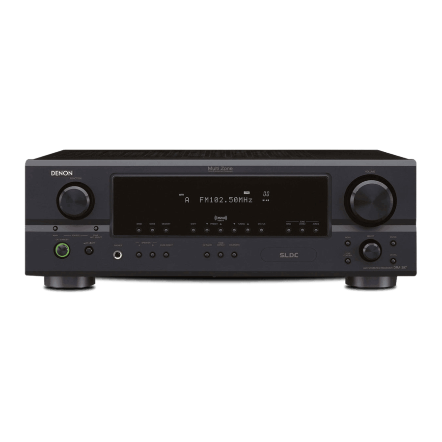
Denon DRA-397 Service Manual
Am-fm stereo receiver denon dra-397/ dra-297/ dra-37
Hide thumbs
Also See for DRA-397:
- Operating instructions manual (32 pages) ,
- Brochure & specs (2 pages) ,
- Operating instructions manual (39 pages)
Table of Contents
Advertisement
MODEL
For purposes of improvement, specifications and
design are subject to change without notice.
Please use this service manual with referring to the
operating instructions without fail.
Some illustrations using in this service manual are
slightly different from the actual set.
SERVICE MANUAL
DRA-397
DRA-297
DRA-37
AM-FM STEREO RECEIVER
TOKYO, JAPAN
Denon Brand Company, D&M Holdings Inc.
For U.S.A. & Canada model
Ver. 2
Please refer to the
MODIFICATION NOTICE.
X0282V.02 DE/CDM 0701
Advertisement
Table of Contents

Related Manuals for Denon DRA-397


Summary of Contents for Denon DRA-397
- Page 1 Please use this service manual with referring to the operating instructions without fail. Some illustrations using in this service manual are slightly different from the actual set. TOKYO, JAPAN Denon Brand Company, D&M Holdings Inc. X0282V.02 DE/CDM 0701...
-
Page 2: Safety Precautions
DRA-397/297/37 SAFETY PRECAUTIONS The following check should be performed for the continued protection of the customer and service technician. LEAKAGE CURRENT CHECK Before returning the unit to the customer, make sure you make either (1) a leakage current check or (2) a line to chassis resistance check. - Page 3 DRA-397/297/37 ADJUSTMENT Idling Current Required measurement equipment: DC Voltmeter 1. Preparation (1) Avoid direct blow from an air conditioner or an electric fan, and adjust the unit at normal room temperature 15 °C ~ 30 °C (59 °F ~ 86 °F).
- Page 4 DRA-397/297/37 BLOCK DIAGRAM DRA-397 model...
- Page 5 DRA-397/297/37 DRA-297/37 model...
- Page 6 DRA-397/297/37 LEVEL DIAGRAM...
- Page 7 DRA-397/297/37 SEMICONDUCTORS Only major semiconductors are shown, general semiconductors etc. are omitted to list. 1. IC’s M30624FGPFG (IC401) FRONT P.W.B.
- Page 8 DRA-397/297/37 M30624FGPFG Terminal Function PIN No. Port Function Port Name Function Standby P-ON SIRIUS_TX SIRIUS data transmission SIRIUS MUTE SIRIUS MUTE control (HD CE) HD Radio enable output MULT3 SW ZONE3 output, HPFcontrol HD Radio TX/(SDA) HD Radio data transmission...
- Page 9 DRA-397/297/37 PIN No. Port Function Port Name Function Standby P-ON HD Radio MUTE HD Radio MUTE control DC TRIGGER 1 Trigger Out1 ON/OFF control H/P RELAY H/P Relay control SW_MUTE SW MUTE control VIDEO OFF VIDEO Reg control HD Radio DET...
- Page 10 DRA-397/297/37 NJW1197 (IC101) INPUT P.W.B. PIN FUNCTION BLOCK DIAGRAM...
- Page 11 DRA-397/297/37 NJW1197 Terminal Function SYMBOL FUNCTION SYMBOL FUNCTION ROUT Rch output DCR_IN Multi-channel selector Rch input COUT Cch output DCR_OUT Input selector Rch output LSOUT LSch output Ground RSOUT RSch output DCL_IN Multi-channel selector Lch input LBOUT LBch output DCL_OUT...
- Page 12 DRA-397/297/37 F2602-1 XMDTIC (IC203) XM-READY P.W.B. Functionnal Description...
- Page 13 DRA-397/297/37 F2602-1 XMDTIC Pin Descriptions...
- Page 14 DRA-397/297/37 BA7626F (IC601) MAIN P.W.B. Block diagram Monitor OUT CTL A logic CTL E CTL B logic OUT2 CTL D CTL C Truth table Monitor OUT OUT1 OUT2 ∗ ∗ ∗ ∗ ∗ ∗ ∗ ∗ ∗ ∗ Note 1:...
- Page 15 DRA-397/297/37 AK4385 (IC 207) XM-READY P.W.B. MCLK DZFL BICK DZFR SDTI LRCK View AOUTL+ AOUTL- CCLK AOUTR+ CDTI AOUTR- Pin function Pin Name Function MCLK Master Clock Input Pin An external TTL clock should be input on this pin. BICK...
- Page 16 DRA-397/297/37 24LC16B (IC 404) FRONT P.W.B BLOCK DIAGRAM HV GENERATOR MEMORY EEPROM CONTROL CONTROL ARRAY XDEC LOGIC LOGIC PAGE LATCHES YDEC SENSE AMP R/W CONTROL CXA1511M (IC 201) XM-READY P.W.B. Block Diagram and Pin Configuration Head Limiter Delector & Hysteresis...
- Page 17 DRA-397/297/37 2. FL DISPLAY 16-ST-87GINK (FLT301) for DRA-397 model...
- Page 18 DRA-397/297/37...
- Page 19 DRA-397/297/37 HNA-16SM13T (FL301) for DRA-297, 37 model TUNED STEREO PHONO TUNER DVD / AUTO -2 -3 V.AUX TAPE ZONE2 PRO LOGIC DIGITAL DIGITAL ANALOG G2~G16 G12 G10 TUNED STEREO PHONO TUNER DVD / VDP TV / DBS AUTO -2 -3 V.AUX...
- Page 20 DRA-397/297/37 PRINTED WIRING BOARDS MAIN P.W.B. UNIT (for ALL model) COMPONENT SIDE...
- Page 21 DRA-397/297/37 FOIL SIDE...
- Page 22 DRA-397/297/37 FRONT P.W.B.UNIT (for DRA-397 model) DENON DENON DENON DENON COMPONENT SIDE...
- Page 23 DRA-397/297/37 FOIL SIDE...
- Page 24 DRA-397/297/37 FRONT P.W.B.UNIT (for DRA-297 model) DENON DENON DENON COMPONENT SIDE...
- Page 25 DRA-397/297/37 FOIL SIDE...
- Page 26 DRA-397/297/37 FRONT P.W.B.UNIT (for DRA-37 model) DENON DENON DENON COMPONENT SIDE...
- Page 27 DRA-397/297/37 FOIL SIDE...
- Page 28 DRA-397/297/37 INPUT P.W.B. UNIT (for ALL model) COMPONENT SIDE FOIL SIDE...
- Page 29 DRA-397/297/37 CNT P.W.B. UNIT (for ALL model) COMPONENT SIDE FOIL SIDE...
- Page 30 DRA-397/297/37 XM-READY P.W.B. UNIT (for ALL model) FUNCTUION SW P.W.B. UNIT (for DRA-37 model) DENON COMPONENT SIDE COMPONENT SIDE FOIL SIDE FOIL SIDE...
- Page 31 DRA-397/297/37 NOTE FOR PARTS LIST • Part indicated with the mark "nsp" are not always in stock and possibly to take a long period of time for supplying, or in some case supplying of part may be refused. • When ordering of part, clearly indicate "1" and "I" (i) to avoid mis- supplying.
- Page 32 DRA-397/297/37 PARTS LIST OF P.W.B. UNIT The parts listed below are for maintenance only, might differ from the parts used in the unit in appearances or dimensions. Part indicated with the mark “nsp” are not always in stock and possibly to take a long period of time for supplying, or in some case supplying of part may be refused.
- Page 33 DRA-397/297/37 Ref. No. Part No. Part Name Remarks Q'ty D522-525 00D 963 0058 407 D,SWITCHING IN4007 K000400700520S D526-532 00D 963 0020 309 D,SWITCHING 1SS133T K000013300520S D533 00D 960 0197 107 D,RECTIFIER KBPC604 6A K047604000020S D534-538 00D 963 0058 407 D,SWITCHING IN4007...
- Page 34 DRA-397/297/37 Ref. No. Part No. Part Name Remarks Q'ty R565-567 00D 960 9005 642 R,METAL FILM 1.2K-J,1W C060012265050S R576 00D 963 0310 501 R,METAL FILM 47K-J,1/4W C060047363050S R577,578 00D 963 0216 003 R,METAL FILM 0.22-J,1W C060R22065050S R584 00D 963 0310 404 R,METAL FILM 2.2K-J,1W...
- Page 35 DRA-397/297/37 Ref. No. Part No. Part Name Remarks Q'ty C537 00D 963 0312 703 C,ELECT 3300UF-M/35V D040332085050S C538 00D 963 0311 801 C,ELECT 1000UF-M/35V(SHL) D040102085040S C539,540 00D 963 0311 102 C,ELECT 1UF-M/50V (Pb Free) D040010087150S C541 00D 963 9003 097 C,FILM -0.1UF-K/250V...
- Page 36 DRA-397/297/37 Ref. No. Part No. Part Name Remarks Q'ty F501 00D 960 0005 804 HOLDER,FUSE CLIP G645000050010S F501B 00D 960 0005 804 HOLDER,FUSE CLIP G645000050010S F502 00D 960 0005 804 HOLDER,FUSE CLIP G645000050010S F502B 00D 960 0005 804 HOLDER,FUSE CLIP...
- Page 37 DRA-397/297/37 FRONT P.W.B. UNIT ASSY Ref. No. Part No. Part Name Remarks Q'ty SEMICONDUCTORS GROUP IC301 00D 960 0180 004 IC LC7572 for 297, 37 J127757210010S IC401 00D 963 0354 402 IC CPU MICRO PROCESS(L020) for 397 8952397000010 M30624FGPFP IC401...
- Page 38 DRA-397/297/37 Ref. No. Part No. Part Name Remarks Q'ty D404 00D 963 0020 309 D,SWITCHING 1SS133T K000013300520S D405 00D 963 0219 709 D,SWITCHING 1N4148W K005041480020S D407,408 00D 963 0219 709 D,SWITCHING 1N4148W K005041480020S D409 00D 963 0058 407 D,SWITCHING IN4007...
- Page 39 DRA-397/297/37 Ref. No. Part No. Part Name Remarks Q'ty C315 00D 963 0233 303 C,CERAMIC 0.01UF-M/16V for 397 D005103773530S C315 00D 963 9004 698 C,CERAMIC0.01UF-K/50V for 297, 37 D011103777160S C316 00D 963 0233 303 C,CERAMIC 0.01UF-M/16V for 397 D005103773530S C317 00D 963 9010 641 C,CERAMIC 0.047UF-K/16V...
- Page 40 DRA-397/297/37 Ref. No. Part No. Part Name Remarks Q'ty G301 RING,TER WIRE 120MM/1P 8410121010060S JACK104 00D 963 0146 209 TER,RCA 4PIN for 397 G602405B01000S JACK301 TER,RCA 2PIN for 37 G601207AE010YS JK301 00D 963 0294 708 JACK,D6.5 PHONE G402PJ612AG0YS L301 00D 960 0128 008 COIL,INDUCTOR 100UH...
- Page 41 DRA-397/297/37 INPUT P.W.B. UNIT ASS'Y Ref. No. Part No. Part Name Remarks Q'ty SEMICONDUCTORS GROUP IC101 00D 963 0295 202 IC NJW1197 J084119700010S IC104 00D 963 0202 305 IC NJM2068M J121206800020S IC105-107 00D 963 0202 305 IC NJM2068M for 397...
- Page 42 DRA-397/297/37 Ref. No. Part No. Part Name Remarks Q'ty C175-177 C,CERAMIC 0.1UF-K/50V D011104577161S C180 C,CERAMIC 0.1UF-K/50V for 397 D011104577161S C181 C,CERAMIC 0.1UF-K/50V D011104577161S C182-184 00D 963 0223 601 C,CERAMIC 100PF-J/50V D010101167160S C185,186 00D 963 0311 306 C,ELECT 10UF-M/50V D040100087070S C186FL...
- Page 43 DRA-397/297/37 XM-READY P.W.B. UNIT ASS'Y Ref. No. Part No. Part Name Remarks Q'ty SEMICONDUCTORS GROUP IC201 00D 960 0174 104 IC CXA1511M J030151100010S IC201 00D 263 1092 003 IC BA05T J126050000020S IC203 00D 262 3517 907 IC F2602 J080260200010S IC204...
- Page 44 DRA-397/297/37 Ref. No. Part No. Part Name Remarks Q'ty C237 00D 963 0224 105 C,CERAMIC 1000PF-K/50V D011102777160S C238 C,CERAMIC 0.1UF-K/50V D011104577161S C239 00D 963 0224 105 C,CERAMIC 1000PF-K/50V D011102777160S C240 C,CERAMIC 0.1UF-K/50V D011104577161S C241 00D 963 0311 607 C,ELECT 100UF-M/10V (Pb Free)
- Page 45 DRA-397/297/37 CTN P.W.B. UNIT ASS'Y Ref. No. Part No. Part Name Remarks Q'ty OTHERS PARTS GROUP CN407 00D 963 0097 303 CN.WAFER 2.0MM 15P L101100031510S CN409 00D 963 0097 303 CN.WAFER 2.0MM 15P L101100031510S CN506 00D 963 0097 303 CN.WAFER 2.0MM 15P...
- Page 46 DRA-397/297/37 EXPLODED VIEW DRA-397/297 model DRA397 BKE3 DRA397 BKE3 DRA397 BKE3 WARNING: Parts marked with this symbol have critical characteristics. Use ONLY replacement parts recommended by the manufacturer.
- Page 47 DRA-397/297/37 DRA-37 model WARNING: Parts marked with this symbol have critical characteristics. Use ONLY replacement parts recommended by the manufacturer.
- Page 48 00D 963 0304 300 PANEL FRONT for 297 3067212741100S 00D 963 0316 107 PANEL FRONT for 37 3067212731000S 00D 963 0051 501 BADGE DENON 5630210028000S 00D 963 0298 306 KNOB INPUT ASSY for 397 5088211278000SZ 00D 963 0138 301 KNOB INPUT...
- Page 49 DRA-397/297/37 Ref. No. Part No. Part Name Remarks Q'ty 00D 963 0094 801 BUTTON /3KEY(A) for 397, 297 5090211741000S 00D 963 0094 801 BUTTON /3KEY(A) for 37 5097211741000S 00D 963 0139 407 BUTTON 4KEY for 397, 297 5097212341000S 00D 963 0316 602 BUTTON 4KEY...
- Page 50 DRA-397/297/37 PACKING VIEW PARTS LIST OF PACKING & ACCESSORIES The parts listed below are for maintenance only, might differ from the parts used in the unit in appearances or dimensions. Part indicated with the mark “nsp” are not always in stock and possibly to take a long period of time for supplying, or in some case supplying of part may be refused.
- Page 51 DRA-397/297/37 WIRING DIAGRAM...
- Page 52 DRA-397/297/37...
- Page 53 DRA-397/297/37...
- Page 54 DRA-397/297/37 NOTE FOR SCHEMATIC DIAGRAM WARNING: Parts marked with this symbol ! have critical characteristics. Use ONLY replacement parts recommended by the manufactur- CAUTION: Before returning the unit to the customer, make sure you make µ either (1) a leakage current check or (2) a line to chassis resis- tance check.
- Page 55 DRA-397/297/37 SCHEMATIC DIAGRAMS (1/8) SIGNAL LINE SCHEMATIC DIAGRAMS (1/8) INPUT UNIT (for ALL model)
- Page 56 DRA-397/297/37 SCHEMATIC DIAGRAMS (2/8) SCHEMATIC DIAGRAMS (2/8) CPU/CNT UNIT (for ALL model)
- Page 57 DRA-397/297/37 SCHEMATIC DIAGRAMS (3/8) SIGNAL LINE SCHEMATIC DIAGRAMS (3/8) MAIN/POWER SW UNIT (for ALL model)
- Page 58 DRA-397/297/37 SCHEMATIC DIAGRAMS (4/8) SCHEMATIC DIAGRAMS (4/8) VIDEO UNIT FUNCTION SW UNIT (for ALL model)
- Page 59 DRA-397/297/37 SCHEMATIC DIAGRAMS (5/8) ZONE2 L ZONE2 R MUTE ZONE2 ZONE3 L ZONE3 R MUTE ZONE3 SCHEMATIC DIAGRAMS (5/8) FRONT/HEAD PHONE/ZONE UNIT (for DRA-397 model)
- Page 60 DRA-397/297/37 SCHEMATIC DIAGRAMS (6/8) SCHEMATIC DIAGRAMS (6/8) FRONT/HEAD PHONE/ZONE UNIT (for DRA-297 model)
- Page 61 DRA-397/297/37 SCHEMATIC DIAGRAMS (7/8) SCHEMATIC DIAGRAMS (7/8) FRONT/HEAD PHONE /FRONT PREOUT UNIT (for DRA-37 model)
- Page 62 DRA-397/297/37 SCHEMATIC DIAGRAMS (8/8) SCHEMATIC DIAGRAMS (8/8) XM READY UNIT (for ALL model)