Vertex Standard VX-800 Service Manual
Hide thumbs
Also See for VX-800:
- Operating manual (20 pages) ,
- Specifications (4 pages) ,
- Service manual (64 pages)
Table of Contents
Advertisement
Quick Links
VX-800
UHF Band
Service Manual
©2005 VERTEX STANDARD CO., LTD.
Operating Manual Reprint ................................................................................................................................................ 2
Set (Menu) Mode Functions .............................................................................................................................................. 8
Specification ....................................................................................................................................................................... 11
Exploded Views & Miscellaneous Parts ....................................................................................................................... 12
Block Diagram .................................................................................................................................................................... 13
Circuit Description ............................................................................................................................................................ 15
Alignment ........................................................................................................................................................................... 18
Board Units (Schematics, Layouts & Parts)
MAIN Unit ...................................................................................................................................................................... 25
VR Unit ............................................................................................................................................................................ 55
SW Unit ............................................................................................................................................................................ 56
Dummy Unit ................................................................................................................................................................... 57
Optional Board Units (Schematics, Layouts & Parts)
F2D-8 2-Tone Decode Unit ............................................................................................................................................ 58
VTP-50 VX-Trunk Unit .................................................................................................................................................. 60
FVP-25 Encryption / DTMF Pager Unit ...................................................................................................................... 62
F5D-14 5-Tone Unit ........................................................................................................................................................ 64
VERTEX STANDARD CO., LTD.
4-8-8 Nakameguro, Meguro-Ku, Tokyo 153-8644, Japan
VERTEX STANDARD
US Headquarters
10900 Walker Street, Cypress, CA 90630, U.S.A.
YAESU EUROPE B.V.
P.O. Box 75525, 1118 ZN Schiphol, The Netherlands
YAESU UK LTD.
Unit 12, Sun Valley Business Park, Winnall Close
Winchester, Hampshire, SO23 0LB, U.K.
VERTEX STANDARD HK LTD.
Unit 5, 20/F., Seaview Centre, 139-141 Hoi Bun Road,
Kwun Tong, Kowloon, Hong Kong
Introduction
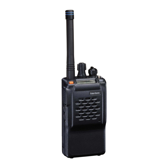
The Vertex Standard VX-800 is a compact, hand-held
portable transceiver for the UHF land mobile bands
that offers the convenience of small size, light
weight, and simple operation. The VX-800 can be
programmed by your Vertex Standard Dealer with
up to 200 channels for both single and split fre-
quency operation. The VX-800 provides up to 5 watts
of RF output power and includes a flexible quick-
connect antenna.
The transceiver and Ni-Cd, Li-Ion battery packs are
constructed of thick high impact polycarbonate plas-
tic, with special attention paid by the designers to
tight sealing and ruggedness, assuring years of reli-
able operation even in harsh environments.
The following pages describe the operation, features
and accessories of the VX-800. Following the dis-
cussion of transceiver operation, details regarding
programming software, alignment, and mainte-
nance will follow.
Contents
1
Advertisement
Table of Contents

Related Manuals for Vertex Standard VX-800


Summary of Contents for Vertex Standard VX-800
-
Page 1: Table Of Contents
The VX-800 can be programmed by your Vertex Standard Dealer with up to 200 channels for both single and split fre- quency operation. The VX-800 provides up to 5 watts of RF output power and includes a flexible quick- connect antenna. -
Page 2: Operating Manual Reprint
If you have a Speaker/Mi- crophone, we recommend that it not be connected un- til you are familiar with the basic operation of the VX-800. Operation Quick Start Turn the top panel’s VOL/PWR knob clock- To remove the battery, turn the radio off and re- move any protective cases. - Page 3 (when so programmed Soft Key and Toggle Switch Functions by your dealer) to start The VX-800 includes the [SEL1], [SEL2], [MON], and the scanner. The scanner rapidly steps through [LAMP] Keys, and the Toggle Switch, while the 16- each of the dealer-programmed channels, look- ing for incoming calls.
-
Page 4: Description Of Operating Functions
Operating Manual Reprint right, and their functions are explained on page 8. Soft Key Functions F o r f u r t h e r d e t a i l s , c o n t a c t y o u r None dealer. - Page 5 Operating Manual Reprint Note: Your dealer may have programmed your radio Note that your dealer may have made provision for to stay on one of the following channels if you “Talk Around” channels by programming “re- press the PTT switch during scanning pause: peater”...
- Page 6 Soft key. you change it. Channel Group Selection The VX-800 is capable of separating its 200 memory channels into any of ten Groups. There is no limit as to the number of channels which may be assigned...
- Page 7 Rapid Desktop Charger (for FNB-V57, FNB-V57IS, FNB-V62LI) Emergency NC-77B 120 VAC Compact Wall Charger for The VX-800 includes an “Emergency” feature which FNB-V57/-V57IS may be useful if you have someone monitoring on NC-77C 230-240 VAC Compact Wall Charger the same frequency as your transceiver’s channel.
-
Page 8: Set (Menu) Mode Functions
One or more of the radio’s "Soft Keys" may be en- abled for a function associated with the "Set" (Menu) The VX-800 has two scanning "list:" the "Dealer Scan" mode. This feature, when activated, allows the user list and the "User Scan" list. The "Dealer scan" list is... - Page 9 Set (Menu) Mode Functions No.11 ENCR (Encryption) After selecting this Menu, press the [SEL1] or [SEL2] key to select "P" (PTT Lock), "D" (Dial-Knob-Lock), On channels where scrambling is used, an incorrect "K" (Keypad Lock), or various combinations of these. setting of (or failure in) the encryption system at one Rotate the CH selector knob to save the new setting, end of the communication path will make it impos-...
- Page 10 Set (Menu) Mode Functions Note:...
-
Page 11: Specification
Specifications ENERAL Frequency Range: 400-430 MHz (Ver A), 440-470 MHz (Ver CS), 450-490 MHz (Ver D) Number of Channels: 200 channels Channel Spacing: 12.5/25 kHz Battery Voltage: 7.4 VDC Temperature Range: –22 °F to 140 °F (–30 °C to +60 °C) Frequency Stability: better than ±2.5 ppm Case Size (WHD):... -
Page 12: Exploded Views & Miscellaneous Parts
Exploded View & Miscellaneous Parts REF. VXSTD P/N Description Qty. U9900094 TAPTITE SCREW M2X5NI#2 U9900069 TAPTITE SCREW M2X9.5NI#2 U9900092 PAN HEAD SCREW M1.7X14AU#2 TAPTITE SCREW M1.7X5NI#2 (Lot. 1) U9900093 TAPTITE SCREW M1.7X4NI#2GUIDE (Lot. 2-) U9900084 BINDING HEAD SCREW M2X7.5B U9900063 TAPTITE SCREW 2X3.3NI U20305007 BINDING HEAD SCREW M3X5B RA0205600 (Lot. -
Page 13: Block Diagram
Block Diagram... - Page 14 Block Diagram Note:...
-
Page 15: Circuit Description
Circuit Description (44-11BF-P2, ±5.5 kHz BW) to strip away unwanted Overview mixer products. The VX-800U is a UHF/FM hand-held transceiver designed to operate in the frequency range of 400 to IF amplifier 512MHz. The first IF signal is amplified by Q1037 (2SC4215Y:Lot. - Page 16 Circuit Description The resulting DC squelch control voltage is passed If DTMF is enabled for transmission, the tone is gen- to pin 19 of the microprocessor Q1048. If no carrier erated by the microprocessor Q1048 and applied to is received, this signal causes pin 32 of Q1048 to go the splatter filter section in place of speech audio.
- Page 17 Circuit Description (UMC5N) and Q1018 to disable the supply voltage The output of the VCO is amplified by Q1041 and to the Power Module Q1019, thus disabling the trans- routed to the pin 5 of the PLL IC. The output of the mitter.
-
Page 18: Alignment
While Introduction most steps do not require all of the equipment listed, The VX-800 is carefully aligned at the factory for the the interactions of some adjustments may require specified performance across the frequency range that more complex adjustments be performed after- specified for each version. - Page 19 The alignment tool outline When connecting the CT-71 plug into the MIC/ Installation of the Alignment Tool SP jack of the VX-800, you must remove the This alignment tool consists of an executable file plastic cap and its mounting screws prior to “SVC31.exe”...
- Page 20 Alignment Alignment Sequence quency channel in the alignment range. Although the data displayed on the computer’s • Press the [space] key on the keyboard to acti- screen during alignment is temporary data, it is im- vate the transmitter. portant that you follow the basic alignment sequence •...
- Page 21 Alignment - [5] M • Press the [ ] or [ ] key, as needed, to set the AXIMUM EVIATION This section adjusts the transmitter’s voice devi- deviation to the desired value (typically 0.6±0.2 ation level. From the “(0) Common Tx” section, kHz, or 0.4±0.2 kHz for “narrow band”...
- Page 22 Alignment Channels deviation to the desired value (typically 3.9~4.2 The following parameters may be adjusted individu- kHz, or 2.0~2.3 kHz for "narrow band" channels). ally for each channel. For example, minor variations • When the desired deviation level is attained, in the power output across the operating band may press [ENTER] to lock in the new value.
- Page 23 N.C. Yellow (Pin 7: Clone) Note! Because of the bridge audio amplifier circuit used in the VX-800, it is necessry to construct and use a simple audio load test adapter as shown in the schematic diagram above, when conducting receiver alignment steps.
- Page 24 Note:...
-
Page 25: Main Unit
Main Unit (Lot. 1~3) 3.8V (0V) Circuit Diagram 2.7V (0V) +2 dBu 1.1V (0V) +16 dBu 4.7V (0V) -8 dBu +3 dBu 1.7V (0V) 1.2V (0V) 2.4V (0V) 0.6V (0V) -7 dBu Power 5W 3.0V 0V (5.0V) 2.8V (0V) 7.4V 0V (3.2V) 3.8V 0V (0.8V) - Page 26 Main Unit (Lot. 1~3) Note:...
- Page 27 Main Unit (Lot. 1~3) Parts Layout Side A TDA2822D TK71635SCL (L35) CPH6102 (AB) PDTC144EE (26) PDTC114TE (04) 2SA1774 (FR) DA221 (K) (Q1042) (Q1015, 1016, 1020, 1021, (Q1017,1063) (Q1008, 1044) (Q1026) (Q1062) (D1017, 1022,1027,1028, 1067) 1046,1059,1060) LC87F72C8A (Q1048) NJM2902V S-93C46AMFN S-80735SN-DZ (DZ) UMZ2N (Z2) XN1501 (5R) UMG2N (G2)
- Page 28 Main Unit (Lot. 1~3) Side B M68732HA-22 TA31136FN (Q1019) (Q1046) XP1501 (5R) CPH6102 (AB) UMC5N (C5) PDTC144EE (26) PDTC114TE 2SC4617 (BR) DA221 (K) BR715F (3D) (Q1003) (Q1064, 1065) (Q1035, 1036, 1040, 1055, (Q1006, 1031, 1032, (Q1038, 1051, 1053, 1061) (D1026, 1047, 1053, 1054) (D1019) (Q1002) 1056, 1066)
- Page 29 Main Unit (Lot. 4~50) Circuit Diagram...
- Page 30 Main Unit (Lot. 4~50) Note:...
- Page 31 Main Unit (Lot. 4~50) Parts Layout Side A TDA2822D TK71635SCL (L35) CPH6102 (AB) PDTC144EE (26) PDTC114TE (04) 2SA1774 (FR) DA221 (K) 2SC4617 (BR) (Q1042) (Q1015, 1016, 1020, 1021, (Q1017,1063) (Q1008, 1044) (Q1026) (Q1062) (D1017, 1022,1027,1028, (Q1049, 1050) 1067) 1046,1059,1060) LC87F72C8A (Q1048) NJM2902V S-93C46AMFN...
- Page 32 Main Unit (Lot. 4~50) Side B M68732HA-22 TA31136FN M68732LA-22 (Ver A;Lot. 6-) (Q1046) XP1501 (5R) CPH6102 (AB) UMC5N (C5) PDTC144EE (26) PDTC114TE 2SC4617 (BR) DA221 (K) BR715F (3D) (Q1019) (Q1003) (Q1064, 1065) (Q1035, 1040, 1055, 1056, (Q1006, 1031, 1032, 1058) (Q1038, 1051, 1053, 1061) (D1026, 1047, 1053, 1054) (D1019)
- Page 33 Main Unit (Lot. 51~) Circuit Diagram...
- Page 34 Main Unit (Lot. 51~) Note:...
- Page 35 Main Unit (Lot. 51~) Parts Layout Side A TDA2822D S-80735SN-DZ (DZ) TK71635SCL (L35) CPH6102 (AB) PDTC144EE (26) PDTC114TE (04) 2SA1774 (FR) DA221 (K) (Q1042; Lot. 1~52) (Q1015, 1016, 1020, 1021, (Q1017,1063) (Q1045; Lot. 1~30) (Q1008, 1044) (Q1026) (Q1062) (D1017, 1022,1027,1028, 1067) 1046,1059,1060) LC87F72C8A...
- Page 36 Main Unit (Lot. 51~) Side B M68732HA-22 TA31136FN M68732LA-22 (Ver A;Lot. 6~) (Q1046) TK71650SCL (L50) GN2011-Q (4W) XP1501 (5R) CPH6102 (AB) UMC5N (C5) PDTC114TE 2SC4617 (BR) DA221 (K) BR715F (3D) RA07M4452MSA-01 (Ver CS;Lot. 59~) (Q1005; Lot. 1~42) (D1030; Lot. 1~50) (Q1003) (Q1064, 1065) (Q1006, 1031, 1032, 1058)
-
Page 37: Parts List
Main Unit Parts List REF. DESCRIPTION VALUE TOL. MFR’S DESIG VS P/N VERS. LOT. SIDE LAY ADR *** MAIN UNIT *** PCB with Components (W/O LCD) CS1672001 VERSION D CS1672002 CS VERSION CS1672003 VERSION A Printed Circuit Board FR004420C FR004420D FR004420E C 1001 CHIP CAP. - Page 38 Main Unit REF. DESCRIPTION VALUE TOL. MFR’S DESIG VS P/N VERS. LOT. SIDE LAY ADR C 1025 CHIP TA.CAP. 10uF TEMSVB21C106M-8R K78120025 C 1026 CHIP CAP. 0.01uF GRM36B103K16PT K22128804 C 1027 CHIP CAP. 0.001uF GRM36B102K50PT K22178809 C 1029 CHIP CAP. 0.001uF GRM36B102K50PT K22178809...
- Page 39 Main Unit REF. DESCRIPTION VALUE TOL. MFR’S DESIG VS P/N VERS. LOT. SIDE LAY ADR C 1063 CHIP CAP. 0.1uF GRM36B104K10PT K22108802 C 1063 CHIP CAP. 0.01uF GRM36B103K16PT K22128804 C 1064 CHIP TA.CAP. 10uF TEMSVA1A106M-8R K78100028 C 1064 CHIP TA.CAP. 6.8uF TEMSVA1C685M-8R K78120056...
- Page 40 Main Unit REF. DESCRIPTION VALUE TOL. MFR’S DESIG VS P/N VERS. LOT. SIDE LAY ADR C 1106 CHIP CAP. 0.001uF GRM36B102K50PT K22178809 C 1107 CHIP CAP. 150pF GRM36CH151J50PT K22178240 C 1108 CHIP CAP. 150pF GRM36CH151J50PT K22178240 C 1109 CHIP CAP. 0.01uF GRM36B103K16PT K22128804...
- Page 41 Main Unit REF. DESCRIPTION VALUE TOL. MFR’S DESIG VS P/N VERS. LOT. SIDE LAY ADR C 1166 CHIP CAP. GRM36CH040C50PT K22178206 C 1166 CHIP CAP. GRM36CH040C50PT K22178206 CS VERSION 6- C 1166 CHIP CAP. GRM36CH050C50PT K22178207 VERSION A C 1166 CHIP CAP. GRM36CH040C50PT K22178206 VERSION D C 1167 CHIP CAP.
- Page 42 Main Unit REF. DESCRIPTION VALUE TOL. MFR’S DESIG VS P/N VERS. LOT. SIDE LAY ADR C 1214 CHIP CAP. 0.1uF GRM36B104K10PT K22108802 C 1215 CHIP CAP. GRM36CH050C50PT K22178207 C 1216 CHIP CAP. 0.1uF GRM36B104K10PT K22108802 C 1217 CHIP CAP. 0.1uF GRM36B104K10PT K22108802 C 1218 CHIP CAP.
- Page 43 Main Unit REF. DESCRIPTION VALUE TOL. MFR’S DESIG VS P/N VERS. LOT. SIDE LAY ADR C 1266 CHIP CAP. GRM36CH080D50PT K22178210 C 1267 CHIP CAP. 0.01uF GRM36B103K16PT K22128804 C 1268 CHIP CAP. 0.01uF GRM36B103K16PT K22128804 C 1269 CHIP CAP. 0.01uF GRM36B103K16PT K22128804 C 1270 CHIP CAP.
- Page 44 Main Unit REF. DESCRIPTION VALUE TOL. MFR’S DESIG VS P/N VERS. LOT. SIDE LAY ADR C 1320 CHIP CAP. 0.001uF GRM36B102K50PT K22178809 C 1321 CHIP CAP. 0.1uF GRM36B104K10PT K22108802 C 1322 CHIP CAP. GRM36CK020C50PT K22178204 C 1323 CHIP CAP. 0.001uF GRM39B102M50PT K22174809 C 1323 CHIP CAP.
- Page 45 Main Unit REF. DESCRIPTION VALUE TOL. MFR’S DESIG VS P/N VERS. LOT. SIDE LAY ADR D 1032 DIODE MA2S111-(TX) G2070614 D 1033 DIODE MA2S111-(TX) G2070614 D 1034 DIODE MA2S111-(TX) G2070614 D 1035 DIODE HVU350TRF G2070380 D 1036 DIODE HVC350B-TRF G2070596 D 1037 DIODE HVC350B-TRF G2070596...
- Page 46 Main Unit REF. DESCRIPTION VALUE TOL. MFR’S DESIG VS P/N VERS. LOT. SIDE LAY ADR L 1022 M.RFC LK1608 1R0K-T L1690687 L 1023 M.RFC LK1608 1R0K-T L1690687 L 1024 M.RFC 0.027uH HK1608 27NJ-T L1690521 L 1025 M.RFC 0.056uH HK1608 56NJ-T L1690525 L 1026 M.RFC...
- Page 47 1/16W 5% CR05-331J-H J24189271 R 1010 CHIP RES. 4.7k 1/16W 5% CR05-472J-H J24189285 R 1011 CHIP RES. 1/16W 5% CR05-473J-H J24189297 R 1012 CHIP RES. 1/16W 5% CR05-473J-H J24189297 R 1013 CHIP RES. 1/16W 5% CR05-220J-H J24189257 Please contact VERTEX STANDARD.
- Page 48 Main Unit REF. DESCRIPTION VALUE TOL. MFR’S DESIG VS P/N VERS. LOT. SIDE LAY ADR R 1014 CHIP RES. 1/16W 5% CR05-223J-H J24189293 R 1015 CHIP RES. 2.2k 1/16W 5% CR05-222J-H J24189281 R 1016 CHIP RES. 1.2k 1/16W 5% CR05-122J-H J24189278 R 1017 CHIP RES.
- Page 49 Main Unit REF. DESCRIPTION VALUE TOL. MFR’S DESIG VS P/N VERS. LOT. SIDE LAY ADR R 1067 CHIP RES. 1/16W 5% CR05-103J-H J24189289 R 1068 CHIP RES. 1/16W 5% CR05-103J-H J24189289 R 1069 CHIP RES. 1/16W 5% CR05-4R7J-H J24189249 R 1070 CHIP RES. 1/16W CR05-000-H J24189248...
- Page 50 Main Unit REF. DESCRIPTION VALUE TOL. MFR’S DESIG VS P/N VERS. LOT. SIDE LAY ADR R 1124 CHIP RES. 1/16W CR05-000-H J24189248 R 1125 CHIP RES. 1/16W 5% CR05-103J-H J24189289 R 1126 CHIP RES. 1/16W 5% CR05-103J-H J24189289 1-10 R 1126 CHIP RES. 6.8k 1/16W 5% CR05-682J-H...
- Page 51 Main Unit REF. DESCRIPTION VALUE TOL. MFR’S DESIG VS P/N VERS. LOT. SIDE LAY ADR R 1188 CHIP RES. 560k 1/16W 5% CR05-564J-H J24189310 R 1189 CHIP RES. 1/16W 5% CR05-102J-H J24189277 R 1190 CHIP RES. 1/16W 5% CR05-680J-H J24189263 R 1191 CHIP RES.
- Page 52 Main Unit REF. DESCRIPTION VALUE TOL. MFR’S DESIG VS P/N VERS. LOT. SIDE LAY ADR R 1246 CHIP RES. 1/16W 5% CR05-123J-H J24189290 R 1247 CHIP RES. 1.2k 1/16W 5% CR05-122J-H J24189278 R 1248 CHIP RES. 1/16W 5% CR05-683J-H J24189299 R 1249 CHIP RES.
- Page 53 Main Unit REF. DESCRIPTION VALUE TOL. MFR’S DESIG VS P/N VERS. LOT. SIDE LAY ADR R 1316 CHIP RES. 1/16W 5% CR05-102J-H J24189277 R 1317 CHIP RES. 1/16W 5% CR05-102J-H J24189277 R 1318 CHIP RES. 1/16W 5% CR05-102J-H J24189277 R 1319 CHIP RES. 1/16W 5% CR05-102J-H J24189277...
- Page 54 Main Unit REF. DESCRIPTION VALUE TOL. MFR’S DESIG VS P/N VERS. LOT. SIDE LAY ADR XF1002 XTAL FILTER MXF44.25-11B-FP2 H1102341 XF1002 XTAL FILTER HDF0028 44.25MHZ H1102338 MIC HOLDER RUBBER RA0207800 MIC HOLDER RUBBER RA0207900 MIC HOLDER RUBBER RA020790A SHIELD CASE VCO RA0208100 HOLDER PLATE (PM)
-
Page 55: Vr Unit
VR Unit Circuit Diagram Parts Layout Side A Side B BRPY1211F (D3002) Parts List REF. DESCRIPTION VALUE TOL. MFR’S DESIG VS P/N VERS. LOT. SIDE LAY ADR *** VR UNIT *** PCB with Components CB0971001 Printed Circuit Board FR004250D D 3001 LED LNJ808K8SRA G2070790 D 3002 LED... -
Page 56: Sw Unit
SW Unit Circuit Diagram Parts Layout Component Side Solder Side Parts List REF. DESCRIPTION VALUE TOL. MFR’S DESIG VS P/N VERS. LOT. SIDE LAY ADR *** SW UNIT *** PCB with Components CB0972001 Printed Circuit Board FR004410A S 3001 TACT SWITCH SOP-114HST R66-5374 N5090107 S 3002... -
Page 57: Dummy Unit
Dummy Unit Circuit Diagram Parts Layout Component Side Parts List REF. DESCRIPTION LOT. SIDE LAY ADR VALUE TOL. MFR’S DESIG VS P/N VERS. *** DUMMY UNIT *** PCB with Components CB0973001 Printed Circuit Board FR002510C C 4001 CHIP CAP. 0.0018uF GRM39B182M50PT K22174812 C 4002 CHIP CAP. -
Page 58: F2D-8 2-Tone Decode Unit
F2D-8 2-Tone Decode Unit Circuit Diagram Parts Layout Side A Side B TC7S04FU (E5) TA75S01F (SA) DTC124TU (05) HD64F3334YTF16 (Q1003) (Q1004) (Q1005) (Q1001) - Page 59 J24185104 R 1015 CHIP RES. 1/16W RMC1/16 183JATP J24185183 R 1016 CHIP RES. 1/16W RMC1/16 000JATP J24185000 R 1016 CHIP RES. 1/16W RMC1/16 273JATP J24185273 R 1017 CHIP RES. 1/16W RMC1/16 000JATP J24185000 BLIND SHEET RA0109300 Please contact VERTEX STANDARD.
-
Page 60: Vtp-50 Vx-Trunk Unit
VTP-50 VX-Trunk Unit Circuit Diagram Parts Layout Side B Side A BR93LC56FV NJM2904V MC68HSC705C8A502 TA75S01F (SA) (Q1004) (Q1001) (Q1002) (Q1003) - Page 61 VTP-50 VX-Trunk Unit Parts List REF. DESCRIPTION VALUE TOL. MFR’S DESIG VXSTD P/N VERS. LOT. SIDE LAY ADR *** VTP-50 *** Printed Circuit Board FR002540C C 1002 CHIP CAP. 0.001uF GRM39B102K50PT K22174821 C 1003 CHIP CAP. 0.01uF GRM39B103M25PT K22144802 C 1003 CHIP CAP. 0.01uF GRM39B103K25PT K22144803...
-
Page 62: Fvp-25 Encryption / Dtmf Pager Unit
FVP-25 Encryption / DTMF Pager Unit Circuit Diagram Parts Layout Side A Side B M64026FP LC73881 DTC144EU (26) (Q1001) (Q1002) (Q1003) - Page 63 FVP-25 Encryption / DTMF Pager Unit Parts List REF. DESCRIPTION VALUE TOL. MFR’S DESIG VXSTD P/N VERS. LOT. SIDE LAY ADR *** FVP-25 *** Printed Circuit Board FR005010F C 1001 CHIP CAP. 0.1uF GRM39B104K16PT K22124805 C 1002 CHIP CAP. 0.01uF GRM39B103M25PT K22144802 C 1003 CHIP CAP.
-
Page 64: F5D-14 5-Tone Unit
F5D-14 5-Tone Unit Circuit Diagram Parts Layout Side A Side B TK71650SC (L50) DTC114TE (04) PIC17LC44-08/PQ 2SC4617 (BR) MD09 BR93LC66FV (Q1001) (Q1002) (Q1003) (Q1004) (Q1005) (Q1006) - Page 65 F5D-14 5-Tone Unit Parts List REF. DESCRIPTION VALUE TOL. MFR’S DESIG VXSTD P/N VERS. LOT. SIDE LAY ADR *** F5D-14 *** Printed Circuit Board FR006510B Printed Circuit Board FR006510D C 1001 CHIP CAP. 0.1uF GRM36B104K10PT K22108802 C 1002 CHIP CAP. 0.0018uF GRM36B182K50PT K22178812...
- Page 66 Copyright 2005 VERTEX STANDARD CO., LTD. All rights reserved No portion of this manual may be reproduced without the permission of VERTEX STANDARD CO., LTD.
Need help?
Do you have a question about the VX-800 and is the answer not in the manual?
Questions and answers