Yamaha MG16/6FX Service Manual
Hide thumbs
Also See for MG16/6FX:
- Service manual (93 pages) ,
- Owner's manual (32 pages) ,
- Owner's manual (4 pages)
Table of Contents
Advertisement
A manufacture number should use this
manual with goods of 7 figures.
The example of a manufacture number.
LK01001
7 figures
The service manual of PA 011781 should
be used for the goods whose manufacture
number is 9 or more figures.
The example of a manufacture number.
JCLJ01001
UCCLJ01001
CHNCLJ01001
9-11 figures
011678
PA
200306-49800
CONTENTS
SPECIFICATIONS
CIRCUIT BOARD LAYOUT & WIRING
PA 011781
BLOCK DIAGRAM & LEVEL DIAGRAM
OVERALL CIRCUIT DIAGRAM
Copyright (c) Yamaha Corporation. All rights reserved. PDF-K6101
MIXING CONSOLE
SERVICE MANUAL
................................................ 3/5
............................................................ 7
..................................... 8
............................................ 12
.................................. 20
....................................... 21
....................................................... 29/35
PSR-A300
............................ 13
............................... 18
HAMAMATSU, JAPAN
'03.05
1
Advertisement
Table of Contents

Related Manuals for Yamaha MG16/6FX


Summary of Contents for Yamaha MG16/6FX
-
Page 1: Mixing Console
The example of a manufacture number. CIRCUIT BOARDS ........21 INSPECTIONS ............29/35 JCLJ01001 UCCLJ01001 PARTS LIST CHNCLJ01001 BLOCK DIAGRAM & LEVEL DIAGRAM 9-11 figures OVERALL CIRCUIT DIAGRAM 011678 HAMAMATSU, JAPAN 200306-49800 Copyright (c) Yamaha Corporation. All rights reserved. PDF-K6101 ’03.05... - Page 2 IMPOR TANT NOTICE This manual has been provided for the use of authorized Yamaha Retailers and their service personnel. It has been assumed that basic service procedures inherent to the industry, and more specifically Yamaha Products, are already known and under- stood by the users, and have therefore not been restated.
-
Page 3: Dimensions
MG16/6FX SPECIFICATIONS General Specifications Ω (with gain control at maximum level) Frequency Characteristics (ST OUT) 20 Hz–20 kHz +1 dB, –3 dB @+4 dBu, 600 Ω Total Harmonic Distortion (ST OUT) 0.1% (THD+N) @+14 dBu, 20 Hz–20 kHz, 600 (with gain control at maximum level) –128 dBu... - Page 4 MG16/6FX Input Specifications Input Appropriate Max. Before Connector Input Connector Gain Sensitivity* Rated Level Impedance Impedance Clipping Specifications –80 dBu –60 dBu –40 dBu –60 (0.078 mV) (0.775 mV) (7.75 mV) MIC INPUT Ω Ω 50–600 XLR-3-31 type (balanced) (CHs 1 to 8) –36 dBu...
- Page 5 MG16/6FX ST OUT GAIN 20 Hz 20 kHz +1 dB, –3 dB @+4 dBu , 600 ST OUT GAIN 0.1 % THD+N @+14 dBu, 20 Hz 20 kHz, 600 –128 dBu –100 dBu (ST OUT) ST OUT GROUP OUT –88 dBu 92 dB S/N &...
- Page 6 MG16/6FX MIC INPUT –80 dBu –60 dBu –40 dBu –60 (CH1 0.078 mV 0.775 mV 7.75 mV XLR-3-31 –36 dBu –16 dBu +4 dBu –16 12.3 mV 123 mV 1.23 V LINE INPUT –54 dBu –34 dBu –14 dBu 10 k –34...
- Page 7 MG16/6FX DIMENSIONS H 108 101.3 W 423 Units: mm...
-
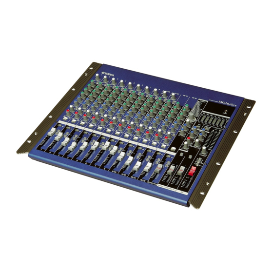
Page 8: Panel Layout
MG16/6FX PANEL LAYOUT Channel Control Section Channels Channels 1 to 8 9/10 to 15/16 (Monaural) (Stereo) [GAIN] Control [PEAK] Indicator [ 80 ] Switch (High Pass Filter) Equalizer ([HIGH], [MID], [LOW]) [AUX1] and [AUX2] Controls [PRE] Switch [EFFECT] Control [PAN] Control (CHs 1 to 8) - Page 9 MG16/6FX Master Control Section [ST] Master Fader [GROUP] Faders (1-2, 3-4) [TO ST] Switch Master SEND ([AUX1], [AUX2], and [EFFECT] controls) RETURN ([AUX1], [AUX2], and [ST] Controls) [2TR IN] Control [PHANTOM +48 V] Switch Level-Meter Signal Switches [C-R/PHONES] Control Level Meter...
- Page 10 MG16/6FX Rear Input/Output Section Channel Input Jacks [INSERT I/O] Jacks Channel Input Jacks [GROUP OUT] (1 to 4) Jacks [ST OUT] (L, R) Jacks [C-R OUT] Jacks [SEND] Jacks [RETURN] L (MONO), R Jacks [REC OUT] (L, R) Jacks [2TR IN] Jacks...
- Page 11 MG16/6FX Connector Polarities INPUT OUTPUT Pin 1: Ground MIC INPUT, ST OUT Pin 2: Hot (+) Pin 3: Cold (–) LINE INPUT (monaural channels), Tip: Hot (+) GROUP OUT, ST OUT, C-R OUT, Ring: Cold (–) AUX1, AUX2, EFFECT* Sleeve: Ground...
- Page 12 MG16/6FX CIRCUIT BOARD LAYOUT & WIRING MAIN MAIN MAIN Power switch and AC connector wiring Wiring to PS circuit board CN01 CN02 CN03 (PS circuit board) (PS circuit board) (PS circuit board) PS circuit board V9738100 (V975620) (V975600) Shrink tube (Seven places)
-
Page 13: Disassembly Procedure
MG16/6FX DISASSEMBLY PROCEDURE Rack Mount Angle (Time required: About 1 minute) Remove the two (2) screws marked [570A]. The rack mount angle R can then be removed. (Fig. 1) Remove the two (2) screws marked [570B]. The rack mount angle L can then be removed. (Fig. 1) - Page 14 MG16/6FX [A]: Bind Head Tapping Screw-B 3.0X8 MFZN2BL (EP600190) Photo.2 [530] [540] [530] [530]: Bind Head Tapping Screw-B 3.0X8 MFZN2BL (EP600190) [540]: Bind Head Tapping Screw-S 3.0X6 MFZN2BL (EP630210) IC02 IC03 Photo.1 [B]: Bind Head Tapping Screw-B 3.0X8 MFZN2BL (EP600190) Photo.3...
- Page 15 MG16/6FX [470A] [470B] [480A] [480B] [470A] [470B] [480B] [480A] [470A] [470B] [470]: Bind Head Tapping Screw-S [470]: Bind Head Tapping Screw-S 3.0X6 MFZN2BL (EP630210) 3.0X6 MFZN2BL (EP630210) [480]: Hexagonal Socket Set Screw [480]: Hexagonal Socket Set Screw 3.0X6 MFZN2BL (V9842300) 3.0X6 MFZN2BL (V9842300)
- Page 16 MG16/6FX MAIN (1/3, 2/3, 3/3) Circuit Boards (Time required: About 22 minutes) Remove the rack mount angle L and R. (See procedure 1.) Remove the bottom cover. (See procedure 2.) Remove the PS circuit board and Heat sink. (See procedure 3.) Remove the side cover L and R.
- Page 17 MG16/6FX 7-12 Remove the two (2) screws marked [430]. Twist the eight (8) hooks of the MIX1 support (upper) to become straight, and the support and two (2) spacer can be removed from the MAIN 1/3 circuit board. (Fig. 2, Photo. 10) 7-13 Remove the screw marked [440].
-
Page 18: Lsi Pin Description
MG16/6FX LSI PIN DESCRIPTION ZFX-2 (XY297A00) CPU DSP: ICM01 NAME FUNCTION NAME FUNCTION AXLR2 Audio Data Transmitt Unit 2/3 Left and Right Channel Frame Frequency Signal Audio Data Receive Unit 1 Data Input External Memory and I/O Data Bus Audio Data Receive Unit 2 Data Input... - Page 19 MG16/6FX µ PD78082 (XZ312A00) MCU DSP: ICM03 NAME FUNCTION NAME FUNCTION P12/ANI2 Non-connection P13/ANI3 P14/ANI4 Port 3 Port 1 / A/D converter analog input P15/ANI5 P16/ANI6 P35/PCL Port 3 / Clock output P17/ANI7 P36/BUZ Port 3 / Buzzer output P72/ASCK//SCK2...
-
Page 20: Ic Block Diagram
MG16/6FX IC BLOCK DIAGRAM NJM4580ED (XT157A00) 74HCU04DT (XZ110A00) NJM2068MD-T1 (XJ553A00) MAIN 1/3: IC102, 103, 202, 302, 303, 402, 502, MAIN 1/3: IC101, 201, 301, 401, 501, 601, 701, DSP: ICM05 503, 602, 702, 703, 802, 902-906, 801, 901, A01, F02, G02, J02, J03,... -
Page 21: Circuit Boards
MG16/6FX CIRCUIT BOARDS DSP Circuit Board (X3237A0)............21 MAIN 1/3 Circuit Board (X3235B0) .......... 22/24 MAIN 2/3 Circuit Board (X3235B0) .......... 26/27 MAIN 3/3 Circuit Board (X3235B0) ..........27 PS Circuit Board (X3232A0) ............28 Note: See parts list for details of circuit board component parts. - Page 22 MG16/6FX MAIN 1/3 Circuit Board to MAIN2/3-CN302 to MAIN2/3-CN702 to MAIN2/3-CN102 to MAIN2/3-CN502 to MAIN2 GAIN PEAK PEAK PEAK PEAK PEAK PEAK PEAK PEAK PEAK HIGH HIGH HI MID LO MID AUX1 AUX2 EFFECT PAN/BAL Fader 9/10...
- Page 23 MG16/6FX to MAIN2/3-CNA02 to MAIN2/3-CNF02 to PS-CN02 to MAIN2/3-CN902 to MAIN2/3-CND02 to MAIN2/3-CNK02 to PS-CN03 to MAIN3/3-CNL02 PEAK PEAK ST GRAPHIC EQUALIZER HIGH HIGH HIGH HIGH HI MID HI MID HI MID HI MID LO MID LO MID LO MID...
- Page 24 MG16/6FX MAIN 1/3 Circuit Board to DSP-CNM01...
- Page 25 MG16/6FX Pattern side...
- Page 26 MG16/6FX MAIN 2/3 Circuit Board LINE INSERT I/O to MAIN1/3-CN101 to MAIN1/3-CN301 to MAIN1/3-CN501 to MAIN1/3-CN701 GROUP OUT ST OUT 14/R 16/R 9/10 11/12 2TR IN 13/L 15/L C-R OUT 10/R 12/R 14/R 16/R AUX2 SEND RETURN 11/L 13/L 15/L...
- Page 27 MG16/6FX MAIN 2/3 Circuit Board Pattern side MAIN 3/3 Circuit Board to MAIN 1/3-CNL01 PHONES Pattern side Component side...
-
Page 28: Power Switch
MG16/6FX PS Circuit Board to Power Switch, AC connector to MAIN 1/3 -CNJ01 to MAIN 1/3 -CNE02 Component side Pattern side... - Page 29 MG16/6FX INSPECTIONS Scope This inspection specifications is applied to the mixer MG16/6FX. Power Supply AC Adaptor shall be used. V981110(H:230V 50Hz) or V981090(U:120V 60Hz), V981240(B:230V 50Hz), V981700(K:220V 60Hz), V986250(A:240V 50Hz) Power Indicator Inspection POWER LED shall light when the unit is turned on.
- Page 30 MG16/6FX •ST CH (13/14,15/16) EQ(HIGH,HI-MID,LO-MID,LOW) level control CENTER AUX1,AUX2 level control AUX2 PRE switch OFF(POST) EFFECT level control PAN/BAL control L(turned counterclockwise fully) ON switch ON(LED shall light) when taking measurement only/ OFF otherwise PFL switch ON(LED shall light) when taking measurement only/ OFF otherwise...
- Page 31 MG16/6FX Table 4.2-2 [dBu] INPUT INPUT level GAIN INSERT OUT REC OUT L REC OUT R -20 ± 2 – – +2.2 ± 2 +2.2 ± 2 CH1 INSERT IN Unspecified – +2.2 ± 2 CH2-8 INSERT IN Unspecified –...
- Page 32 MG16/6FX 4.5 Channel Equalizer Characteristics In the state checked in 4.1 above, check the output level obtained at GROUP 1 OUT in the case of CH INPUT and ST CH INPUT L and at GROUP 2 OUT in the case of ST CH INPUT R when LO, HI and MID of INPUT are moved respectively.
- Page 33 MG16/6FX 4.8 PEAK LED light-up level In the state 4.1, each LED shall light-up when a signal specified as below is fed to the MIC input. Table 4.8-1 [dBu] INPUT PEAK LED -43 ± 2 4.9 Meter LED lighting check PEAK LED lights up, when ST output level reaches +17.5 ±...
- Page 34 MG16/6FX 4.16 DIGITAL EFFECT Set the CH1 as follows and feed -40dBu signal to CH1 MIC. GAIN VR,AUX1 VR,AUX2 VR: Fader,EFFECT VR: ON,PFL,1-2,3-4 switch: When setting EFFECT RTN fader and VR to MAX and each switch(ON,PFL,1-2,3-4) to ON,the output level shall be within the range specified the Table 4.16-1.
- Page 35 MG16/6FX...
- Page 36 MG16/6FX INPUT AUX2 C-R OUT C-R OUT INPUT Gain ST L OUT ST R OUT GROUP1-4 AUX1 EFFECT level PRE OFF PRE ON +1 ± 2 *1 +1 ± 2 *1 +4 ± 2 -4 ± 2 +6 ± 2 -4 ±...
- Page 37 MG16/6FX INPUT INPUT level GAIN INSERT OUT REC OUT L REC OUT R -20 ± 2 – – +2.2 ± 2 +2.2 ± 2 CH1 INSERT IN Unspecified – +2.2 ± 2 CH2-8 INSERT IN Unspecified – – INPUT AUX2...
- Page 38 MG16/6FX Level control f control Applied frequency Variation width +12 ± 2 – HIGH 10kHz -12 ± 2 – +15 ± 2.5 5kHz -15 ± 2.5 +15 ± 2.5 250Hz -15 ± 2.5 +12 ± 2 – 100Hz -12 ± 2 –...
- Page 39 MG16/6FX INPUT PEAK LED -43 ± 2 Fader/VR ST OUT GROUP OUT AUX OUT EFFECT OUT C-R OUT -100 -100 -100 -100...
- Page 40 MG16/6FX OUTPUT PROGRAM select switch PARAMETER OUTPUT level ST L OUT +4.5 ± 3 ST R OUT GROUP1-4 9: VOCAL ECHO 1 AUX1,2 +0.5 ± 3 C-R OUT L C-R OUT R ST L OUT 1: HALL1~16: VOCAL REVERB -6 ± 25...
-
Page 41: Parts List
MIXING CONSOLE PARTS LIST CONTENTS OVERALL ASSEMBLY ..........2 ELECTRICAL PARTS ........4-38 Notes : DESTINATION ABBREVIATIONS A : Australian model M : South African model B : British model O : Chinese model C : Canadian model Q : South-east Asia model D : German model T : Taiwan model E : European model... - Page 42 MG16/6FX OVERALL ASSEMBLY MAIN 2/3 MAIN 3/3 MAIN 1/3 AC Adaptor (U) OUTPUT : AC18V X 2 1.4A (2) GND (3) AC (1) AC...
- Page 43 MG16/6FX PART NO. DESCRIPTION REMARKS REF NO. RANK OVERALL ASSEMBLY MG16/6FX (V981900) V 9 7 3 7 6 0 0 Circuit Board MAIN (1/3,2/3,3/3) V 9 7 3 8 1 0 0 Circuit Board V 9 7 3 8 2 0 0...
- Page 44 MG16/6FX ELECTRICAL PARTS PART NO. DESCRIPTION REMARKS REF NO. RANK ELECTRICAL PARTS MG16/6FX V 9 7 3 8 2 0 0 Circuit Board (X3237A0) V 9 7 3 7 6 0 0 Circuit Board MAIN (1/3,2/3,3/3) (X3235B0) V 9 7 3 8 1 0 0...
- Page 45 MG16/6FX PART NO. DESCRIPTION REMARKS REF NO. RANK RM13 VV313600 Flame Proof C. Resistor 2.2 1/4 J RM14 V 9 7 1 4 8 0 0 Carbon Resistor (chip) 22K 0.1 J V 9 7 1 4 8 0 0 Carbon Resistor (chip) 22K 0.1 J...
- Page 46 MG16/6FX PART NO. DESCRIPTION REMARKS REF NO. RANK C138 V 9 7 2 6 6 0 0 Electrolytic Cap. 47.00 25.0V C139 V 9 7 2 2 7 0 0 Ceramic Capacitor (chip) 0.01 50V M 0603 C140 V 9 7 2 2 7 0 0 Ceramic Capacitor (chip) 0.01 50V M 0603...
- Page 47 MG16/6FX PART NO. DESCRIPTION REMARKS REF NO. RANK C320 VV190000 Mylar Capacitor 820P 50V J C321 V 9 7 2 0 9 0 0 Ceramic Capacitor (chip) 33P 50V K 0603 C322 V 9 7 2 1 5 0 0...
- Page 48 MG16/6FX PART NO. DESCRIPTION REMARKS REF NO. RANK C506 V 9 7 2 0 9 0 0 Ceramic Capacitor (chip) 33P 50V K 0603 C507 V 9 7 2 1 5 0 0 Ceramic Capacitor (chip) 100P 50V K 0603...
- Page 49 MG16/6FX PART NO. DESCRIPTION REMARKS REF NO. RANK C635 V 9 7 2 6 5 0 0 Electrolytic Cap. 10.00 25.0V C636 V 9 7 2 1 5 0 0 Ceramic Capacitor (chip) 100P 50V K 0603 C637 V 9 7 2 1 3 0 0...
- Page 50 MG16/6FX PART NO. DESCRIPTION REMARKS REF NO. RANK C818 V 9 7 2 6 5 0 0 Electrolytic Cap. 10.00 25.0V C819 VV062300 Mylar Capacitor 0.039 50V J C820 VV190000 Mylar Capacitor 820P 50V J C821 V 9 7 2 0 9 0 0...
- Page 51 MG16/6FX PART NO. DESCRIPTION REMARKS REF NO. RANK C949 V 9 7 2 0 7 0 0 Ceramic Capacitor (chip) 22P 50V K 0603 C950 V 9 7 2 0 7 0 0 Ceramic Capacitor (chip) 22P 50V K 0603...
- Page 52 MG16/6FX PART NO. DESCRIPTION REMARKS REF NO. RANK CA44 VV060600 Mylar Capacitor 3300P 50V J CA45 V 9 7 2 1 5 0 0 Ceramic Capacitor (chip) 100P 50V K 0603 CA46 VV061300 Mylar Capacitor 8200P 50V J CA47 V 9 7 2 1 5 0 0...
- Page 53 MG16/6FX PART NO. DESCRIPTION REMARKS REF NO. RANK CB37 VV061300 Mylar Capacitor 8200P 50V J CB38 VV060600 Mylar Capacitor 3300P 50V J CB39 V 9 7 2 1 5 0 0 Ceramic Capacitor (chip) 100P 50V K 0603 CB40 V 9 7 2 1 5 0 0...
- Page 54 MG16/6FX PART NO. DESCRIPTION REMARKS REF NO. RANK CC50 V 9 7 2 1 3 0 0 Ceramic Capacitor (chip) 68P 50V K 0603 CC51 V 9 7 2 1 3 0 0 Ceramic Capacitor (chip) 68P 50V K 0603...
- Page 55 MG16/6FX PART NO. DESCRIPTION REMARKS REF NO. RANK CG14 V 9 7 2 1 3 0 0 Ceramic Capacitor (chip) 68P 50V K 0603 CG15 V 9 7 2 6 7 0 0 Electrolytic Cap. 100.00 25.0V CG16 V 9 7 2 6 7 0 0 Electrolytic Cap.
- Page 56 MG16/6FX PART NO. DESCRIPTION REMARKS REF NO. RANK CK45 VV060900 Mylar Capacitor 4700P 50V J CK46 VV060300 Mylar Capacitor 2200P 50V J CK47 VV060000 Mylar Capacitor 1200P 50V J CK48 V 9 7 2 1 8 0 0 Ceramic Capacitor (chip)
- Page 57 MG16/6FX PART NO. DESCRIPTION REMARKS REF NO. RANK V 9 7 2 2 7 0 0 Ceramic Capacitor (chip) 0.01 50V M 0603 CN101 WA594800 Cable Holder TB2062 13P TE CN102 WA594800 Cable Holder TB2062 13P TE CN301 WA594800 Cable Holder...
- Page 58 MG16/6FX PART NO. DESCRIPTION REMARKS REF NO. RANK ICG01 XJ553A00 NJM2068MD-T1 OP AMP ICG02 XT157A00 NJM4580ED OP AMP ICG03 XJ553A00 NJM2068MD-T1 OP AMP ICJ01 XJ553A00 NJM2068MD-T1 OP AMP ICJ02 XT157A00 NJM4580ED OP AMP ICJ03 XT157A00 NJM4580ED OP AMP ICK01 XJ553A00...
- Page 59 MG16/6FX PART NO. DESCRIPTION REMARKS REF NO. RANK LD101 V 9 7 9 0 4 0 0 LED Red HFR203PJ-3-00 PEAK 1 LD102 V 9 8 5 4 5 0 0 LED Yellow HFY803037TP-50-00 PFL 1 LD103 V 9 8 5 4 5 0 0...
- Page 60 MG16/6FX PART NO. DESCRIPTION REMARKS REF NO. RANK Q202 VV556400 Transistor 2SC2412K Q,R,S Q203 V 7 4 2 1 7 0 0 Transistor 2SC3324 GR,BL Q204 VV556400 Transistor 2SC2412K Q,R,S Q205 VV556400 Transistor 2SC2412K Q,R,S Q206 VV556500 Transistor 2SA1037AK Q,R,S...
- Page 61 MG16/6FX PART NO. DESCRIPTION REMARKS REF NO. RANK R103 V 9 7 1 9 3 0 0 Metal Film Resistor (chip) 47K 1/16 D R104 V 9 7 1 9 3 0 0 Metal Film Resistor (chip) 47K 1/16 D...
- Page 62 MG16/6FX PART NO. DESCRIPTION REMARKS REF NO. RANK R214 V 9 7 1 9 0 0 0 Metal Film Resistor (chip) 33K 1/16 D R215 V 9 7 1 9 0 0 0 Metal Film Resistor (chip) 33K 1/16 D...
- Page 63 MG16/6FX PART NO. DESCRIPTION REMARKS REF NO. RANK R328 V 9 7 1 3 3 0 0 Carbon Resistor (chip) 4.7K 0.1 J R329 V 9 7 1 3 8 0 0 Carbon Resistor (chip) 8.2K 0.1 J R330 V 9 7 1 3 3 0 0 Carbon Resistor (chip) 4.7K 0.1 J...
- Page 64 MG16/6FX PART NO. DESCRIPTION REMARKS REF NO. RANK R444 V 9 7 1 4 4 0 0 Carbon Resistor (chip) 15K 0.1 J R445 V 9 7 0 9 9 0 0 Carbon Resistor (chip) 10 0.1 J R446 V 9 7 1 4 6 0 0 Carbon Resistor (chip) 18K 0.1 J...
- Page 65 MG16/6FX PART NO. DESCRIPTION REMARKS REF NO. RANK R557 V 9 7 1 1 3 0 0 Carbon Resistor (chip) 220 0.1 J R571 V 9 7 1 1 5 0 0 Carbon Resistor (chip) 330 0.1 J R572 V 9 8 4 4 9 0 0 Metal Film Resistor 6.8K 1/4 F...
- Page 66 MG16/6FX PART NO. DESCRIPTION REMARKS REF NO. RANK R704 V 9 7 1 9 3 0 0 Metal Film Resistor (chip) 47K 1/16 D R705 V 9 7 0 9 9 0 0 Carbon Resistor (chip) 10 0.1 J R706...
- Page 67 MG16/6FX PART NO. DESCRIPTION REMARKS REF NO. RANK R818 V 9 7 1 5 2 0 0 Carbon Resistor (chip) 33K 0.1 J R819 V 9 7 0 9 9 0 0 Carbon Resistor (chip) 10 0.1 J R820 V 9 7 1 6 6 0 0 Carbon Resistor (chip) 220K 0.1 J...
- Page 68 MG16/6FX PART NO. DESCRIPTION REMARKS REF NO. RANK R924 V 9 7 1 3 3 0 0 Carbon Resistor (chip) 4.7K 0.1 J R925 V 9 7 1 4 0 0 0 Carbon Resistor (chip) 10K 0.1 J R926 V 9 7 1 3 3 0 0 Carbon Resistor (chip) 4.7K 0.1 J...
- Page 69 MG16/6FX PART NO. DESCRIPTION REMARKS REF NO. RANK RA07 WB082500 Metal Film Resistor (chip) 360 .06 D RA08 V 9 7 1 8 5 0 0 Metal Film Resistor (chip) 10K 1/16 D RA09 V 9 7 1 8 5 0 0...
- Page 70 MG16/6FX PART NO. DESCRIPTION REMARKS REF NO. RANK RA85 V 9 7 1 1 3 0 0 Carbon Resistor (chip) 220 0.1 J RA86 V 9 7 1 1 3 0 0 Carbon Resistor (chip) 220 0.1 J RA91 V 9 8 4 4 9 0 0 Metal Film Resistor 6.8K 1/4 F...
- Page 71 MG16/6FX PART NO. DESCRIPTION REMARKS REF NO. RANK RC12 V 9 7 1 3 3 0 0 Carbon Resistor (chip) 4.7K 0.1 J RC13 V 9 7 1 4 0 0 0 Carbon Resistor (chip) 10K 0.1 J RC14 V 9 7 1 3 3 0 0 Carbon Resistor (chip) 4.7K 0.1 J...
- Page 72 MG16/6FX PART NO. DESCRIPTION REMARKS REF NO. RANK RE04 V 9 7 1 6 6 0 0 Carbon Resistor (chip) 220K 0.1 J RE05 V 9 7 1 3 3 0 0 Carbon Resistor (chip) 4.7K 0.1 J V 9 7 1 3 3 0 0 Carbon Resistor (chip) 4.7K 0.1 J...
- Page 73 MG16/6FX PART NO. DESCRIPTION REMARKS REF NO. RANK V 9 7 1 6 1 0 0 Carbon Resistor (chip) 75K 0.1 J RJ04 V 9 7 1 1 3 0 0 Carbon Resistor (chip) 220 0.1 J V 9 7 1 1 3 0 0 Carbon Resistor (chip) 220 0.1 J...
- Page 74 MG16/6FX PART NO. DESCRIPTION REMARKS REF NO. RANK RL06 V 9 7 1 6 3 0 0 Carbon Resistor (chip) 100K 0.1 J RL08 V 9 7 3 3 2 0 0 Carbon Resistor 1.5K 1/8 J RL09 V 9 7 1 5 2 0 0 Carbon Resistor (chip) 33K 0.1 J...
- Page 75 MG16/6FX PART NO. DESCRIPTION REMARKS REF NO. RANK SW401 V 9 6 8 3 6 0 0 Push Switch PS-22E85L HPF 4 SW402 V 9 6 8 3 6 0 0 Push Switch PS-22E85L PFL 4 SW403 V 9 6 8 3 6 0 0...
- Page 76 MG16/6FX PART NO. DESCRIPTION REMARKS REF NO. RANK VR109 V 9 7 9 1 0 0 0 Rotary Variable Resistor B 20.0K XV09213Y AUX2 1 VR110 V 9 7 9 1 0 0 0 Rotary Variable Resistor B 20.0K XV09213Y...
- Page 77 MG16/6FX PART NO. DESCRIPTION REMARKS REF NO. RANK VR809 V 9 7 9 1 0 0 0 Rotary Variable Resistor B 20.0K XV09213Y AUX2 8 VR810 V 9 7 9 1 0 0 0 Rotary Variable Resistor B 20.0K XV09213Y...
- Page 78 MG16/6FX PART NO. DESCRIPTION REMARKS REF NO. RANK V 9 7 2 5 1 0 0 Ceramic Capacitor 4700P 500V Z ST V 9 7 2 5 1 0 0 Ceramic Capacitor 4700P 500V Z ST V 9 7 2 7 0 0 0 Electrolytic Cap.
-
Page 79: Circuit Diagram
MIXING CONSOLE MG16/6FX CIRCUIT DIAGRAM CONTENTS BLOCK DIAGRAM ....3 OVERALL CIRCUIT DIAGRAM MAIN 1/3 ..............4-10 MAIN 2/3 ..............11, 12 MAIN 3/3 ................. 8 DSP ................13 PS ................... 14 Notation for Circuit Diagrams 1. How to identify inter-sheet connectors... - Page 80 BLOCK DIAGRAM & LEVEL DIAGRAM MG16/6FX MAIN2/3 JK101, 201, 301, CH IN MAIN1/3 +48V 401, 501, 601, CH1-8 701, 801 PHANTOM GROUP OUT [-60dBu to -16dBu] IC101, 201, 301, 401, IC103, 303, IC102, 202, 302, 402, ICF01a (8P) ICF02b (8P)
- Page 81 OVERALL CIRCUIT DIAGRAM 1/11 (MAIN1/3) MG16/6FX MAIN1/3 OP AMP to Page 8: P2 to Page 6: P9 OP AMP to Page 8: P3 OP AMP OP AMP to Page 9: K8 OP AMP to Page 9: J8 to Page 9: H8...
- Page 82 OVERALL CIRCUIT DIAGRAM 2/11 (MAIN1/3) MG16/6FX OP AMP MAIN1/3 to Page 8: P2 OP AMP to Page 8: P3 OP AMP OP AMP OP AMP to Page 9: K8 to Page 9: J8 to Page 9: H8 to Page 9: G8...
- Page 83 OVERALL CIRCUIT DIAGRAM 3/11 (MAIN1/3) MG16/6FX MAIN1/3 to Page 8: P2 OP AMP to Page 8: P3 OP AMP OP AMP OP AMP to Page 9: K8 OP AMP to Page 9: J8 CH9/10 OP AMP to Page 9: H8...
- Page 84 OVERALL CIRCUIT DIAGRAM 4/11 (MAIN1/3) MG16/6FX from Page 6: C11 from Page 6: B11 MAIN1/3 OP AMP OP AMP to Page 8: P2 CH13/14 to Page 8: P3 OP AMP OP AMP OP AMP to Page 9: K8 OP AMP...
- Page 85 OVERALL CIRCUIT DIAGRAM 5/11 (MAIN1/3, MAIN3/3) MG16/6FX MAIN1/3 OP AMP OP AMP from Page 4: A1, Page 5: A1 Page 6: A1, Page 7: A1 OP AMP Page 9: F8, Page 10: A1 to MAIN2/3 -CNK02 OP AMP from Page 4: A1, Page 5: A1...
- Page 86 OVERALL CIRCUIT DIAGRAM 6/11 (MAIN1/3) MG16/6FX to PS-CN02 MAIN1/3 to MAIN2/3-CNF02 Page 8: P7 Page 8: P7 Page 8: P7 Page 8: P8 OP AMP OP AMP OP AMP OP AMP OP AMP OP AMP OP AMP OP AMP OP AMP...
- Page 87 OVERALL CIRCUIT DIAGRAM 7/11 (MAIN1/3) MG16/6FX to Page 8: P2 MAIN1/3 to Page 8: P3 from Page 7: C11 OP AMP to Page 9: K8 to PS-CN03 to Page 9: J8 OP AMP to Page 9: H8 to Page 9: G8...
- Page 88 OVERALL CIRCUIT DIAGRAM 8/11 (MAIN2/3) MG16/6FX to MAIN1/3-CN701 to MAIN1/3-CN501 from Page 12: K2 MAIN2/3 CH 5 MIC 5 LINE 5 INSERT I/O 5 CH 6 MIC 6 LINE 6 INSERT I/O 6 CH 7 MIC 7 LINE 7 INSERT I/O 7...
- Page 89 OVERALL CIRCUIT DIAGRAM 9/11 (MAIN2/3) MG16/6FX to MAIN1/3-CNK01 MAIN2/3 13/L to MAIN1/3-CND01 to Page 11: K2 ST OUT L CH13 (L)/CH14 (R) 14/R 13/L 14/R MIC 9/10 ST OUT R CH9 (L)/CH10 (R) 15/L 16/R 9/L (MONO) to MAIN1/3-CN901 15/L...
- Page 90 OVERALL CIRCUIT DIAGRAM 10/11 (DSP) MG16/6FX to MAIN1/3-CNE01 (to Page 10) INVERTER INVERTER INVERTER ZFX-2 OP AMP DRAM 4M OP AMP : Ceramic Capacitor : Mylar Capacitor : Flame Proof C. Resistor 28CC1-8827120...
- Page 91 OVERALL CIRCUIT DIAGRAM 11/11 (PS) MG16/6FX REGULATOR +15V ON/STANDBY (POWER) REGULATOR -15V AC ADAPTOR REGULATOR +12V to MAIN1/3-CNJ01 NJM7915FA(XD854A00) NJM7815FA(XD853A00) REGULATOR +5V REGULATOR +15V REGULATOR -15V to MAIN1/3-CNE02 1: OUTPUT 1: OUTPUT 2: COMMON 2: INPUT 3: COMMON 3: INPUT...
Need help?
Do you have a question about the MG16/6FX and is the answer not in the manual?
Questions and answers