Sony MZ-N510CK Service Manual
Hide thumbs
Also See for MZ-N510CK:
- Operating instructions manual (104 pages) ,
- Operating instructions manual (108 pages) ,
- Specification sheet (2 pages)
Table of Contents
Advertisement
SERVICE MANUAL
Ver 1.0 2003. 01
US and foreign patents licensed from Dolby
Laboratories.
• SonicStage, OpenMG and the OpenMG
logo, MagicGate, Net MD and the Net
MD logo are trademarks of Sony
Corporation.
• Microsoft, Windows, Windows NT and
Windows Media are trademarks or
registered trademarks of Microsoft
Corporation in the United States and /or
other countries.
• IBM and PC/AT are registered
trademarks of International Business
Machines Corporation.
• Macintosh is a trademark of Apple
Computer, Inc. in the United States and/
or other countries.
• MMX and Pentium are trademarks or
registered trademarks of Intel
Corporation.
• All other trademarks and registered
trademarks are trademarks or registered
trademarks of their respective holders.
• " and ¤ ma rks are omitted in this
manual.
Sony Corporation
9-877-070-01
2003A1600-1
Personal Audio Company
C 2003.01
Published by Sony Engineering Corporation
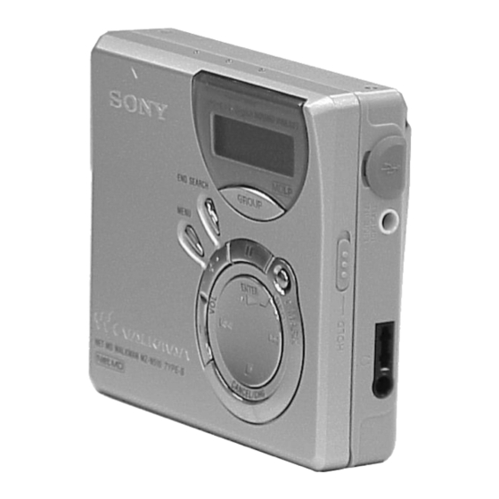
MZ-N510CK
photo : silver model
Model Name Using Similar Mechanism
Mechanism Type
Optical Pick-up Name
Audio playing system
MiniDisc digital audio system
Laser diode properties
Material: GaAlAs
Wavelength: λ = 790 nm
Emission duration: continuous
Laser output: less than 44.6 W
(This output is the value measured at a distance
of 200 mm from the lens surface on the optical
pick-up block with 7 mm aperture.)
Recording and playback time (when
using MDW-80)
Maximum 160 min. in monaural
Maximum 320 min. in LP4 stereo
Revolutions
380 rpm to 2,700 rpm (CLV)
Error correction
ACIRC (Advanced Cross Interleave Reed
Solomon Code)
Sampling frequency
44.1 kHz
Sampling rate converter
Input: 32 kHz/44.1 kHz/48 kHz
Coding
ATRAC (Adaptive TRansform Acoustic
Coding)
ATRAC3 LP 2/LP4
PORTABLE MINIDISC RECORDER
US Model
Canadian Model
Mexican Model
MZ-R410
MT-MZN710-177
LCX-5R
SPECIFICATIONS
– Continued on next page –
Advertisement
Table of Contents

Related Manuals for Sony MZ-N510CK


Summary of Contents for Sony MZ-N510CK
- Page 1 MT-MZN710-177 Optical Pick-up Name LCX-5R • SonicStage, OpenMG and the OpenMG logo, MagicGate, Net MD and the Net MD logo are trademarks of Sony Corporation. SPECIFICATIONS • Microsoft, Windows, Windows NT and Windows Media are trademarks or Audio playing system...
-
Page 2: Battery Life
OPERATION. REPLACE THESE COMPONENTS WITH NE REMPLACER CES COMPOSANTS QUE PAR DES PIÈSES SONY PARTS WHOSE PART NUMBERS APPEAR AS SONY DONT LES NUMÉROS SONT DONNÉS DANS CE MANUEL SHOWN IN THIS MANUAL OR IN SUPPLEMENTS PUB- OU DANS LES SUPPÉMENTS PUBLIÉS PAR SONY. -
Page 3: Table Of Contents
MZ-N510CK TABLE OF CONTENTS CAUTION Use of controls or adjustments or performance of procedures SERVICING NOTES ..........4 other than those specified herein may result in hazardous ra- diation exposure. GENERAL ..............5 On power sources DISASSEMBLY • Use house current, nickel metal hydride 3-1. -
Page 4: Servicing Notes
MZ-N510CK SECTION 1 SERVICING NOTES • In performing the repair with the power supplied to the set, re- NOTES ON HANDLING THE OPTICAL PICK-UP moving the MAIN board causes the set to be disabled. BLOCK OR BASE UNIT In such a case, fix a convex part of the open/close detect switch The laser diode in the optical pick-up block may suffer electro- (S803 on MAIN board) with a tape in advance. -
Page 5: General
MZ-N510CK SECTION 2 This section is extracted from instruction manual. GENERAL Looking at controls The display window of the recorder The recorder A MONO (monaural) indication I Battery indication Shows approximate battery condition. B LP mode indication : Indication for remaining playing... -
Page 6: Disassembly
MZ-N510CK SECTION 3 DISASSEMBLY • This set can be disassembled in the order shown below. 3-1. Disassembly Flow CASE (LOWER) In order to remove mechanism deck, please remove MAIN board and upper panel section. UPPER PANEL SECTION MAIN BOARD LCD MODULE,... -
Page 7: Case (Lower)
MZ-N510CK Note: Follow the disassembly procedure in the numerical order given. 3-2. Case (Lower) 2 two screws (M1.4) 1 two screws (M1.4) 3 Remove the case (lower) in the direction of the arrow. 3-3. Upper Panel Section 1 flexible board... -
Page 8: Lcd Module, Button (Control)
MZ-N510CK 3-4. LCD Module, Button (Control) Note: On installation, adjust the position of 1 six screws both switch and knob (hold). 2 LCD module switch 3 three screws 4 open locker 5 button (control) case (upper) sub assy knob (hold) 3-5. -
Page 9: Mechanism Deck (Mt-Mzn710-177)
MZ-N510CK 3-6. Mechanism Deck (MT-MZN710-177) 1 two step screws (MD) 3 mechanism deck (MT-MZN710-177) The portion which projected is removed. 3-7. Set Chassis Assy 2 two screws (TP 1.7 × 2.5) 4 ground spring (USB) 5 set chassis assy 3 battery case... -
Page 10: Op Service Assy (Lcx-5R)
MZ-N510CK 3-8. OP Service Assy (LCX-5R) 2 gear (SA) 5 screw (M1.4) 1 washer (0.8-2.5) 6 thrust detent spring 3 screw (M1.4) 8 Pull off lead screw. 4 rack spring 9 Opening the over write head toward the direction A , remove the OP service assy (LCX-5R) toward the direction B . -
Page 11: Holder Assy
MZ-N510CK 3-9. Holder Assy 4 holder assy 2 Open the holder assy 3 boss 1 convex portion 3 boss 3-10. DC Motor (Sled) (M602) 2 washer (0.8-2.5) 3 gear (SA) 4 two screws (M1.4) 1 Remove six solders of the motor flexible board. -
Page 12: Dc Motor (Over Write Head Up/Down) (M603)
MZ-N510CK 3-11. DC Motor (Over Write Head Up/Down) (M603), DC SSM18B Motor (Spindle) (M601) 1 Remove six solders of the motor flexible board. 2 tapping screw 3 motor cover 7 DC motor (over write head up/down) (M603) Note: Press-fit the gear (HA) up to the position of the DC motor (over write head up/down) (M603) as shown below. -
Page 13: Test Mode
MZ-N510CK SECTION 4 TEST MODE Outline Operation in Setting the Test Mode • This set provides the Overall adjustment mode that allows CD • When the test mode becomes active, first the display check mode and MO discs to be automatically adjusted when in the test mode. - Page 14 MZ-N510CK Configuration of Test Mode [VOL +] key: 100th place of item number [Major item switching] increase. [Test Mode $Display Check Mode%] [VOL --] key: 100th place of item number [VOL +] Press the key or press the > decrease.
- Page 15 MZ-N510CK [END 5. The display changes a shown below each time the Self-Diagnosis Result Display Mode SEARCH] key is pressed. This set uses the self-diagnostic function system in which if an error occurred during the recording or playing, the mechanism control block and the power supply control block in the •...
- Page 16 MZ-N510CK • Description of Error Indication Codes Problem Indication code Meaning of code Simple display Description No error No error No error Illegal access target Adrs Attempt to access an abnormal address address was specified Servo system error High temperature...
- Page 17 MZ-N510CK Sound Skip Check Result Display Mode • Cause of Sound Skip Error This set can display the count of errors that occurred during the Cause of error Description of error recording/playing for checking. Sound error correction error • Setting Method of Sound Skip Check Result Display...
- Page 18 MZ-N510CK 4. When all the keys on the set and on the remote commander are considered as OK, the following displays are shown. Example1: When the keys on the set are considered as OK: Set LCD display 8 88 S E T O K...
-
Page 19: Electrical Adjustments
TDYS-1 4. Press the xCANCEL/CHG key to quit the manual mode, and (Part No. : 4-963-646-01) return to the test mode (display check mode). • SONY MO disc available on the market • Digital voltmeter • Laser power meter LPM-8001 Temparature Correction (Part No. - Page 20 MZ-N510CK • Adjustment Method of VC1_LOW (PB) • Adjustment Method of VC2_LOW (item number: 741) (item number: 743) Set LCD display Set LCD display 7 41 7 43 A D * * A D * * ** : Adjusted value ** : Adjusted value 1.
- Page 21 MZ-N510CK • Adjustment Method of REG1 • Adjustment Method of REG3_LOW2 (item number: 745) (item number: 748) Set LCD display Set LCD display 7 45 7 48 A D * * A D * * ** : Adjusted value ** : Adjusted value 1.
- Page 22 MZ-N510CK • Adjustment Method of VREC_LOW (X2 speed) • Adjustment Method of VREC_HIGH (HEAD MOTOR) (item number: 751) (item number: 753) Set LCD display Set LCD display 7 51 7 53 A D * * A D * * ** : Adjusted value ** : Adjusted value 1.
- Page 23 MZ-N510CK • Adjustment Method of CHGV_HIGH • Adjustment Method of CHGI_HIGH (Charge current) (item number: 756) (item number: 758) Set LCD display Set LCD display 7 56 7 58 A D * * A D * * ** : Adjusted value ** : Adjusted value Note: Remove the rechargeable battery.
- Page 24 MZ-N510CK Adju s tment/ c hecking and Connection Location: MAIN BOARD (SIDE B) BATT+ TP1909 (REGO1) BATT– TP1898 TP1867 TP1720 TP1805 TP1854 TP1823 TP1852 TP1847 IC361 TP1529 TP1833 TP1523 TP1850 TP1834 R841 TP1311 C540 TP1830 TP1528 (GND) TP1511 SL502 TP1831...
- Page 25 MZ-N510CK Power Supply Adjustment Auto Item Feed Set LCD display Note: This mode is available to perform the temperature correction and power supply adjustment without entering the manual mode. 7 41 V C 1 L • Setting method of power supply adjustment auto item feed mode.
- Page 26 MZ-N510CK Laser Power Check and Adjustment 13. Press the key, and set the laser MO (X4 speed) write ad- > justment mode (item number 014). • Connection laser Set LCD display power meter 0 14 # # # S * *...
- Page 27 MZ-N510CK [VOL +] [VOL --] 12. Adjust with the key (adjusted value up) or key (adjusted value down) so that the adjusted value becomes 13. Press the X key on the set or press the key on the remote commander to write the adjusted value.
- Page 28 MZ-N510CK • Adjustment Method of CD and MO Overall Adjustment 8. If OK through the MO overall adjustments, press Mode key to return to the test mode and ter- xCANCEL/CHG 1. Set the test mode (see page 13). minate the overall adjustment mode.
- Page 29 MZ-N510CK Item No. Description Item No. Description Two-axis sensitivity (outer position) Focus gain adjustment HPIT setting . servo OFF Tracking gain adjustment TWPP gain adjustment 2. MO overall adjustment items TWPP offset adjustment 1 Item No. Description TE offset adjustment 2...
- Page 30 MZ-N510CK Remuse Clear Perform the Resume clear when all adjustments completed. • Resume Clear Setting Method 1. Select the manual mode of the test mode, and set item number 043 (see page 14). Set LCD display 0 43 # # # S 0 0 ### : Address 2.
- Page 31 MZ-N510CK Rewriting the Patch Data at Replacement of Main Board This set requires the patch data in the nonvolatile memory (IC852) to be rewritten using the application, when the MAIN board was replaced. Cau t ion: The application that meets the microcomputer version in this set must be used when rewriting the patch data. Rewriting the patch data using the application not suitable for the microcomputer version could cause the set to malfunction.
- Page 32 MZ-N510CK 5. Confirm that the model and version indicated on the title bar coincide with the codes displayed in the Device Name block and the Version block in the window. 6. Click the [Write + Read] button. The patch data writing and the verify processing will be executed automatically in the following order:...
- Page 33 MZ-N510CK • Confirmation of contents of the patch data rewrited 1. Click the [READ] button to confirm the contents of the patch data rewrited. 2. The application reads out the front and reverse patch areas and displays the results in the edit box.
- Page 34 MZ-N510CK • Disconnecting the USB cable Disconnect the USB cable as the following procedure after rewriting the patch data and confirmation. Note : When the following procedure is not completed but USB cable is extracted, the application does not recognize the set at exchanging of the set.
- Page 35 MZ-N510CK Rewriting the NV values Cau t ion: The application that meets the microcomputer version in this set must be used when rewriting the NV values. Rewriting the NV values using the application not suitable for the microcomputer version could cause the set to malfunction.
- Page 36 MZ-N510CK 5. Confirm that the model and version indicated on the title bar coincide with the codes displayed in the Device Name block and the Version block in the window. 6. Click the [Write + Verify] button. The NV values writing and the verify processing will be executed automatically in the following order:...
- Page 37 MZ-N510CK 7. The operation will terminate with “Compere OK” given to all areas. If “Compere NG” is given to any area, the nonvolatile memory will be faulty. 8. Click the [USB DISCONNECT] button.
- Page 38 MZ-N510CK 9. Confirm that the window becomes as shown below where the [Write + Verify] button is inactive. 10. Disconnect the USB cable from the personal computer and the set.
-
Page 39: Diagrams 6-1. Block Diagram
MZ-N510CK SECTION 6 DIAGRAMS 6-1. Block Diagram SYSTEM CONTROLLER SYSTEM CONTROLLER HP AMP DIGITAL SIGNAL PRCESSOR RF AMP DIGITAL SIGNAL PRCESSOR POWER AMP IC361 IC501 IC801(1/2) IC801(2/2) IC901 REGO1 VREF VREF IN Q361 OPTICAL PICK-UP DVCC REGO1 IFVDD0 DATA SDO0... -
Page 40: Note For Printed Wiring Board And Schematic Diagrams
MZ-N510CK 6-2. Note For Printed Wiring Board And Schematic Diagrams • Waveforms Note on Printed Wiring Board: Note on Schematic Diagram: IC501 9 (RFO)(TP1517) IC601 4 (CLK) IC901 yd (CLK) IC302 qs (LRCK) • X : parts extracted from the component side. -
Page 41: Main Board (Side A)
MZ-N510CK 6-3. Printed Wiring Board – MAIN Board (Side A) – :Uses unleaded solder. • Semiconductor Location Ref. No. Location D606 S801 D607 (HALF LOCK) D653 D654 MAIN BOARD (SIDE A) D953 D958 IC302 IC701 Q501 CN651 Q603 Q604 Q605... -
Page 42: Main Board (Side B)
MZ-N510CK 6-4. Printed Wiring Board – MAIN Board (Side B) – :Uses unleaded solder. • Semiconductor Location Ref. No. Location MAIN BOARD (SIDE B) D101 D201 D302 D303 D605 S806 D652 (PROTECT) D901 D902 D903 D952 M602 (SLED) D955 D960... -
Page 43: Schematic Diagram - Main Board (1/4)
MZ-N510CK 6-5. Schematic Diagram – MAIN Board (1/4) – • • See page 40 for Waveforms. See page 49 and 51 for IC Block Diagrams. C630 0.1 B C631 47 4V Q605 CPH5614 D606 MA2YD1700LS0 C632 100p D607 MA2YD1700LS0 Q604... -
Page 44: Schematic Diagram - Main Board (2/4)
MZ-N510CK 6-6. Schematic Diagram – MAIN Board (2/4) – • • See page 40 for Waveform. See page 48 and 50 for IC Block Diagrams. C513 C524 0.022 TP1539 C517 0.01 TP518 R511 CN501 C535 C526 C718 C720 TP1504 0.047... -
Page 45: Schematic Diagram - Main Board (3/4)
MZ-N510CK 6-7. Schematic Diagram – MAIN Board (3/4) – • • See page 40 for Waveforms. See page 52 for IC Pin Function Description. R821 R822 R824 220k 470k FB802 R826 C819 2.2k R858 C834 1000p X802 0.022 R827 48MHz 4.7k... -
Page 46: Schematic Diagram - Main Board (4/4)
MZ-N510CK 6-8. Schematic Diagram – MAIN Board (4/4) – • • See page 40 for Waveforms. See page 47 for IC Block Diagrams. J302 J303 CN871 TP1881 TP1882 TP1883 TP1884 TP1885 D201 TP1886 02DZ2.4-Z(TPH3) TP1887 D101 02DZ2.4-Z(TPH3) TP1888 TP1889 R315... -
Page 47: Ic Block Diagrams
MZ-N510CK • IC Block Diagrams IC302 AK5354VT-E2 16 PDN LIN1 15 CSN CONTROL IPGA 14 CCLK RIN1 REGISTER LIN2 13 CDTI RIN2 CLOCK DIVIDER VCOM 12 LRCK AGND 11 MCLK AUDIO I/F CONTROLLER 10 BCLK 9 STDD IC361 TA2131FL (EL) - Page 48 MZ-N510CK IC501 SN761058ZQLR AVCC PEAK/ OFTRK T-ON BOTM 42 FE ABCD 41 ABCD 40 RFI A GND 39 ASSY OFC-C1 38 CIG TPP/WPP OFC-C2 37 EFMO VREF10 DGND RESET 34 VGIN VREF09 33 SBUS AVCC2 AVCC2 32 SCK PD-NI CPOUT...
- Page 49 MZ-N510CK IC601 XPC18A22AEPR2 VC2 VG OUTPUT SW OUTPUT SW CHARGE CHARGE PUMP 1 PUMP 2 VC VG DC IN HI-BRIDGE CHARGE PRE DRIVER PRE DRIVER MONITOR VREF VREF X2/X4 BATM BUFFER DC IN CVREF CONTROL CONTROL CHARGE CHGSW DW BT...
- Page 50 MZ-N510CK IC701 SC111258EPR2 48 47 46 45 52 51 3Phase BIAS control 3Phase control PGNDW2 VG VC PGNDW1 VMVW2 3Phase Pre driver WMVW1 3Phase Pre driver PGNDUV2 PGNDUV1 35 UO2 VMU2 VMR2 VMU1 VG VC VMR1 H-BRIDGE PGND2 DRIVER H-BRIDGE...
- Page 51 MZ-N510CK IC901 SC901580EPR2 (HP AMP) AMP1 CONTROL BANDGAP FFCLR1 48 VREF REFERENCE XWAKE4 47 REGC3 REF1 XWAKE3 46 REGC2 REF2 REF3 XWAKE2 45 REGC1 REF4 REF5 XWAKE1 44 REGI1 SERIES PASS REGULATOR1 REF3 VRMC 43 REGO1 FFCLR 42 VC2 SERIES PASS...
-
Page 52: Ic Pin Function Description
MZ-N510CK 6-9. IC Pin Function Description • IC801 CXD2680-203GA (SYSTEM CONTROLLER, DIGITAL SIGNAL PROCESSOR) Pin No. Pin Name Description OSCI Resonator connection terminal for the system clock (22.5792MHz) OSCO Resonator connection terminal for the system clock (22.5792MHz) VREFL Reference voltage terminal connected to the capacitor (for the built-in D/A converter L-CH) - Page 53 MZ-N510CK Pin No. Pin Name Description ADDT Data input from the external A/D converter KRCK L/R sampling clock (44.1KHz) output to the external A/D converter XBCK Bit clock (2.8224MHz) output to the external A/D converter FS256 11.2896MHz clock output Filter cutoff control signal output Not used (open)
- Page 54 MZ-N510CK Pin No. Pin Name Description BATT_CTL Control signal output for the voltage step up circuit in the external battery case Not used (open) VREC_CTL VREC voltage control signal output Not used (open) XRST_CHG_IC Reset signal output to the battery charge control IC...
- Page 55 MZ-N510CK Pin No. Pin Name Description WK_DET Set key WAKE detection signal input BATT_MON External battery voltage monitor input Not used (connected to the ground) HALF_LOCK_SW Open button detection switch input (A/D input) “L” : the open button is pressed...
- Page 56 MZ-N510CK Pin No. Pin Name Description — DRAM chip select terminal Not used (open) — DRAM clock terminal Not used (open) — DRAM clock enable terminal Not used (open) UDQM — DRAM byte mask terminal Not used (open) LDQM —...
- Page 57 MZ-N510CK Pin No. Pin Name Description FVDD0 — Power supply terminal (for the built-in flash memory) FVSS0 — Ground terminal (for the built-in flash memory) 301, 302 DVDD5, 6 — Power supply terminal 303, 304 DRAMVDD3, 4 — Power supply terminal (for DRAM) MSAK —...
-
Page 58: Exploded Views
MZ-N510CK SECTION 7 EXPLODED VIEWS NOTE: • -XX and -X mean standardized parts, so they • Items marked “*” are not stocked since they The components identified by mark 0 or may have some difference from the original are seldom required for routine service. Some dotted line with mark 0 are critical for safety. -
Page 59: Chassis Section
MZ-N510CK 7-2. Chassis Section MT-MZN710-177 not supplied MAIN board section Ref. No. Part No. Description Remark Ref. No. Part No. Description Remark 3-237-072-02 SCREW (MD), STEP 3-318-382-91 SCREW (1.7X2.5), TAPPING X-3382-628-1 CHASSIS ASSY, SET 3-246-245-01 SLIDER, OPEN 3-249-532-01 SPRING (POP UP-L), TORSION... -
Page 60: Main Board Section
MZ-N510CK 7-3. MAIN Board Section Ref. No. Part No. Description Remark Ref. No. Part No. Description Remark 3-246-247-01 CASE, BATTERY A-3663-986-B MAIN BOARD, COMPLETE(CND,MX) 3-237-073-01 TERMINAL BOARD (+), BATTERY 3-253-535-01 SHEET (DC-IN) 3-237-074-11 TERMINAL (–), BATTERY 3-253-534-01 CUSHION (H/J) A-3347-683-B MAIN BOARD, COMPLETE... -
Page 61: Mechanism Deck Section-1 (Mt-Mzn710-177)
MZ-N510CK 7-4. Mechanism Deck Section-1 (MT-MZN710-177) mechanism deck section-2 not supplied Ref. No. Part No. Description Remark Ref. No. Part No. Description Remark X-3381-219-1 HOLDER ASSY 3-043-237-02 BEARING (N) 3-224-779-02 SPRING, THRUST DETENT 4-222-203-02 SCREW, LEAD 3-225-996-01 SCREW (M1.4) (EG), PRECISION PAN... -
Page 62: Mechanism Deck Section-2 (Mt-Mzn710-177)
MZ-N510CK 7-5. Mechanism Deck Section-2 (MT-MZN710-177) M602 M603 supplied M601 Ref. No. Part No. Description Remark Ref. No. Part No. Description Remark 3-225-278-12 SCREW, TAPPING 3-338-645-31 WASHER (0.8-2.5) 3-235-838-01 COVER, MOTOR 4-222-222-01 GEAR (RACK) 3-235-836-01 GEAR (HB) A-3174-089-A SHAFT BLOCK ASSY, SUB... -
Page 63: Electrical Parts List
MZ-N510CK SECTION 8 ELECTRICAL PARTS LIST MAIN NOTE: • Due to standardization, replacements in the • Items marked “*” are not stocked since they The components identified by mark 0 or parts list may be different from the parts speci- are seldom required for routine service. - Page 64 MZ-N510CK MAIN Ref. No. Part No. Description Remark Ref. No. Part No. Description Remark C632 1-137-760-91 CAP-CHIP 100PF 100V C906 1-164-937-11 CERAMIC CHIP 0.001uF 10.00% 50V C658 1-137-739-91 TANTALUM 22uF 6.3V C907 1-125-889-91 CERAMIC CHIP 2.2uF C659 1-164-937-11 CERAMIC CHIP 0.001uF...
- Page 65 MZ-N510CK MAIN Ref. No. Part No. Description Remark Ref. No. Part No. Description Remark D952 6-500-483-01 DIODE MA22D2800LS0 < TRANSISTOR > D953 6-500-483-01 DIODE MA22D2800LS0 D955 6-500-483-01 DIODE MA22D2800LS0 Q301 8-729-051-23 TRANSISTOR 2SA2018TL D958 8-719-017-58 DIODE MA8068-TX Q361 8-729-037-52 TRANSISTOR...
- Page 66 MZ-N510CK MAIN Ref. No. Part No. Description Remark Ref. No. Part No. Description Remark R312 1-218-989-11 RES-CHIP 1/16W R823 1-208-643-11 RES-CHIP 1/16W R315 1-218-990-11 SHORT CHIP R824 1-218-985-11 RES-CHIP 470K 1/16W R361 1-218-937-11 RES-CHIP 1/16W R362 1-218-981-11 RES-CHIP 220K 1/16W...
- Page 67 MZ-N510CK MAIN Ref. No. Part No. Description Remark Ref. No. Part No. Description Remark R955 1-218-941-81 RES-CHIP 1/16W MISCELLANEOUS R956 1-208-943-11 METAL CHIP 220K 0.5% 1/16W *************** R957 1-208-927-11 METAL CHIP 0.5% 1/16W R959 1-208-935-11 METAL CHIP 100K 0.5% 1/16W...
- Page 68 MZ-N510CK REVISION HISTORY Clicking the version allows you to jump to the revised page. Also, clicking the version at the upper right on the revised page allows you to jump to the next revised page. Ver. Date Description of Revision...