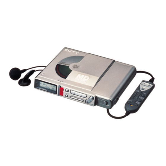
Sony MZ-R37 Service Manual
Portable minidisc recorder
Hide thumbs
Also See for MZ-R37:
- Operating instructions manual (76 pages) ,
- Specification sheet (2 pages) ,
- Operating instructions manual (40 pages)
Table of Contents
Advertisement
SERVICE MANUAL
Ver 1.3 1999. 11
With SUPPLEMENT-1
(9-926-952-81)
With SUPPLEMENT-2
(9-926-952-82)
US and foreign patents licensed from Dolby Laboratories
Licensing Corporation.
System
Audio playing system
MiniDisc digital audio system
Laser diode properties
Material: GaAlAs
Wavelength: λ = 780 nm
Emission duration: continuous
Laser output: less than 44.6 µW
(This output is the value measured at a
distance of 200 mm from the lens surface on
the optical pick-up block with 7 mm
aperture.)
Recording and playback time
Maximum 74 minutes (MDW-74, stereo
recording)
Maximum 148 minutes (MDW-74, monaural
recording)
Revolutions
400 rpm to 900 rpm (CLV)
Error correction
Advanced Cross Interleave Reed Solomon
Code (ACIRC)
Sampling frequency
44.1 kHz
Sampling rate converter
Input: 32 kHz / 44.1 kHz / 48 kHz
Coding
Adaptive TRansform Acoustic Coding (ATRAC)
Modulation system
EFM (Eight to Fourteen Modulation)
Number of channels
2 stereo channels
1 monaural channel
MICROFILM
MZ-R37
Model Name Using Similar Mechanism
MiniDisc Mechanism Type
Optical Pick-up Type
SPECIFICATIONS
Frequency response
20 to 20,000 Hz ± 3 dB
Wow and Flutter
Below measurable limit
Inputs
MIC (PLUG IN POWER): stereo mini-jack,
0.35–1.38 mV
(OPTICAL) LINE IN: stereo mini-jack with
optical (digital) in
• Line in: 69–194 mV
• Optical (digital) in: wave length 660 nm
Outputs
PHONES/REMOTE: stereo mini-jack,
maximum output level 5 mW + 5 mW, load
impedance 16 ohm
LINE OUT: stereo mini-jack, 194 mV, load
impedance 10 kilohm or greater
General
Power requirements
Sony AC Power Adaptor (supplied)
connected at the DC IN 4.5 V jack:
120 V AC, 60 Hz (US, Canadian model)
220–230 V AC, 50/60 Hz (AEP model)
230–240 V AC, 50 Hz (UK model)
240 V AC, 50 Hz (Australian and New Zealand model)
Two nickel-cadmium rechargeable batteries
NC-AA (supplied)
Two LR6 (size AA) alkaline batteries (not supplied)
PORTABLE MINIDISC RECORDER
– 1 –
US Model
Canadian Model
AEP Model
UK Model
E Model
Australian Model
Tourist Model
MZ-R55
MT-MZR37-161
KMS-280A
– Continued on next page –
Advertisement
Chapters
Table of Contents

Related Manuals for Sony MZ-R37


Summary of Contents for Sony MZ-R37
- Page 1 Revolutions General 400 rpm to 900 rpm (CLV) Power requirements Error correction Sony AC Power Adaptor (supplied) Advanced Cross Interleave Reed Solomon connected at the DC IN 4.5 V jack: Code (ACIRC) 120 V AC, 60 Hz (US, Canadian model) Sampling frequency 220–230 V AC, 50/60 Hz (AEP model)
- Page 2 REPLACE THESE COMPONENTS WITH SONY PARTS WHOSE CRITIQUES POUR LA SÉCURITÉ DE FONCTIONNEMENT. NE PART NUMBERS APPEAR AS SHOWN IN THIS MANUAL OR IN REMPLACER CES COMPOSANTS QUE PAR DES PIÈCES SONY SUPPLEMENTS PUBLISHED BY SONY. DONT LES NUMÉROS SONT DONNÉS DANS CE MANUEL OU DANS LES SUPPLÉMENTS PUBLIÉS PAR SONY.
-
Page 3: Table Of Contents
TABLE OF CONTENTS 1. GENERAL 4. TEST MODE Looking at the controls ............4 4-1. General ................12 4-2. Test Mode Setting ............12 4-3. Test Mode Structure ............12 2. SELF-DIAGNOSTIC 4-4. Manual Mode ..............12 2-1. General ................5 4-5. -
Page 4: General
SECTION 1 GENERAL This section is extracted from instruction manual. – 4 –... -
Page 5: Self-Diagnostic
SECTION 2 SELF-DIAGNOSTIC 2-1. GENERAL 2) Remote controller LCD This set uses the self-diagnostic system in which if an error occurs in playback/recording mode, the error is detected by the model control and power control blocks of the microprocessor and infor- mation on the cause is stored as history in EEPROM. -
Page 6: Clearing The Error Indication Code And Total Recording Time
• Description of History Codes History code number Description The first error 00 indicated The last error 00 indicated *1) Total recording time One error before the last. Total recording time is recorded in minutes as an index for load to the OP. -
Page 7: Disassembly
SECTION 3 DISASSEMBLY Note : This set can be disassemble according to the following sequence. Panel, Panel (SV) Assy, LCD Module Bottom Front Connector Main Panel (SV) Assy, Cabinet (SV) OP Block Holder Board Upper Assy Assy Assy Note : Follow the disassembly procedure in the numerical order given. 3-1. -
Page 8: Lcd Module
3-3. LCD MODULE 1 CN801 5 LCD module 3-4. CONNECTOR 1 CN601 2 CN702 3 CN701 – 8 –... -
Page 9: Main Board
3-5. MAIN BOARD 1 1.7x4.5, tapping 2 1.7x4.5, tapping MAIN board claws 3-6. PANEL (SV) ASSY, UPPER 1 M1.4, precision 8 panel (SV) assy, upper 3 bearing (stopper) 4 claw 6 boss 5 claw – 9 –... -
Page 10: Cabinet (Sv) Assy
3-7. CABINET (SV) ASSY 1 MD, step 4 cabinet (SV) assy 2 MD, step 3 mechanism block assy 3-8. OP BLOCK ASSY 1 M1.4x3.0 locking 2 M1.4x3.0 3 shaft, main adhesive sheet OP block assy 4 flexible board – 10 –... -
Page 11: Holder Assy
• Notes for Installation of the OP Block Assy • Be careful to avoid contact of the lens with the chassis • Location of the Flexible Board when installing the OP block assy. marked line Align this portion of the flexible board with the marked line on the holder. -
Page 12: Test Mode
SECTION 4 TEST MODE 4-1. GENERAL Mode No. Test Description Check Write This set provides the Overall adjustment mode (Assy mode) that ® ® (00) Low reflection CD focus bias allows CD and MO disk to be automatically adjusted when in the CD test adjustment test mode. - Page 13 (2) Audio Mode 2. To perform automatic adjustment for an adjustment item with the mode number 030 to 047, press P key. • How to Transfer in the Audio Mode If the result of adjustment is OK, the adjustment value changes Change Mode No.
- Page 14 Unit LCD display (3) Mechanism Mode • How to Transfer the Mode in the Mechanism Mode: Mode No. Test Description Operation FUNCTION Stepper control XX XX AUDIO MECHA test Initial position return HEAD adjustment Operation variation changing (19) REC position Recording head descent Adjustment value RESUME...
-
Page 15: Overall Adjustment Mode (Assy Mode)
BATT under +B CHGMNT voltage value 3. Insert the test CD (TDYS-1) or an available SONY CD. 1. Go into the test mode. 4. Press ( key. The system discriminates between CD and MO 2. Press + key or VOLUME + and VOLUME + and VOL- and performs automatic adjustment for CD. -
Page 16: Hybrid Mode, Key Check Mode
* For the mode numbers of 039 and 057, if the focus bias value is 10. If the result of automatic adjustment is OK, the following dis- NG, the following display is repeated: play appears: 55 30 Focus bias value 11. -
Page 17: Electrical Adjustments
SECTION 5 ELECTRICAL ADJUSTMENTS PRECAUTIONS FOR ADJUSTMENT MO TRAVERSE ADJUSTMENT 1) Perform all adjustments in the order given in the test mode. Connection : After adjusting, exit the test mode. 2) Use the following tools and measuring instruments. oscilloscope • Test CD TDYS-1 MAIN board (Part No. - Page 18 LOW REFLECTION CD TRAVERSE ADJUSTMENT CD TRAVERSE ADJUSTMENT Connection : Connection : oscilloscope oscilloscope MAIN board MAIN board SP526 (TE) SP526 (TE) AP503 (VC) AP503 (VC) Adjustment Method : Adjustment Method : 1. Set the servo mode of the test mode (Mode : 000). 1.
- Page 19 CD RF LEVEL CHECK Adjustment Location : Connection : oscilloscope MAIN BOARD (SIDE B) MAIN board AP538 (RF) AP503 (VC) digital voltmeter MAIN board AP5117 (VCC) IC701 AP574 (LDIO) AP538 (RF) Adjustment Method : 1. Set the servo mode of the test mode (Mode : 000). AP574 (LDIO) 2.
-
Page 20: Diagrams
SECTION 6 DIAGRAMS 6-1. IC PIN DESCRIPTIONS • IC601 CXD2652AR (DIGITAL SERVO, ENC/DEC & ATRAC MEMORY CONTROLLER) Pin No. Pin name Pin Description MNT 0 Traverse count signal output. MNT 1 Track jump detect output. MNT 2 — Not used (Open). MNT 3 Focus OK signal output. - Page 21 Pin No. Pin name Pin Description AVSS — Ground terminal. — Not used (Open). Decoder PLL master clock PLL phase comparison output. FILI Decoder PLL master clock PLL filter input. FILO Decoder PLL master clock PLL filter output. CLTV Decoder PLL master clock PLL VCO control voltage input. PEAK Inputs peak hold signal for light amount signal from RF amplifier (IC501).
- Page 22 • IC801 CXP740010 (SYSTEM CONTROL) Pin No. Pin name Pin Description CLKCS Not used (Chip select output to real time clock). XRST Reset output. L : Reset WRPWR Laser power switching signal output. Write data transfer timing output. SDI2 Serial data input. SDO2 Serial data output.
- Page 23 Pin No. Pin name Pin Description — Ground terminal for A/D converter. AVREF A/D converter reference voltage input. — A/D converter power supply terminal. VLG2-MNT DSP power monitor signal. TEMP Temp meter (IC802) input. KEY3 Key input. KEY2 Key input. KEY1 Key input.
-
Page 24: Block Diagram - Servo Section
MZ-R37 6-2. BLOCK DIAGRAM — SERVO SECTION — REC DRIVE DIGITAL SERVO ENC/DEC IC901 (1/2) & MODE1 ATRAC MEMORY CONTROLER DRAM IC601 MODE2 IC602 OVER OVER WRITE EFMO WRITE HEAD DRIVE LOGIC HEAD Q741,742 XRAS XRAS XCAS XCAS EFM/ ACIRC... -
Page 25: Block Diagram - Audio Section
MZ-R37 6-3. BLOCK DIAGRAM — AUDIO SECTION — 6-4. BLOCK DIAGRAM — SYSTEM CONTROL SECTION — AUDIO KEYRMC 2.8V CONTROL SECTION Q302 (Page 27) SYSTEM CONTROL POWER CONTROL IC801 (3/3) IC901 J301 LCD RESET LINE IN SERVO A/D, D/A (OPTICAL) -
Page 26: Printed Wiring Board
MZ-R37 6-5. PRINTED WIRING BOARD • Semiconductor Location Ref. No. Location D401 D402 D403 D404 H-25 D406 D407 D-26 D408 F-26 D741 B-20 D742 C-20 D801 G-22 D901 H-17 D902 H-16 D903 H-19 D904 G-17 D905 H-19 D906 G-11 D907... -
Page 27: Schematic Diagram - Main Section (1/3)
MZ-R37 • Waveforms 6-6. SCHEMATIC DIAGRAM — MAIN SECTION (1/3) — • Refer to page 44 for IC Block Diagrams. VOLT/DIV : 0.5V AC TIME/DIV : 1µsec 1.0±0.3Vp-p #• IC501 VOLT/DIV : 0.1V AC TIME/DIV : 0.1msec Approx. 0.5Vp-p @ª... -
Page 28: Schematic Diagram - Main Section (2/3)
MZ-R37 6-7. SCHEMATIC DIAGRAM — MAIN SECTION (2/3) — • Refer to page 44 for IC Block Diagrams. • Waveform VOLT/DIV : 1V AC TIME/DIV : 20nsec (Page 43) (Page 42) 2.2Vp-p (Page 37) (Page 37) 12kHz $º IC801 (Page 37) -
Page 29: Schematic Diagram - Main Section (3/3)
MZ-R37 6-8. SCHEMATIC DIAGRAM — MAIN SECTION (3/3) — • Refer to page 44 for IC Block Diagrams. (Page 37) (Page 37) (Page 38) (Page 38) (Page 37) (Page 38) Note: • All capacitors are in µF unless otherwise noted. pF: µµF •... - Page 30 • IC Block Diagrams IC501 CXA2523AR IC602 MN41X4400TT-10TIL IC301 AK4517-VQ-L 43 42 DQ0 1 USROP – DQ1 2 47 46 RF AGC WE 3 – WRITE USRC RFA1 CLOCK CLOCK RAS 4 GENERATOR GENERATOR IPGAL CLOCK BPF3T MCLK DIVIDER RFA2 RFA3 PEAK3T –...
- Page 31 IC761 BA6966FV-E2 VOUT WOUT STBY BRK+ BRK- STAND-BY PREDRIVE UP-DOWN DISTRIBUTION EX-OR DRIVING SIGNAL COMPOSITION LOGIC TIMING SELECTOR START SLOBE PHASE CONTROL WAVE CONTROL LOGIC COMPOSITION UOUT RF CSL1 CSL2 IC803 AK6420AM-E DATA REGISTER R/W AMPS AUTO ERASE INSTRUCTION EEPROM REGISTER 2048bit 128x16...
- Page 32 IC901 MPC18A35FTA 46 45 44 43 40 39 38 37 DCIN GENERATOR PSL1 POWER SW PRE-DRIVER PSAM DGND VAM3 DCIN DC IN VLG2 PRE-DRIVER CHARGE VLG1 PUMP PRE-DRIVER DRIVE PGND CONTROL PGND REMGND PGND3 REMKEY KEYON SETUP REGULATOR DC/DC SYNC INMU WAKEO SYSTEM...
-
Page 33: Exploded Views
SECTION 7 EXPLODED VIEWS NOTE: • The mechanical parts with no reference • -XX and -X mean standardized parts, so The components identified by number in the exploded views are not supplied. they may have some difference from the mark ! or dotted line with mark. •... -
Page 34: Cabinet (Sv) Assy Section
7-2. CABINET (SV) ASSY SECTION MT-MZR37-161 LCD1 Ref. No. Part No. Description Remark Ref. No. Part No. Description Remark X-4951-496-1 CABINET (S) ASSY (SILVER) 4-216-598-01 SPRING, BATTERY COIL X-4951-497-1 CABINET (L) ASSY (BLUE) (EXCEPT US,CND) 4-212-820-01 DAMPER 4-963-883-41 SCREW (M1.4), PRECISION PAN 4-982-382-11 SCREW (MD), STEP X-4950-927-1 PLATE ASSY, FULCRUM 4-216-585-01 SCREW, STEP... -
Page 35: Mechanism Deck Section
7-3. MECHANISM DECK SECTION (MT-MZR37-161) The components identified by Les composants identifiés par une mark ! or dotted line with mark. marque ! sont critiques pour la ! are critical for safety. sécurité. Replace only with part number Ne les remplacer que par une piéce specified. -
Page 36: Electrical Parts List
SECTION 8 MAIN ELECTRICAL PARTS LIST NOTE: • Due to standardization, replacements in • Items marked “*” are not stocked since The components identified by the parts list may be different from the they are seldom required for routine service. mark ! or dotted line with mark. - Page 37 MAIN Ref. No. Part No. Description Remark Ref. No. Part No. Description Remark C511 1-115-467-11 CERAMIC CHIP 0.22uF C825 1-162-969-11 CERAMIC CHIP 0.0068uF 10% C512 1-162-968-11 CERAMIC CHIP 0.0047uF 10% C851 1-162-970-11 CERAMIC CHIP 0.01uF C513 1-162-970-11 CERAMIC CHIP 0.01uF C852 1-107-826-11 CERAMIC CHIP 0.1uF...
- Page 38 MAIN Ref. No. Part No. Description Remark Ref. No. Part No. Description Remark D801 8-719-045-67 DIODE RB731U-T108 L703 1-410-389-31 INDUCTOR CHIP 47uH D901 8-719-066-16 DIODE RB491D-T146 L704 1-410-389-31 INDUCTOR CHIP 47uH D902 8-719-047-73 DIODE HRU0302A-TR L705 1-410-389-31 INDUCTOR CHIP 47uH D903 8-719-047-73 DIODE HRU0302A-TR L706...
- Page 39 MAIN MAIN Ref. No. Part No. Description Remark Ref. No. Part No. Description Remark R202 1-218-875-11 RES,CHIP 0.50% 1/16W R424 1-216-809-11 METAL CHIP 1/16W (EXCEPT FR) R461 1-216-864-11 METAL CHIP 1/16W R203 1-218-855-11 RES,CHIP 2.2K 0.50% 1/16W R462 1-216-864-11 METAL CHIP 1/16W R205 1-218-863-11 RES,CHIP...
- Page 40 MZ-R37 MAIN Ref. No. Part No. Description Remark Ref. No. Part No. Description Remark R816 1-216-864-11 METAL CHIP 1/16W S803 1-771-138-21 SWITCH, KEY BOARD (T.MARK) R818 1-216-851-11 METAL CHIP 330K 1/16W S804 1-762-078-11 SWITCH, SLIDE (SYNCHRO REC) R819 1-216-851-11 METAL CHIP...
- Page 41 Subject : Korean model Addition Korean model is added to the MZ-R37. This supplement-1 describes only differences from the MZ-R37 (E) model. Refer to the service manual for MZ-R37 (9-926-952-∏) for other information. • ACCESSORIES & PACKING MATERIALS Page MZ-R37 (E model) MZ-R37 (Korean model) Part No.
- Page 42 MZ-R37 TABLE OF CONTENTS 1. PRINTED WIRING BOARD US Model – EXCEPT US MODEL – ..........3 Canadian Model 2. PRINTED WIRING BOARD SERVICE MANUAL AEP Model – US MODEL – ..............7 UK Model 3. SCHEMATIC DIAGRAM – MAIN SECTION (1/3) –...
-
Page 43: Printed Wiring Board - Except Us Model
MZ-R37 1. PRINTED WIRING BOARD — EXCEPT US MODEL — MAIN BOARD (SIDE A) Note: R412 C427 • Y : parts extracted from the conductor side. R829 TP334 • b : Pattern from the side which enables seeing. TP7114 TP331 (The other layer’s patterns are not indicated.) - Page 44 MZ-R37 • Semiconductor Location MAIN BOARD (SIDE B) MECHANISM J303 Ref. No. Location BLOCK D404 (PULG IN POWER) CN701 D407 R319 OVER WRITE R960 D408 R825 R805 C327 HEAD IC304 C743 R957 D409 CN702 R311 C218 1 2 3 C825...
-
Page 45: Printed Wiring Board - Us Model
MZ-R37 2. PRINTED WIRING BOARD — US MODEL — MAIN BOARD (SIDE A) Note: R412 C427 • Y : parts extracted from the conductor side. R829 TP334 • b : Pattern from the side which enables seeing. TP7114 TP331 (The other layer’s patterns are not indicated.) - Page 46 MZ-R37 • Semiconductor Location MAIN BOARD (SIDE B) MECHANISM J303 Ref. No. Location BLOCK D404 (PULG IN POWER) CN701 R319 D407 OVER WRITE R960 D408 R825 R805 HEAD C327 IC304 C743 R957 D409 CN702 R311 C218 1 2 3 C825...
- Page 47 MZ-R37 3. SCHEMATIC DIAGRAM — MAIN SECTION (1/3) — • Refer to page 15 for Waveforms. • Difference of Schematic Diagram (US Model) (Page 19) (Page 15) (Page 15) Note: • All capacitors are in µF unless otherwise noted. pF: µµF...
-
Page 48: Schematic Diagram - Main Section (1/3)
MZ-R37 4. SCHEMATIC DIAGRAM — MAIN SECTION (2/3) — • Waveforms VOLT/DIV : 0.5V AC (Page 20) TIME/DIV : 1µsec (Page 19) (Page 14) 1.0±0.3Vp-p (Page 14) (Page 14) IC501 VOLT/DIV : 0.1V AC TIME/DIV : 0.1msec Approx. 0.5Vp-p IC501... -
Page 49: Schematic Diagram - Main Section (2/3)
MZ-R37 5. SCHEMATIC DIAGRAM — MAIN SECTION (3/3) — (Page 14) (Page 14) (Page 15) (Page 15) (Page 15) (Page 15) Note: • All capacitors are in µF unless otherwise noted. pF: µµF • Power voltage is dc 4.5 V and fed with regulated dc power •... -
Page 50: Electrical Parts List
MAIN 6. ELECTRICAL PARTS LIST NOTE: • Due to standardization, replacements in • Items marked “*” are not stocked since When indicating parts by reference the parts list may be different from the they are seldom required for routine service. number, please include the board. - Page 51 MAIN Ref. No. Part No. Description Remark Ref. No. Part No. Description Remark C504 1-162-966-11 CERAMIC CHIP 0.0022uF 10% C807 1-162-927-11 CERAMIC CHIP 100PF C505 1-162-970-11 CERAMIC CHIP 0.01uF C808 1-164-156-11 CERAMIC CHIP 0.1uF C506 1-107-826-11 CERAMIC CHIP 0.1uF C810 1-162-970-11 CERAMIC CHIP 0.01uF C507...
- Page 52 MAIN Ref. No. Part No. Description Remark Ref. No. Part No. Description Remark D403 8-719-068-83 DIODE MAZL068D0LS0-TX/L J304 1-778-179-11 JACK (PHONES/REMOTE) D404 8-719-017-58 DIODE MA8068 J901 1-778-153-11 JACK, DC (POLARITY UNIFIED TYPE) D406 8-719-017-58 DIODE MA8068 (DC IN 4.5V) D407 8-719-017-58 DIODE MA8068 D408 8-719-017-58 DIODE MA8068...
- Page 53 MAIN Ref. No. Part No. Description Remark Ref. No. Part No. Description Remark R112 1-218-887-11 METAL CHIP 0.5% 1/16W R410 1-216-864-11 METAL CHIP 1/16W R113 1-216-864-11 METAL CHIP 1/16W R411 1-216-864-11 METAL CHIP 1/16W R115 1-218-847-11 METAL CHIP 0.5% 1/16W R412 1-216-864-11 METAL CHIP 1/16W...
- Page 54 MAIN Ref. No. Part No. Description Remark Ref. No. Part No. Description Remark R767 1-218-871-11 METAL CHIP 0.5% 1/16W R957 1-218-915-11 METAL CHIP 680K 0.5% 1/16W R768 1-216-829-11 METAL CHIP 4.7K 1/16W R959 1-218-903-11 METAL CHIP 220K 0.5% 1/16W R801 1-216-857-11 METAL CHIP 1/16W R960...
-
Page 55: Corrections
MZ-R37 7. Corrections • EXPLODED VIEWS 7-3. MECHANISM DECK SECTION Page INCORRECT CORRECT Ref. No. Part No. Description Remark Part No. Description Remark 0 122 A-3328-294-A OP SERVICE ASSY X-4951-517-1 HEAD ASSY, OP • ELECTRICAL PARTS LIST/MISCELLANEOUS Page INCORRECT CORRECT Ref.
Need help?
Do you have a question about the MZ-R37 and is the answer not in the manual?
Questions and answers