Table of Contents
Advertisement
Notes: This model's CD mechanism changer unit is CRS1. Please refer to the original Service Manual
(Order No. MD0509368C0) for this mechanism.
Specifications
RMS output power
THD 10%, both channels driven
1 kHz
Total output power
PMPO
n FM/AM TUNER, TERMINALS SECTION
Preset station
Frequency Modulation (FM)
Frequency range
Sensitivity
S/N 26 dB
Antenna terminal(s)
Amplitude Modulation (AM)
Frequency range
Sensitivity
S/N 20 dB (at 1000 kHz)
Audio performance (Amplifier)
Input Sensitivity/ Input Impedance
Aux
Music Port input jack
115 W per channel (3 Ω)
230 W
2500 W
FM 20 stations
AM 15 stations
87.9 to 107.9 MHz (200 kHz
steps)
87.5 to 108.0 MHz (100 kHz
steps)
4.0 µV (IHF)
2.2 µV
75 Ω (unbalanced)
520 to 1710 kHz (10 kHz step)
560 µV/m
250 mV, 14.7 kΩ
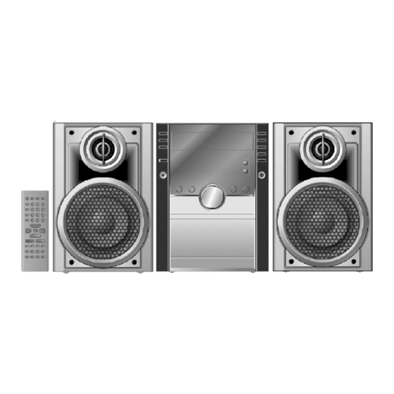
SA-AK250PL
Colour
(S)... Silver Type
Terminal
Sensitivity
Phone jack
Terminal
n CASSETTE DECK SECTION
Track system
Heads
Record/playback
Erasure
Motor
Recording system
Erasing system
Tape speed
Overall frequency response (+3, -6 dB) at DECK OUT
NORMAL
S/N ratio
Wow and flutter
Fast forward and rewind time
n DISC SECTION
Disc played [8 cm or 12 cm]
(1) CD-Audio (CD-DA)
(2) CD-R/RW (CD-DA, MP3* formatted disc)
© 2007 Matsushita Electric Industrial Co. Ltd.. All
rights
reserved.
distribution is a violation of law.
ORDER NO. MD0704054CE
CD Stereo System
Stereo, 3.5 mm jack
100 mV, 4.7 kΩ
Stereo, 3.5 mm jack
4 track, 2 channel
Solid permalloy head
Double gap ferrite head
DC servo motor
AC bias 100 kHz
AC erase 100 kHz
35 Hz to 14 kHz
50 dB (A weighted)
0.18 % (WRMS)
Approx. 120 seconds with
C-60 cassette tape
Unauthorized
copying
4.8 cm/s
and
Advertisement
Table of Contents

Related Manuals for Panasonic SA-AK250PL


Summary of Contents for Panasonic SA-AK250PL
-
Page 1: Specifications
ORDER NO. MD0704054CE CD Stereo System SA-AK250PL Colour (S)... Silver Type Notes: This model’s CD mechanism changer unit is CRS1. Please refer to the original Service Manual (Order No. MD0509368C0) for this mechanism. Specifications RMS output power Terminal Stereo, 3.5 mm jack... -
Page 2: Table Of Contents
SA-AK250PL (3) MP3* Power consumption 100 W *MPEG-1 Layer 3, MPEG-2 Layer 3 Power consumption in standby 0.28 W mode Bit rate Dimensions (W x H x D) 250 x 330 x 323 mm 32 kbps to 320 kbps Mass 7.1 kg... - Page 3 SA-AK250PL 15.1. CD Servo P.C.B. 19.6. (F) Deck Circuit 15.2. Deck P.C.B. & Deck Mechanism P.C.B. 19.7. (H) Transformer Circuit 15.3. Main P.C.B. 20 Printed Circuit Board 15.4. Panel P.C.B. & Transformer P.C.B. 20.1. (A) CD Servo P.C.B., (F) Deck P.C.B. & (G) Deck 15.5.
-
Page 4: Safety Precautions
SA-AK250PL 1 Safety Precautions 1.1. General Guidelines 1. When servicing, observe the original lead dress. If a short circuit is found, replace all parts which have been overheated or damaged by the short circuit. 2. After servicing, ensure that all the protective devices such as insulation barriers and insulation papers shields are properly installed. -
Page 5: Protection Circuitry
SA-AK250PL 1.3. Protection Circuitry The protection circuitry may have operated if either of the following conditions are noticed: · No sound is heard when the power is turned on. · Sound stops during a performance. The function of this circuitry is to prevent circuitry damage if, for example, the positive and negative speaker connection wires are “shorted”, or if speaker systems with an impedance less than the indicated rated impedance of the amplifier are used. - Page 6 SA-AK250PL 7. Immediately before removing the protective material from the leads of a replacement ES device, touch the protective material to the chassis or circuit assembly into which the device will be installed. Caution Be sure no power is applied to the chassis or circuit, and observe all other safety precautions.
-
Page 7: Handling Precautions For Traverse Unit
SA-AK250PL 3 Handling Precautions For Traverse Unit The laser diode in the traverse unit (with optical pickup) may break down due to potential difference caused by the static electricity of clothes or our human body. So, be careful of electrostatic breakdown during repair of the traverse unit (with optical pickup). - Page 8 SA-AK250PL...
-
Page 9: Precaution Of Laser Diode
SA-AK250PL 4 Precaution of laser diode CAUTION: This unit utilizes a class 1 laser diode in the optical pickup unit . Invisible laser radiation is emitted from the optical pickup lens. Wavelength: 780nm When the unit is turned on: 1. Do not look directly into the optical pickup lens. -
Page 10: About Lead Free Solder (Pbf)
SA-AK250PL 5 About Lead Free Solder (PbF) 5.1. Service caution based on legal restrictions 5.1.1. General description about Lead Free Solder (PbF) The lead free solder has been used in the mounting process of all electrical components on the printed circuit boards used for this equipment in considering the globally environmental conservation. -
Page 11: Accessories
SA-AK250PL 6 Accessories Note: Refer to “Replacement Parts List” (Section 24) for part number. Remote Control FM Antenna Wire AC Cord AM Loop Antenna... -
Page 12: Operating Procedures
SA-AK250PL 7 Operating Procedures 7.1. Main Unit Key Buttons Operations... -
Page 13: Remote Control Key Buttons Operations
SA-AK250PL 7.2. Remote Control Key Buttons Operations... -
Page 14: New Features
SA-AK250PL 8 New Features 8.1. Using the Music Port This feature enables you to enjoy music from a portable audio equipment. - Page 15 SA-AK250PL With reference to page 15 of the operating instruction manual.
-
Page 16: Self Diagnosis And Special Mode Setting
SA-AK250PL 9 Self diagnosis and special mode setting This unit is equipped with functions for checking and inspecting namely: Self-Diagnostic and Test Mode. 9.1. Service Mode Summary Table The service modes can be activated by pressing various button combination on the main unit and remote control unit. Below is the... - Page 17 SA-AK250PL...
- Page 18 SA-AK250PL 9.2.1. EEPROM Checksum (ROM Correction) Purpose: To check for microprocessor firmware version and EEPROM checksum (ROM correction).
-
Page 19: Reliability Test Mode (Crs1 Mechanism)
SA-AK250PL Below are the procedures for this mode. Step 1: Enter into Doctor mode (for more information, refer to section 9.2 on the key operation to enter into this mode. Step 2: Check for firmware version and EEPROM checksum (By pressing STOP button on main unit followed by “4” and “7” on remote control). - Page 20 SA-AK250PL...
-
Page 21: Error Code Table Display
SA-AK250PL 9.4. Error code Table Display Self-Diagnosis Function (refer Section 9.2) provides information on any problems occuring for the unit and its respective components by displaying the error codes. These error code such as U**, H** and F** are stored in memory and held unless it is cleared. - Page 22 SA-AK250PL 9.4.2. Error Code Table For CD Changer Block...
- Page 23 SA-AK250PL...
- Page 24 SA-AK250PL...
- Page 25 SA-AK250PL 9.4.3. Error Code Table For Power Supply 9.4.4. CRS1 Error Code display CRS1 Error Code display 1. The errors that occured in CRS1 Mechanism can be recalled and displayed, in the order of the occurence under self-diagnostic for procedures to enter this mode.
-
Page 26: Assembling And Disassembling
SA-AK250PL 10 Assembling and Disassembling 10.1. Caution Special Note: This model uses a new CD changer unit CRS1. In this following section does not contain the necessary disassembly & assembly information for the CD changer unit (CRS1) except the disasembly & assembly of traverse unit. Kindly refer to the original service manual for the CD changer unit. -
Page 27: Disassembly Flow Chart
SA-AK250PL 10.2. Disassembly flow chart The following chart is the procedure for disassembling the casing and inside parts for internal inspection when carrying out the servicing. To assemble the unit, reverse the steps shown in the chart as below. -
Page 28: Main Parts Location
SA-AK250PL 10.3. Main Parts Location... -
Page 29: Disassembly Of Top Cabinet
SA-AK250PL 10.4. Disassembly of Top Cabinet Step 1 Remove 3 screws on both sides on top cabinet. Step 2 Remove 5 screws at the rear. Step 3 Lift the sides of top cabinet outwards. Step 4 Push the top cabinet backwards to release catches. -
Page 30: Disassembly Of Rear Panel
SA-AK250PL · Disassembly of Mecha Chassis Step 5 Remove 2 screws. Step 6 Remove the Mecha Chassis. Note: For disassembly & assembly of traverse unit, please refer to section 10.15 of this service manual. Please refer to original Service Manual for the Disassembly and Assembly of the CD Changer Unit (CRS1). -
Page 31: Disassembly Of Main P.c.b
SA-AK250PL 10.7. Disassembly of Main P.C.B. · Follow the (Step 1) - (Step 5) of Item 10.4 · Follow the (Step 1) - (Step 4) of Item 10.5 · Follow the (Step 1) - (Step 4) of Item 10.6 Step 1 Detach FFC cables at connectors (CN2803 & CN2806) on Main P.C.B.. -
Page 32: Disassembly Of Power P.c.b
SA-AK250PL 10.9. Disassembly of Power P.C.B. · Follow the (Step 1) - (Step 5) of Item 10.4 · Follow the (Step 1) - (Step 4) of Item 10.5 · Follow the (Step 1) - (Step 4) of Item 10.6 · Follow the (Step 1) - (Step 3) of Item 10.7 Step 1 Flip the Power P.C.B. -
Page 33: Disassembly For Panel P.c.b
SA-AK250PL Step 4 Release 2 claws outwards. Step 3 Bent the front panel unit slightly forward as arrow shown. Step 5 Remove the front panel unit. Note: Ensure 2 claws located at the bottom chassis is seated into the 2 slots at bottom of front panel at 2 catches (one on each side) of bottom chassis to be aligned to front panel’s slot. -
Page 34: Disassembly Of Tact Switch P.c.b
SA-AK250PL Step 2 Remove Lid. Note: Do not misplace the spring. 10.12. Disassembly of Tact Switch P.C.B. · Follow the (Step 1) - (Step 5) of Item 10.4 · Follow the (Step 1) - (Step 4) of Item 10.5 · Follow the (Step 1) - (Step 5) of Item 10.10 Step 1 Remove 6 screws at Tact Switch P.C.B.. -
Page 35: Disassembly Of Traverse Unit
SA-AK250PL Step 1 Remove 2 screws. Step 2 Desolder wire at deck motor terminals. Step 3 Remove Deck P.C.B. 10.15. Disassembly of Traverse Unit · Follow the (Step 1) - (Step 5) of Item 10.4 · Follow the (Step 1) - (Step 4) of Item 10.5 Important notes: Ensure all the trays are in the “STOCK”... -
Page 36: Disassembly For Deck Mechanism
SA-AK250PL Step 3: Remove the traverse unit as arrow shown. · Assembly of Traverse Unit Step 2: Push the traverse slide plate as arrow shown to lock the traverse unit. Step 1: Turn over the unit and install the traverse unit. - Page 37 SA-AK250PL 10.16.1. Replacement of Pinch Roller and Head Block...
- Page 38 SA-AK250PL 10.16.2. Replacement of Motor, Capstan Belt A, Capstan Belt B, and Winding Belt...
-
Page 39: Disassembly Of Deck Mechanism P.c.b
SA-AK250PL 10.17. Disassembly of Deck Mechanism P.C.B. · Follow the (Step 1) - (Step 4) of Item 10.4 · Follow the (Step 1) - (Step 4) of Item 10.5 · Follow the (Step 1) - (Step 5) of Item 10.10 ·... -
Page 40: Disassembly Of Cassette Lid
SA-AK250PL 10.18. Disassembly of cassette lid · Follow the (Step 1) - (Step 4) of Item 10.4 · Follow the (Step 1) - (Step 4) of Item 10.5 · Follow the (Step 1) - (Step 5) of Item 10.10 · Follow the (Step 1) - (Step 3) of Item 10.13 Step 1 Open the cassette lid. - Page 41 SA-AK250PL Note: Follow 10.18 Disassembly of cassette lid (Step1) to (Step 3). Remove the cassette tape.
-
Page 42: Service Fixture And Tools
SA-AK250PL 11 Service Fixture and Tools Service Tools Extension FFC (A) Deck P.C.B. - Main P.C.B. REEX0485 (14 Pins) 12 Service Positions Note: For description of the disassembly procedures, see the Section 10. 12.1. Checking and Repairing of Main P.C.B. -
Page 43: Checking And Repairing Of Transformer P.c.b
SA-AK250PL 12.2. Checking and Repairing of Transformer P.C.B. 12.3. Checking and Repairing of Panel, Deck & Deck Mechanism P.C.B. -
Page 44: Checking And Repairing Of Power P.c.b
SA-AK250PL 12.4. Checking and Repairing of Power P.C.B. -
Page 45: Procedure For Checking Operation Of Individual Parts Of Deck Mechanism Unit
SA-AK250PL 13 Procedure for Checking Operation of Individual Parts of Deck Mechanism Unit 13.1. Operation Check with Cassette Tape 1. Pull up the EJECT lever using a rubber band. (Fig. 6) 2. Supply DC5V to MOTOR. (→ MOTOR rotates.) (Fig. 5) 3. - Page 46 SA-AK250PL...
-
Page 47: Measurement And Adjustments
SA-AK250PL 14 Measurement And Adjustments 14.1. Cassette Deck Section 14.1.1. Requirements · Test tape (QZZCFM) (QZZCWAT) · Normal blank cassette tape (QZZCRA) · Digital frequency counter · Oscilloscope · Electrical voltmeter · Headphone jack output jig (Fig 8) 14.1.2. Setting of Unit ·... - Page 48 SA-AK250PL Fig. 10 Fig. 11 14.1.5. Bias Voltage Check 1. Connect an electrical voltmeter. (Fig 12) (Fig 9 for location of test point) 2. Set the function to “TAPE” position. 3. Insert a normal blank cassette tape (QZZCRA). 4. While pressing and holding down [REC( )] button, press [TAPE( )] button to pause the recording mode.
-
Page 49: Voltage And Waveform Chart
SA-AK250PL 15 Voltage and Waveform Chart Note: Circuit voltage and waveform described herein shall be regarded as reference information when probing defect point, because it may differ from an actual measuring value due to difference of Measuring instrument and its measuring condition and product itself. -
Page 50: Main P.c.b
SA-AK250PL 15.3. Main P.C.B. -
Page 51: Panel P.c.b. & Transformer P.c.b
SA-AK250PL 15.4. Panel P.C.B. & Transformer P.C.B. 15.5. Power P.C.B. -
Page 52: Waveform Chart
SA-AK250PL 15.6. Waveform Chart... -
Page 53: Wiring Connection Diagram
SA-AK250PL 16 Wiring Connection Diagram JK2803 9 ..1 CN3601 H5104 CN2810 TUNER PACK MOTOR CN2809 POWER P.C.B. SOLDER SIDE CN2801 MAIN P.C.B. SOLDER SIDE RIGHT SPEAKER TO CRS1 JK5103 (CN1) LEFT SPEAKER CN2808 CN2805 CN5103 1 . - Page 54 SA-AK250PL...
-
Page 55: Block Diagram
SWITCH PROCESSOR/ TO MAIN CN7002 CN2801 (1/2) DIGITAL FILTER 3.3V 3.3V 3.3V 3.3V D/A CONVERTER MUTE PC1 4 CN7002 CN2801 [CH1] LCH OUT 3.3V TO MAIN CN7002 CN2801 (2/2) RCH OUT MUTE PC2 2 [CH2] SA-AK250PL CD SERVO BLOCK DIAGRAM... -
Page 56: Deck/ Deck Mechanism Diagram
SWITCH SWITCH SWITCH Q1312 Q1317 SWITCH SWITCH Q1316 Q1314 SWITCH SWITCH IC1000 C1AA00000612 ANALOG SWITCH DECK MECHANISM CIRCUIT TO MAIN (2/2) VREF D971 Q1315 IC971 CNB13030R2AU PHOTO INTERUPTOR SWITCH S971 MODE S972 HALF S975 RECINH_F SA-AK250PL DECK/DECK MECHANISM BLOCK DIAGRAM... -
Page 57: Main Diagram
MUTE 3.3V SWITCH SWITCH QR2501, QR2502 Q2511 MUTE SWITCH MUTEA SWITCH DRIVER ASPDA ASPCLK IDCDET Q2942 FAN MOTOR ON/OFF SWITCH TO FAN Q2943 FAN SUPPLY CONTROL SWITCH Q2949 Q2948 D2946 DC DETECT DC DETECT SWITCH SWITCH SA-AK250PL MAIN (1/2) DIAGRAM... - Page 58 IDCDET ASPDA ASPCLK Q2937 Q2936 VREF CD SUPPLY CHANGER PLUNGER ON/OFF SWITCH CONTROLSWITCH QR3105 QR3106 Q2803 SWITCH SWITCH IC4000 C0DBZGC00067 RESET (MICRO-P) 3.3 REGULATOR SWITCH Q3601 STBY SWITCH D2936 IC2872 C0CBAHG00011 VOLTAGE REGULATOR 3.3V D2811 D2813 SA-AK250PL MAIN (2/2) DIAGRAM...
-
Page 59: Panel Diagram
TO MAIN (2/2) Z6481 REMOTE SENSOR JK6751 TO MAIN MUSIC PORT (1/2) S6201-S6207 TO MAIN (2/2) JK6551 HEADPHONE TO MAIN (1/2) SUB PANEL CIRCUIT S6301-S6309 VR6491 +VREF MIC VOLUME +VREF TO MAIN (2/2) S6106,S6108 S6101-S6105 SUB PANEL P.C.B SA-AK250PL PANEL DIAGRAM... -
Page 60: Power Diagram
FAN ON/OFF SWITCH SWITCH D5126 TO MAIN (1/2) Q5111 Q5101,Q5110 +15V REGULATOR Q5102 Q5108,Q5109 CURRENT CONTROL SWITCH TO TRANSFORMER Q5112,Q5114 Q5113 CURRENT STABLISER CURRENT LMIITER 11V REGULATOR SWITCH IC5101 TO MAIN C0DAZYY00005 (2/2) REGULATOR IC D5130 5.6V 3.3V SA-AK250PL POWER DIAGRAM CTRL... -
Page 61: Transformer Diagram
: AM SIGNAL LINE : FM/AM/XM SIGNAL LINE : VIDOE SIGNAL LINE : FM SIGNAL LINE : AUX/IPOD SIGNAL LINE ) Indicates the Pin No. of Right Channel. NOTE : Signal Lines are applicable to the Left Channel only. SA-AK250PL TRANSFORMER DIAGRAM... - Page 62 SA-AK250PL...
-
Page 63: Notes Of Schematic Diagram
SA-AK250PL 18 Notes Of Schematic Diagram (All schematic diagrams may be modified at any time with : Main Signal line the development of new technology) : FM/AM Signal line Notes: S971: Mode switch. : Tape Record Signal line S972: Half switch. - Page 64 SA-AK250PL...
-
Page 65: Schematic Diagram
12 11 R7220 R7330 W7002 W7004 5.6K C7335 IC7002 X7201 C7315 H2B169500005 0.47 BA5948FPE2 C7334 4 CH DRIVE IC C7338 10V220 0.056 R7331 R7323 3.3k R7315 R7325 3.3k R7332 R7335 M7301 M7302 TRAVERSE MOTOR SPINDLE MOTOR SA-AK250PL CD SERVO CIRCUIT... -
Page 66: B) Main Circuit
SA-AK250PL 19.2. (B) Main Circuit SCHEMATIC DIAGRAM - 2 MAIN CIRCUIT : +B SIGNAL LINE : CD SIGNAL : TAPE RECORD SIGNAL LINE : TAPE PLAYBACK SIGNAL LINE : FM/AM SIGNAL LINE : MAIN SIGNAL LINE : AUX SIGNAL LINE... -
Page 67: Main Circuit
C2325 R2329 C2321 R2321 50V1 LOW_L-IN IN SCHEMATIC R2326 R2356 DIAGRAM-9 LOW_R-IN 180k C2329 A_GND 4700P SUBW C2330 R2456 W586 180k 0.22 R2417 R2418 100k Q2417 R2416 2.2k C2943 50V2.2 W673 W654 TO MAIN SECTION (4/4) W757 SA-AK250PL MAIN CIRCUIT... - Page 68 SA-AK250PL SCHEMATIC DIAGRAM - 4 MAIN CIRCUIT : +B SIGNAL LINE : CD SIGNAL LINE : FM/AM SIGNAL LINE : MAIN SIGNAL LINE : AUX SIGNAL LINE R2284 W658 W617 R2285 D2811 B0ADCJ000020 R2894 R2121 3.3k TO MAIN SECTION (1/4)
- Page 69 Q2937 D2937 Q2936 28 27 25 24 21 20 12 11 11 12 13 14 B1ACKD000006 CD SUPPLY CONTROL SWITCH Q2937 B1GBCFJJ0051 CHANGER PLUNGER CN2806 CN2805 ON/OFF SWITCH TO CRSI (CN1) PANEL CIRCUIT (CN6601) IN SCHEMATIC DIAGRAM-6 SA-AK250PL MAIN CIRCUIT...
-
Page 70: C) Panel Circuit
W1000 KEY1 IN W913 3 2 1 C6623 HP_SW W903 W1004 50V22 GND2 Z6481 W915 B3RAD0000146 JK6551 W910 W1006 REMOTE SENSOR W1003 W1005 R6763 W1001 W1002 R6753 R6751 3.3K 3.3K MUSIC PORT C6753 C6751 0.01 0.01 JK6751 SA-AK250PL PANEL CIRCUIT... -
Page 71: D) Sub Panel Circuit & (G) Deck Mechanism Circuit
2.2K R6491 R6107 2.7K S6306 S6108 R6307 2.7K C6492 C6491 M.EQ + 100P 100P HARD BASS R6108 4.7K S6307 R6308 R6310 MANUAL 4.7K COM B S6308 R6309 6.8K M.EQ - S6309 VR6491 EVEKE2F3024B VOLUME JOG SA-AK250PL SUB PANEL/DECK MECHANISM CIRCUIT... -
Page 72: E) Power Circuit
IC5201 B1ABCF000176 Q5103,Q5104 0.47 Q5201 X5202 B1ABCF000176 FREQUENCY HOPPING SWITCH H2A375300003 FAN ON/OFF SWITCH R5207 Q5202 Q5104 6.8K B1ADCF000176 Q5202 Q5103 FREQUENCY HOPPING X5201 SWITCH H2A415300001 R5209 C5204 100P C5205 C5208 6.3V220 AGND D5126 R5150 B0ACCK000005 220K SA-AK250PL POWER CIRCUIT... - Page 73 R5134 R5105 IN SCHEMATIC R5110 MUTE_F 1.2K 2.2K mUTE-F_HOP C5133 DIAGRAM-5 MOTOR12V 6.3V100 D5103 C5113 D5109 MOTOR 12V B0BA5R000004 R5132 50V33 B0BA01100004 XM5.3V AGND W744 Q5109 Q5114 +3.3V 2SB0709AHL CN5103 B1ABCF000176 VOLTAGE REGULATOR 11V REGULATOR E5103 K9ZZ00001279 SA-AK250PL POWER CIRCUIT...
-
Page 74: F) Deck Circuit
R1337 R1332 B0ACCK000005 MOTOR_GND MOTOR_H C1311 C1320 16V47 50V1 R1331 DECK MECHANISM (CS971) Q1315 CN1305 7.5K ON SCHEMATIC DIAGRAM-7 Q1314 R1344 R1342 R1341 R1374 R1343 3.3K Q1316 WR1903 R1345 2SD09650RA SWITCH Q1314 Q1315 B1GDCFGH0002 B1ACKD000006 SWITCH SWITCH SA-AK250PL DECK CIRCUIT... -
Page 75: H) Transformer Circuit
Q5953 L5950 ELF15N035AN C5951 JK5950 DGND 0.01u C5953 AC IN 0.01u 120V 60Hz R5952 Z5950 125V 3.15A 4.7K ERZV10V511CS R5958 C5963 R5953 Q5953 B1AACF000064 Q5952 B1GACFJJ0018 PCONT SWITCH C5962 C5952 SYNCHRONISATION SWITCH 10V220 C5954 R5957 10V47 0.01 SA-AK250PL TRANSFORMER CIRCUIT... - Page 76 SA-AK250PL...
-
Page 77: Printed Circuit Board
SA-AK250PL 20 Printed Circuit Board Note: Circuit board diagrams may be modified at any time with the development of new technology. -
Page 78: A) Cd Servo P.c.b., (F) Deck P.c.b. & (G) Deck
SA-AK250PL 20.1. (A) CD Servo P.C.B., (F) Deck P.C.B. & (G) Deck Mechanism P.C.B. CD SERVO P.C.B (REPV0111A) DECK P.C.B (REPV0134B) (RF) TP51 C7227 W1930 W7014 Q1309 CN1305 Q1310 C7204 W7015 W1909 W1935 C7226 R7212 TP18 TP50 C7228 C1317 TP17... -
Page 79: B) Main P.c.b
SA-AK250PL 20.2. (B) Main P.C.B. MAIN P.C.B (REPV0130M) W565 L2996 R2447 C2705 R2702 R2941 R2446 C2941 C2312 C2240 Q2441 R2705 R2703 W277 R2241 C2983 W569 R2944 C2981 R2315 C2703 C2944 C2441 Q2943 C2314 C2313 C2341 JK2803 R2353 R2344 R2347 W642... -
Page 80: C) Panel P.c.b
SA-AK250PL 20.3. (C) Panel P.C.B. PANEL P.C.B (REPV0131L) S6201 S6103 (CD1) (OPEN/CLOSE) S6202 S6102 (CD2) (MULTI CHANGE) W805 R6632 S6203 R6105 (CD3) J6553 J6551 S6104 (SINGLE CHANGE) S6204 R6458 (CD4) W840 R6199 J6552 R6209 W1017 J6753 R6208 S6206 R6206 (/FF/) -
Page 81: D) Sub Panel P.c.b
SA-AK250PL 20.4. (D) Sub Panel P.C.B. SUB PANEL P.C.B (REPV0131L) JW6001 S6304 S6305 (TUNER/ R6302 R6303 FM/AM) (EXT_IN) VR6491 R6304 S6302 S6303 (CD) (TAPE) W960 W750 W968 R6305 C6491 C6492 W971 W756 R6492 R6108 W958 R6307 S6108 S6106 S6301 S6307... -
Page 82: E) Power P.c.b
SA-AK250PL 20.5. (E) Power P.C.B. POWER P.C.B (REPV0133D) H5104 W701 C5171 W602 W714 C5102 C5103 C5172 R5203 W662 W697 R5201 W698 R5202 Q5202 C5204 W700 C5203 W691 C5202 W737 W638 R5207 Q5201 C5301 C5302 R5522 C5332 C5330 R5206 W639 R5302... -
Page 83: H) Transformer P.c.b
SA-AK250PL 20.6. (H) Transformer P.C.B. TRANSFORMER P.C.B (REPV0132J) T5951 125V 3.15A (SUB TRANSFORMER) L5950 C5953 Q5950 J5955 R5952 Z5950 C5951 C5952 D5952 RL5950 C5954 JK5950 Q5952 W5914 Q5953 W5915 CN5951 R5958 AC IN ~ W5905 R5951 R5960 120V 60HZ R5961... - Page 84 SA-AK250PL...
-
Page 85: Illustration Of Ics, Transistors And Diodes
SA-AK250PL 21 Illustration of ICs, Transistors and Diodes C0AABB000125 C0CBAHG00011 C1AA00000612 C0DBZGC00067 C1BB00001121 (100P) MN6627954MA (100P) C0HBB0000057 (44P) C2CBYY000482 (100P) CNB13030R2AU C0DAZYY00005 C1BA00000487 (24P) AN7326K (26P) BA5948FPE2 B1DEGM000026 C0JBAB000011(14P) B1ADCF000001 2SB0709AHL B1BACG000023 B1AAGC000006 B1GACFJJ0018 2SD09650RA B1GDCFJJ0047 B1ABGC000005 B1BCCG000002 B1ADCF000063 B1GBCFJJ0051... -
Page 86: Terminal Function Of Ic's
SA-AK250PL 22 Terminal Function of IC's 22.1. IC7001 (MN6627954MA) Servo Processor,Digital Signal Processor/Digital filter and D/A Converter Pin No. Mark Function Pin No. Mark Function DRAM address signal O/P 11 DSLF Loop Filter Terminal (For DSL) DRAM address signal O/P 9... -
Page 87: Ic7002 (Ba5948Fpe2) Ic 4Ch Drive
SA-AK250PL 22.2. IC7002 (BA5948FPE2) IC 4CH Drive Pin No. Mark Function Pin No. Mark Function Motor Driver 92 Input Motor Drive (3) reverse - action output Turntable Motor Drive Signal (“L”:ON) Motor Drive (3) forward - action output Motor Drive (1) Input... - Page 88 SA-AK250PL Pin No. Mark Function MCLK CD Command Clock Output /RESET_SW CD Limit Switch Input for the most Inner Point (Active Low) HOME_SW Home Switch for CRS1 CD_RST CD Reset output CLOSE_SW CLOSE switch for CRS1 OPEN_SW Open switch for CRS1...
-
Page 89: Exploded Views
SA-AK250PL 23 Exploded Views 23.1. Cabinet Parts Location... - Page 90 SA-AK250PL...
-
Page 91: Deck Mechanism Parts Location (Raa4403-S)
SA-AK250PL 23.2. Deck Mechanism Parts Location (RAA4403-S) -
Page 92: Packaging
SA-AK250PL 23.3. Packaging... -
Page 93: Replacement Parts List
SA-AK250PL 24 Replacement Parts List Notes: · Important safety notice: Components identified by mark have special characteristics important for safety. Furthermore, special parts which have purposes of fire-retardent (resistors), high-quality sound (capacitors), low noise (resistors), etc are used. When replacing any of these components, be sure to use only manufacturer’s specified parts shown in the parts list. - Page 94 SA-AK250PL Ref. No. Part No. Part Name & Description Remarks Ref. No. Part No. Part Name & Description Remarks REM0120 CAP MOTOR ASS’Y Q2949 B1ABCF000176 TRANSISTOR RHD26022-1 MOTOR SCREW Q3601 2SC3940A0A TRANSISTOR XTW2+5LFJ H/BLOKC UNIT SCREW Q5101 B1DEGM000026 TRANSISTOR XTW26+10SFJ...
- Page 95 SA-AK250PL Ref. No. Part No. Part Name & Description Remarks Ref. No. Part No. Part Name & Description Remarks D5954 B0EAKP000134 DIODE D5955 B0EAKP000134 DIODE CS971 RJU071H09M1 9P CONNECTOR D5956 B0EAKP000134 DIODE D5957 B0EAKP000134 DIODE COILS & TRANSFORMERS D5958 B0EAKP000134...
- Page 96 SA-AK250PL Ref. No. Part No. Part Name & Description Remarks Ref. No. Part No. Part Name & Description Remarks W645 ERJ6GEY0R00V CHIP JUMPER E5101 K9ZZ00001279 EARTH PLATE W646 ERJ6GEY0R00V CHIP JUMPER E5103 K9ZZ00001279 EARTH PLATE W647 ERJ6GEY0R00V CHIP JUMPER W648...
- Page 97 SA-AK250PL Ref. No. Part No. Part Name & Description Remarks Ref. No. Part No. Part Name & Description Remarks W1012 ERJ8GEY0R00V CHIP JUMPER R1203 D0GB183JA008 18K 1/16W W7001 D0GDR00JA017 CHIP JUMPER R1204 D0GB103JA008 10K 1/16W W7002 D0GDR00JA017 CHIP JUMPER R1205 D0GB222JA007 2.2K 1/16W...
- Page 98 SA-AK250PL Ref. No. Part No. Part Name & Description Remarks Ref. No. Part No. Part Name & Description Remarks R2248 D0GB682JA008 6.8K 1/16W R2676 D0GBR00JA008 0 1/16W R2249 D0GB332JA007 3.3K 1/16W R2677 ERJ6GEYJ271V 270 1/10W R2251 D0GBR00JA008 0 1/16W R2701...
- Page 99 SA-AK250PL Ref. No. Part No. Part Name & Description Remarks Ref. No. Part No. Part Name & Description Remarks R2948 D0GB101JA007 100 1/16W R5953 D0AE151JA048 150 1/4W R2949 D0GB473JA041 47K 1/16W R5957 D0AE103JA048 10K 1/4W R3210 D0GB104JA007 100K 1/16W R5958...
- Page 100 SA-AK250PL Ref. No. Part No. Part Name & Description Remarks Ref. No. Part No. Part Name & Description Remarks R7601 ERJ3GEYJ4R7V 4.7 1/16W C2183 ECJ1VB1C224K 0.22 16V R7650 ERJ3GEYJ5R6V 5.6 1/16W C2191 F2A1H3R3A234 3.3 50V C2192 F1H1C104A041 0.1 16V K3300...
- Page 101 SA-AK250PL Ref. No. Part No. Part Name & Description Remarks Ref. No. Part No. Part Name & Description Remarks C2753 F1H1C104A042 0.1 16V C5301 ECJ1VB1A474K 0.47 10V C2802 F2A1H3R3A234 3.3 50V C5302 F1H1H331A013 330P 50V C2803 F1H1A105A025 1 10V C5303 ECJ1VB1A474K 0.47 10V...
- Page 102 SA-AK250PL Ref. No. Part No. Part Name & Description Remarks C6752 F1H1H103A219 0.01 50V C6753 F1H1H103A219 0.01 50V C7102 F1H1A474A025 0.47 10V C7107 ECJ1VB1H223K 0.022 50V C7142 ECJ1VB1H332K 3300P 50V C7154 ECJ1VB1C104K 0.1 16V C7155 ECJ1VB1C104K 0.1 16V C7161 ECJ1VB1C104K 0.1 16V...
Need help?
Do you have a question about the SA-AK250PL and is the answer not in the manual?
Questions and answers