Table of Contents
Advertisement
Quick Links
Advertisement
Table of Contents

Related Manuals for Clevo x7200


Summary of Contents for Clevo x7200
- Page 3 Preface Notebook Computer X7200 Service Manual...
- Page 4 Preface Notice The company reserves the right to revise this publication or to change its contents without notice. Information contained herein is for reference only and does not constitute a commitment on the part of the manufacturer or any subsequent ven- dor.
- Page 5 This manual is intended for service personnel who have completed sufficient training to undertake the maintenance and inspection of personal computers. It is organized to allow you to look up basic information for servicing and/or upgrading components of the X7200 series notebook PC.
- Page 6 Preface IMPORTANT SAFETY INSTRUCTIONS Follow basic safety precautions, including those listed below, to reduce the risk of fire, electric shock and injury to per- sons when using any electrical equipment: 1. Do not use this product near water, for example near a bath tub, wash bowl, kitchen sink or laundry tub, in a wet basement or near a swimming pool.
-
Page 7: Instructions For Care And Operation
Preface Instructions for Care and Operation The notebook computer is quite rugged, but it can be damaged. To prevent this, follow these suggestions: Don’t drop it, or expose it to shock. If the computer falls, the case and the components could be damaged. Do not expose the computer Do not place it on an unstable Do not place anything heavy... -
Page 8: Power Safety
Preface Avoid interference. Keep the computer away from high capacity transformers, electric motors, and other strong mag- netic fields. These can hinder proper performance and damage your data. Take care when using peripheral devices. Use only approved brands of Unplug the power cord before peripherals. -
Page 9: Battery Precautions
Preface Battery Precautions • Only use batteries designed for this computer. The wrong battery type may explode, leak or damage the computer. • Do not continue to use a battery that has been dropped, or that appears damaged (e.g. bent or twisted) in any way. Even if the computer continues to work with a damaged battery in place, it may cause circuit damage, which may possibly result in fire. -
Page 10: Related Documents
Preface Related Documents You may also need to consult the following manual for additional information: User’s Manual on CD/DVD This describes the notebook PC’s features and the procedures for operating the computer and its ROM-based setup pro- gram. It also describes the installation and operation of the utility programs provided with the notebook PC. System Startup 1. -
Page 11: Table Of Contents
Preface Contents Introduction ..........1-1 Part Lists ..........A-1 Overview ..................1-1 Part List Illustration Location ............A-2 Specifications ..................1-2 Top ....................A-3 External Locator - Top View with LCD Panel Open ......1-4 Bottom ................... A-4 External Locator - Front & Right Side Views .........1-5 LCD .................... - Page 12 Preface Clock Buffer ICS9DB403GLFT ..........B-21 Power LED Board .................B-53 MXM 3.0 PCI-E Master ............... B-22 Updating the FLASH ROM BIOS..C-1 MXM 3.0 PCI-E SLAVER ............B-23 To update the FLASH ROM BIOS you must: C-1 HDMI-In Buffer/SATA HDD CON ..........B-24 Download the BIOS ................C-1 HDMI Port ..................
-
Page 13: Introduction
Chapter 1: Introduction Overview This manual covers the information you need to service or upgrade the X7200 series notebook computer. Information about operating the computer (e.g. getting started, and the Setup utility) is in the User’s Manual. Information about dri- vers (e.g. -
Page 14: Specifications
Introduction Specifications Processor Options Video Adapter Intel® Core™ i7 Processor nVIDIA® GeForce GTX 480M / GTX 485M / GTX 470M / GTX 460M / N10E-GLM3 PCIe Video Card (SLI) i7-975 (3.33 GHz, 6.4 GT/s, 8M L3 Cache, 45nm, LGA1366 Package) 2GB GDDR5 Video RAM on board ... - Page 15 Introduction Card Reader High Definition Audio Compliant Interface S/PDIF Digital Output Embedded 9-in-1 Card Reader Five Speakers MMC (MultiMedia Card) / RS MMC One Sub Woofer SD (Secure Digital) / Mini SD / SDHC/ SDXC Compatible Built-In Microphone MS (Memory Stick) / MS Pro / MS Duo Dolby Home Theater (5.1 Channel) Certified Mini Card Slots External 7.1 Chanel for Power DVD and Gaming...
-
Page 16: External Locator - Top View With Lcd Panel Open
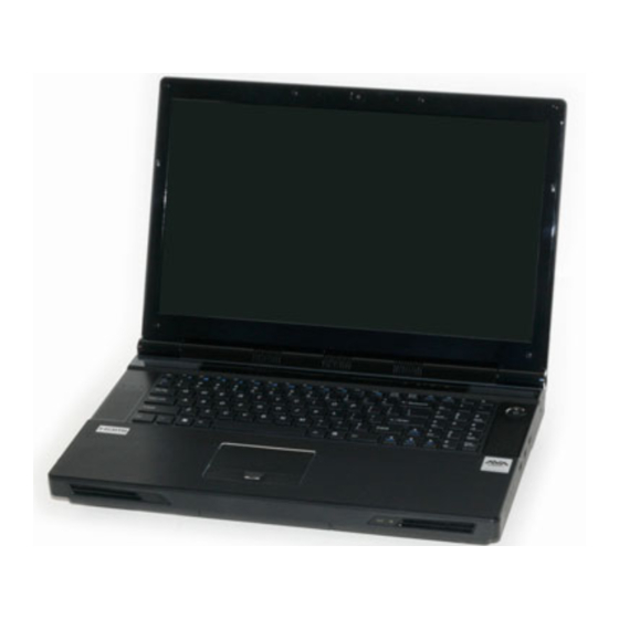
Introduction External Locator - Top View with LCD Panel Open Figure 1 Top View 1. PC Camera 2. Built-In Digital Microphone 3. LCD 4. LED Status Indicators 5. Touch Sensor Instant Keys 6. Speakers 7. Power Button 8. Keyboard 9. TouchPad and Buttons 10.Fingerprint Reader Module... -
Page 17: External Locator - Front & Right Side Views
Introduction External Locator - Front & Right Side Views Figure 2 Front View 1. Infrared Receiver 2. LED Power Indicators FRONT VIEW Figure 3 Right Side View 1. Line-In Jack RIGHT SIDE VIEW 2. S/PDIF-Out Jack 3. Microphone-In Jack 4. Headphone-In Jack 5. -
Page 18: External Locator - Left Side & Rear View
Introduction External Locator - Left Side & Rear View Figure 4 Left Side View 1. DVI-Out Port 2. Cable (CATV) Antenna Jack 3. RJ-45 LAN Jack LEFT SIDE VIEW 4. HDMI-Out Port 5. USB 3.0 Ports 6. eSATA Port 7. Mini-IEEE 1394b Port 8. -
Page 19: External Locator - Bottom View
Introduction External Locator - Bottom View Figure 6 Bottom View 1. Component Bay Cover 2. Vent 3. Sub Woofer 4. Primary HDD Bay (HDD1 & 2) 5. Battery (Secondary HDD Bay - HDD3) Overheating To prevent your com- puter from overhea- ting, make sure no- thing blocks any vent while the computer is... -
Page 20: Mainboard Overview - Top (Key Parts)
Introduction Mainboard Overview - Top (Key Parts) Figure 7 Mainboard Top Key Parts 1. TV Turbo Me- mory Connector 2. Mini-Card Con- nector (WLAN Module) 3. KBC-ITE IT8502E 4. Memory Slots DDR3 SO-DIMM 5. Azalia Codec 1 - 8 Mainboard Overview - Top (Key Parts) -
Page 21: Mainboard Overview - Bottom (Key Parts)
Introduction Mainboard Overview - Bottom (Key Parts) Figure 8 Mainboard Bottom Key Parts 1. CPU Socket (no CPU installed) 2. VGA-Card Connectors 3. Clock Generator Mainboard Overview - Bottom (Key Parts) 1 - 9... -
Page 22: Mainboard Overview - Top (Connectors)
Introduction Mainboard Overview - Top (Connectors) Figure 9 Mainboard Top Connectors 1. HDMI-Out Port 2. USB 3.0 Ports 3. eSATA Port 4. Mini-IEEE 1394b Port 5. HDMI-In Port 6. Consumer Infrared Connector 7. Bluetooth Cable Connector 1 8. TouchPad Cable Connector 9. -
Page 23: Mainboard Overview - Bottom (Connectors)
Introduction Mainboard Overview - Bottom (Connectors) Figure 10 Mainboard Bottom Connectors 1. CPU Fan Cable Connector 1 2. CPU Fan Cable Connector 2 3. SATA HDD 2 Connector 4. VGA Fan 2 Cable Connector 5. VGA Fan 1 Cable Connector 6. - Page 24 Introduction 1 - 12...
-
Page 25: Disassembly
Chapter 2: Disassembly Overview This chapter provides step-by-step instructions for disassembling the X7200 series notebook’s parts and subsystems. When it comes to reassembly, reverse the procedures (unless otherwise indicated). We suggest you completely review any procedure before you take the computer apart. -
Page 26: Maintenance Tools
Disassembly NOTE: All disassembly procedures assume that the system is turned OFF, and disconnected from any power supply (the battery is removed too). Maintenance Tools The following tools are recommended when working on the notebook PC: • M3 Philips-head screwdriver •... -
Page 27: Maintenance Precautions
Disassembly Maintenance Precautions The following precautions are a reminder. To avoid personal injury or damage to the computer while performing a re- moval and/or replacement job, take the following precautions: Power Safety Warning 1. Don't drop it. Perform your repairs and/or upgrades on a stable surface. If the computer falls, the case and other Before you undertake components could be damaged. -
Page 28: Disassembly Steps
Disassembly Disassembly Steps The following table lists the disassembly steps, and on which page to find the related information. PLEASE PERFORM THE DISASSEMBLY STEPS IN THE ORDER INDICATED. To remove the Battery: To remove the Bluetooth Module: 1. Remove the battery page 2 - 5 1. -
Page 29: Removing The Battery
Disassembly Removing the Battery Figure 1 1. Turn the computer off, and turn it over. Battery Removal 2. Loosen screws (Figure 1a and carefully lift the battery (Figure 1b 3. Remove the battery from the battery bay (Figure 1c a. Loosen screws. b. -
Page 30: Removing The Optical (Cd/Dvd) Device
Disassembly Removing the Optical (CD/DVD) Device Figure 2 Optical Device 1. Turn off the computer, remove the battery (page 2 - Removal 2. Remove screws from the hard disk bay cover (Figure 2a & 3. Remove the hard disk bay cover (Figure 2b a. -
Page 31: Removing The Processor
Disassembly Removing the Processor Figure 3 Processor Removal 1. Turn off the computer, remove the battery (page 2 - 2. Remove the screws from the component bay cover (Figure 3a). a. Remove the screws from 3. Remove the screws from the CPU fan (Figure 3b). - Page 32 Disassembly 6. Carefully lift up the heat sink off the computer by pulling the plastic strip (Figure 4e). Figure 4 7. Press down and hold the latch (with the latch held down you will be able to release it) (Figure 4f).
-
Page 33: Removing And Installing The Video Card
Disassembly Removing and Installing the Video Card Figure 5 Video Card Video Card Removal Procedure Removal Procedure Turn off the computer, turn it over and remove the battery ( page 2 - 5 ) and component cover ( page 2 - 7 Remove screws Figure 5 a. - Page 34 Disassembly The video cards will pop up. & Figure 6 & Disconnect the video ca cables and remove the video cards & Figure 6 Video Card Removal (cont’d) e. The video cards will pop up. f. Disconnect the video card cables and re- move the video cards.
- Page 35 Disassembly Installing a New Video Card Figure 7 Installing a New & Prepare to fit the video cards into the slot by holding it at about a 30° angle ( page 2 - 10 Video Card The card needs to be fully into the slot, and the video card and socket have a guide-key and pin which align to allow the card to fit securely ( Figure 7 g.
-
Page 36: Removing The Keyboard
Disassembly Figure 8 Removing the Keyboard Keyboard Removal 1. Turn off the computer and remove the battery (page 2 - 2. Remove screws from the bottom of the computer (Figure 8a). a. Remove screws from the 3. Turn the computer over, open the Lid/LCD, and carefully (a cable is connected to the underside of the LED cover bottom of the computer. -
Page 37: To Remove The Keyboard
Disassembly 5. Remove screws from the keyboard (Figure 9d). Figure 9 6. Carefully lift the keyboard up, being careful not to bend the keyboard ribbon cable . Disconnect the keyboard Keyboard Removal ribbon cable from the locking collar socket (Figure 9e). - Page 38 Disassembly 8. Remove screws from the keyboard shielding plate (Figure 10g). Figure 10 9. Lift the keyboard shielding plate up in the direction of the arrow (Figure 10h). Keyboard 10. Remove the keyboard shielding plate (Figure 10i). Removal (cont’d.) g. Remove screws from the keyboard...
- Page 39 Disassembly Keyboard Shielding Plate Insertion Figure 11 Keyboard 1. When re-inserting the keyboard shielding plate make sure you insert it by sliding it into position at an angle as Shielding Plate illustrated by arrow below, and press it down into position (Figure 11a).
-
Page 40: Removing The Wireless Lan Module
Disassembly Removing the Wireless LAN Module Figure 12 Wireless LAN 1. Turn off the computer, remove the battery (page 2 - 5) and the keyboard (page 2 - Module Removal 2. The Wireless LAN module will be visible at point (Figure 12a on the mainboard. -
Page 41: Removing The Bluetooth Module
Disassembly Removing the Bluetooth Module Figure 13 Bluetooth Module 1. Turn off the computer, remove the battery (page 2 - 5) and the keyboard (page 2 - Removal 2. The Bluetooth module will be visible at point Figure 13a 3. Remove screw Figure 13b The Bluetooth module 4. -
Page 42: Removing The System Memory (Ram)
Disassembly Removing the System Memory (RAM) Figure 14 RAM Module The computer has three memory sockets for 204 pin Small Outline Dual In-line Memory Modules (SO-DIMM) support- Removal ing DDR3 1066/1333MHz. The main memory can be expanded up to 12GB. The SO-DIMM modules supported are 1024MB, and 2048MB and DDRIII Modules. - Page 43 Disassembly 5. Pull the latches to release the second and third modules if necessary. 6. Insert a new module holding it at about a 30° angle and fit the connectors firmly into the memory slot. 7. The module’s pin alignment will allow it to only fit one way. Make sure the module is seated as far into the slot as it will go.
-
Page 44: Removing The Hard Disk(S) From The Primary Hdd Bay
Disassembly Removing the Hard Disk(s) from the Primary HDD Bay Figure 15 Removing the The hard disk drive can be taken out to accommodate other 2.5" serial (SATA) hard disk drives with a height of 9.5mm Hard Disk(s) from (h). Follow your operating system’s installation instructions, and install all necessary drivers and utilities (as outlined in the Primary HDD Chapter 4 of the User’s Manual) when setting up a new hard disk. - Page 45 Disassembly 6. Remove screws (Figure 16d). *The number and sequence of screws to be removed will depend on Figure 16 whether or not you have one or two hard disks installed in the case. Removing the Hard Disk(s) from the Primary HDD Bay (cont’d.) d.
- Page 46 Disassembly Inserting the Primary Hard Disk(s) Figure 17 Inserting the 1. Insert the HDD(s) into the HDD case as illustrated (Figure 17a). *Make sure the cable connectors are Primary Hard facing towards the gap at the rear of the case. Disk(s) 2.
-
Page 47: Removing The Hard Disk From The Secondary Hdd Bay
Disassembly 3. Firmly insert the HDD cable into the hard disk assembly in the direction of the arrow as indicated Figure 18 below (Figure 18c). Inserting the 4. Insert the HDD assembly into the bay by pushing it straight down (Figure 18d). - Page 48 Disassembly Remove screws from the hard disk assembly ( Figure 19 Figure 19 2. Grip the tab and slide the hard disk assembly in the direction of the arrow (Figure 19b). Removing the 3. Lift the hard disk assembly out of the compartment (Figure 19b).
- Page 49 Disassembly 7. Replace screws (page 2 - 23). Figure 20 8. Insert the HDD assembly into the bay by pushing it straight down (do not insert the assembly at an angle) and then Removing the slide it in the direction of the arrow to lock in place (Figure 20e).
-
Page 50: Removing The Hinges
Disassembly Figure 21 Removing the Hinges Hinge Removal 1. The whole LCD assembly is detached from the base of the computer. 2. Re-insert hinges & (Figure 21a) into the top case and raise the LCD to a 90° angle (Figure 21b) to adjust a. - Page 51 Disassembly 5. Remove hinges & (Figure 22d). Figure 22 Hinge Removal d. Remove the hinges. 8 & 9.Hinges Removing the Hinges 2 - 27...
- Page 52 Disassembly 2 - 28...
-
Page 53: Part Lists
Part Lists Appendix A:Part Lists This appendix breaks down the X7200 series notebook’s construction into a series of illustrations. The component part numbers are indicated in the tables opposite the drawings. Note: This section indicates the manufacturer’s part numbers. Your organization may use a different system, so be sure to cross-check any relevant documentation. -
Page 54: Part List Illustration Location
Part Lists Part List Illustration Location The following table indicates where to find the appropriate part list illustration. Table A - 1 Part List Illustration Part X7200 Location page A - 3 page A - 4 Bottom page A - 5... -
Page 55: Top
Part Lists Figure A - 1 非耐落 黑色 非耐落 凱碩 藍天 互億 Top A - 3... -
Page 56: Bottom
Part Lists Bottom Figure A - 2 Bottom 非耐落 A - 4 Bottom... -
Page 57: Lcd
Part Lists Figure A - 3 LCD A - 5... -
Page 58: Sata Dvd Super-Multi
Part Lists SATA DVD Super-Multi Figure A - 4 SATA DVD Super- Multi 非 耐 落 A - 6 SATA DVD Super-Multi... -
Page 59: Sata Blu-Ray Combo
Part Lists SATA Blu-Ray Combo Figure A - 5 SATA Blu-Ray Combo 非耐落 SATA Blu-Ray Combo A - 7... -
Page 60: Vga-Gtx1
Part Lists VGA-GTX1 Figure A - 6 VGA-GTX1 (半卡) (半卡) 非耐落 增加 A - 8 VGA-GTX1... - Page 61 Schematic Diagrams Appendix B: Schematic Diagrams This appendix has circuit diagrams of the X7200 notebook’s PCB’s. The following table indicates where to find the ap- propriate schematic diagram. Table B - 1 SCHEMATIC Diagram - Page Diagram - Page Diagram - Page...
-
Page 62: Schematic Diagrams
Schematic Diagrams System Block Diagram CLEVO X7200 System Block Diagram SYS5V,SYS10V,SYS15V,VDD3,VDD5 ICH_1.1VS Switch Board e DP VIN,VA Click Board 3D PANEL DDR3 SDRAM SOCKET (OPTION) CPU_VTT Touch Sensor Board PROCESSOR 1.5V,0.75VS HDMI Bloomfield 1.8VS,1.1VS LGA1366 DDRIII PCIE CLOCK DVI/RGB 5VS,3VS,1.5VS,5V,3V,VCCA_1.1VS... -
Page 63: Lga1366 Part A Ddr3 1/2
Schematic Diagrams LGA1366 Part A DDR3 1/2 J_CPU1A J_CPU1B J_CPU1C M_DATA_A63 M_DQS_A_DP0 M_DATA_B63 M_DQS_B_DP0 M_DATA_C63 M_DQS_C_DP0 DDR0_DQ_63 DDR0_DQS_P0 DDR1_DQ_63 DDR1_DQS_P0 DDR2_DQ_63 DDR2_DQS_P0 M_DATA_A62 M_DQS_A_DN0 M_DATA_B62 M_DQS_B_DN0 M_DATA_C62 M_DQS_C_DN0 DDR0_DQ_62 DDR0_DQS_N0 DDR1_DQ_62 DDR1_DQS_N0 DDR2_DQ_62 DDR2_DQS_N0 M_DATA_A61 M_DATA_B61 M_DATA_C61 DDR0_DQ_61 DDR1_DQ_61 DDR2_DQ_61 M_DATA_A60 M_DQS_A_DP1 M_DATA_B60... - Page 64 Schematic Diagrams LGA1366 Part B DDR3 2/2 ChannelA J_CPU1D J_CPU1E M_MAA_A[15:0] M_MAA_A[15:0] M_MAA_B15 M_MAA_A15 DDR1_MA_15 DDR0_MA_15 M_SBS_A[2:0] M_MAA_B14 M_MAA_A14 M_MAA_C15 M_SBS_A[2:0] DDR1_MA_14 DDR0_MA_14 DDR2_MA_15 M_MAA_B13 M_MAA_A13 M_MAA_C14 DDR1_MA_13 DDR0_MA_13 DDR2_MA_14 M_SCKE_A[1:0] M_MAA_B12 M_MAA_A12 M_MAA_C13 M_SCKE_A[1:0] DDR1_MA_12 DDR0_MA_12 DDR2_MA_13 M_MAA_B11 M_MAA_A11 M_MAA_C12 DDR1_MA_11 DDR0_MA_11...
-
Page 65: Lga1366 Part C Qpi
Schematic Diagrams LGA1366 Part C QPI J_CPU1F J_CPU1G QPI BUS External Connection J_CPU1H AP38 AE40 Z04136 CSI0_DRX_DP19 CSI0_DTX_DP19 RSVD RSVD_AK7 QPI_DRX_DP19 QPI_DTX_DP19 RSVD RSVD CSI0_DRX_DP[19:0] IMON CSI0_DRX_DN19 AR38 AF40 CSI0_DTX_DN19 CSI0_DRX_DP[19:0] RSVD ISENSE QPI_DRX_DN19 QPI_DTX_DN19 RSVD RSVD AH35 AN39 AD38 CK_133M_CPU_DN CSI0_DRX_DP18 CSI0_DTX_DP18... -
Page 66: Lga1366 Part D Power
Schematic Diagrams LGA1366 Part D Power VCORE VCORE VCORE 1.5V VCORE C648 C639 C649 C631 C659 C646 C644 C622 C632 J_CPU1I J_CPU1J 10u_10V_Y5V_08 10u_10V_Y5V_08 10u_10V_Y 5V_08 10u_10V_Y 5V_08 10u_10V_Y5V_08 AR21 AY 13 AK13 10u_10V_Y 5V_08 10u_10V_Y5V_08 10u_10V_Y5V_08 10u_10V_Y 5V_08 VCCP VCCP VDDQ VCCP... -
Page 67: Lga1366 Part E Gnd, Thermal
Schematic Diagrams LGA1366 Part E GND, Thermal J_CPU1K J_CPU1L AV23 AB40 AV22 AB37 AV20 AM39 AV17 AM37 Analog Thermal Sensor For AV14 AM35 AA39 AV11 AM32 AA38 AM29 AA34 Auburndale/Arrundale/Clarksfield AU43 AM26 AU36 AM23 AU35 AM22 AU32 AM20 Analog Thermal Sensor AU29 AM17 AU26... -
Page 68: Ddr3 Channel A So-Dimm_0
Schematic Diagrams DDR3 Channel A SO-DIMM_0 ChannelA ChannelA J_DIMM1A J_DIMM1B M_MAA_A0 M_DATA_A0 M_MAA_A1 M_DATA_A1 SO-DIMM0 M_MAA_A2 M_DATA_A2 1.5V M_DATA_A[63:0] M_DATA_A[63:0] M_MAA_A3 M_DATA_A3 M_MAA_A4 M_DATA_A4 VDD1 VSS16 M_MAA_A5 M_DATA_A5 M_CB_ECC_A[7:0] VDD2 VSS17 M_MAA_A6 M_DATA_A6 VDD3 VSS18 M_MAA_A7 M_DATA_A7 VDD4 VSS19 M_MAA_A8 M_DATA_A8 M_DQS_A_DP[7:0] Layout Note:... -
Page 69: Ddr3 Channel B So-Dimm_1
Schematic Diagrams DDR3 Channel B SO-DIMM_1 ChannelB ChannelB J_DIMM2A J_DIMM2B M_MAA_B0 M_D ATA_B0 M_MAA_B1 M_D ATA_B1 SO-DIMM1 1.5V M_DATA_B[63:0] M_MAA_B2 M_D ATA_B2 M_DATA_B[63:0] M_MAA_B3 M_D ATA_B3 M_MAA_B4 M_D ATA_B4 VDD1 VSS16 M_MAA_B5 M_D ATA_B5 M_CB_ECC_B[7:0] VDD2 VSS17 M_MAA_B6 M_D ATA_B6 VDD3 VSS18 M_MAA_B7... -
Page 70: Ddr3 Channel C So-Dimm_2
Schematic Diagrams DDR3 Channel C SO-DIMM_2 ChannelC ChannelC J_DIMM3A J_DIMM3B M_MAA_C0 M_DATA_C0 M_MAA_C1 M_DATA_C1 SO-DIMM2 M_MAA_C2 M_DATA_C2 1.5V M_DATA_C[63:0] M_DATA_C[63:0] M_MAA_C3 M_DATA_C3 M_MAA_C4 M_DATA_C4 VDD1 VSS16 M_MAA_C5 M_DATA_C5 M_CB_ECC_C[7:0] VDD2 VSS17 M_MAA_C6 M_DATA_C6 VDD3 VSS18 M_MAA_C7 M_DATA_C7 VDD4 VSS19 M_MAA_C8 M_DATA_C8 M_DQS_C_DP[7:0] Layout Note:... -
Page 71: X58 Qpi Interface
Schematic Diagrams X58 QPI Interface U 39-1 TY LERSBURG U39-2 V_1P1_CSI REV=1.6 QPI BUS External Connection TYLERSBUR G CSI0_CLKRX_DN CSI0_CLKTX_DN REV=1.6 QPI0TNC LK_0 QPI 0RNCLK_0 RSVD CSI0_CLKRX_DP CSI0_CLKTX_DP QPI0TPCLK_0 QPI0RPCLK_0 RSVD VCCAQPI0_2 RSVD RSVD CSI0_DRX_D N[19:0] CSI0_DR X_DN0 CSI0_DTX_DN 0 CSI0_DRX_DN[19:0] QPI0TND AT_0 QPI 0RNDAT_0... -
Page 72: X58 Pciex16, Pciex4, Dmi
Schematic Diagrams X58 PCIEX16, PCIEX4, DMI U39-3 U39-4 TYLERSBURG TY LERSBURG REV=1.6 REV=1.6 AH24 AR28 PEG_RXN0 PEG_TXN0 PEG1_RXN0 PEG1_TXN0 PCIEX16_1 AJ23 PE7RN_0 PE7TN_0 AN27 PE3RN_0 PE3TN_0 PEG_RXN1 PEG_TXN1 PEG1_RXN1 PEG1_TXN1 PE7RN_1 PE7TN_1 PE3RN_1 PE3TN_1 PEG_TXN[15:0] AL23 AP25 PEG_RXN2 PEG_TXN2 PEG1_RXN2 PEG1_TXN2 PEG_TXN[15:0] PE7RN_2... -
Page 73: X58 Misc
Schematic Diagrams X58 MISC U39-6 U39-7 TYLERSBURG TY LERSBURG REV=1.6 R182 2.7K_04 TP_TBG_THERMALERT_N REV=1.6 AC31 AH36 H_A20M# RSVD_D RSVD_D AL36 A20M* XDPCLK1XP AG36 R175 2.7K_04 TP_TBG_THERMTRIP_N RSVD_D RSVD_D H_FERR# FERR* XDPCLK1XN AE30 H_INIT# RSVD_D AB31 INIT* XDPDQ_0 R168 51_1%_04 IOH_JTAG_TMS 1.1VS H_INTR RSVD_D... -
Page 74: X58 Pwr
Schematic Diagrams X58 PWR U39-9 1.1VS 1.1VS TYLERSBURG U39-8 REV=1.6 *HCB1005KF-121T20 AB24 Z1302 TYLERSBURG V_1P1_CSIVRMBYP_RX VCCMISC33 VCCQPI0VRMRXOP0_1 AB25 Z1303 REV=1.6 HCB1005KF-121T20_04 480mA VCCMISC33 VCCQPI0VRMRXOP1_1 AA16 AA12 Z1304 *HCB1608KF-121T25_06 VCCAQPI0 VCCQPI0VRMRXOP2_1 1.8VS V_1P8_CSIVRM_RX AA18 AA13 Z1301 Z1305 VCCAQPI0 VCCMISC33_CL VCCQPI0VRMRXOP3_1 AA24 AA14 AC10 V_1P1_CSIVRMBYP_TX... -
Page 75: X58 Gnd
Schematic Diagrams X58 GND U39-11 U39-10 TY LERSBURG U39-12 TY LERSBURG REV=1.6 TYLERSBURG REV=1.6 REV=1.6 AM14 AM19 AM23 AM28 AM32 AM33 AM36 AN12 AN17 AN22 AA10 AN26 AA17 AN31 AA21 AP10 U39-13 AA25 AP15 AA11 AP20 TY LERSBURG AA31 AP22 AA19 AP24 REV=1.6... -
Page 76: Ich10 Dmi/Pcie/Usb/Sata
Schematic Diagrams ICH10 DMI/PCIE/USB/SATA DMI_TXN[3:0] DMI_TXN[3:0] DMI_TXP[3:0] DMI_TXP[3:0] U42B ICH10 U1LB 1.5VS U42C ICH10 U 1LB DMI_RXN[3:0] REV = 0.72 DMI_RXN [3:0] DMI_RXP[3:0] DMI_TXN0 USB_P0- Z1501 AK17 SATA_R X#0 R613 24.9_1%_04 R EV = 0.72 USB_P0- 36 SATA_RX#0 23 DMI_RXP[3:0] DMI0RXN USBP0N GLAN_COMPO... -
Page 77: Ich10 Pci/Spi/Other
Schematic Diagrams ICH10 PCI/SPI/Other ICH10 U42D U1LB U1LB ICH10 U42A CK_P_33M_ICH PCI_IRD Y# R600 10K_04 Z1618 REV = 0.72 Z 1603 R273 10K_04 CK_P_33M_ICH LDRQ1B/GP23 GP0/BMBUSYB PCI_INT#E 8P4RX8.2K_04 PCI_PAR REV = 0.72 PCI_AD0 LPC_AD0 AD 0 FW H0/LAD0 PCI_INT#F PCI_DEVSEL# PCI_AD1 LPC_AD1 DEVSELB... -
Page 78: Ich10 Power/Gnd
Schematic Diagrams ICH10 Power/GND U1LB ICH10 U1LB U42F ICH10 U42E V SS_100 REV = 0.72 VSS _099 REV = 0.72 VSS_100 VSS_099 V_REF5V V5REF VSS_101 VSS_098 VSS_102 VSS_097 V_1P5_CL_INT V_REF5V_SUS V5REF_SUS VSS_103 VSS_096 R556 VSS_104 VSS_095 C804 N C f or I C H10 power pin/ N o LAN 1.5VS VCC1_5_A_23 VSS_105... -
Page 79: Fan Ctrl
Schematic Diagrams Fan CTRL VGA FAN CONTROL CPU FAN CONTROL 5VS_CFAN CPU_F ON# 5VS_VFAN CPU_FON# F ON VGA_F ON1# VOUT *0_04 CPU_FAN VOUT VSET VGA_FAN1 VSET G990P11U G990P11U 5VS_CFAN VGA_FON1# J_CPUF AN1 R101 C143 J_CPUFAN1 C142 *0_04 0. 1u_16V_Y 5V_04 5VS_VF AN 10u_10V_Y 5V_08 85205-03001... -
Page 80: Clock Generator Cv193
Schematic Diagrams Clock Generator CV193 CLKVDD HCB2012KF-121T30_08 C702 C704 C709 C192 C198 C177 0.1u_16V_Y5V_04 10u_6.3V_08_H125 0.1u_16V_Y5V_04 0.1u_16V_Y 5V_04 0.1u_16V_Y5V_04 0.1u_16V_Y5V_04 CK_133M_CPU_DP Vdd_PLL3 CPUT0 Vdd_48 CPUC0 CK_133M_CPU_DN Vdd_PCI CLKVDD_IO Vdd_REF CPUT1 CK_133M_IOH_DP Vdd_SRC CPUC1 CK_133M_IOH_DN Vdd_CPU HCB2012KF-121T30_08 SRCT8 /CPU_ ITPT PCIE_CLK_WAN C710 C707 C706... -
Page 81: Clock Buffer Ics9Db403Glft
Schematic Diagrams Clock Buffer ICS9DB403GLFT Clock ZDB ICS9DB403 C172 C156 4P2R_33_04 0.1u_10V_X7R_04 VCC3V 0.1u_10V_X7R_04 CLK_HDMI_IN PCIE_CLK_HDMI_IN VDD1 DIF_1 HCB2012KF-121T30_08 C157 CLK_HDMI_IN# HDMI-IN PCIE_CLK_HDMI_IN# VDD2 DIF_1# C149 C151 0.1u_10V_X7R_04 VDD11 C169 C152 DIF_2 PCIE_DIF_2 VDD18 DIF_2 DIF_2# PCIE_DIF_2# 0.1u_10V_X7R_04 10u_10V_Y5V_08 0.1u_10V_X7R_04 0.1u_10V_X7R_04 VDD24 DIF_2#... -
Page 82: Mxm 3.0 Pci-E Master
Schematic Diagrams MXM 3.0 PCI-E Master VIN_MXM VIN_MXM TH_OVERT#1 J_MXM1A MXM 3.0 MASTER TH_OVERT#1 25 E1-1 E2-1 PWR_SRC PWR_SRC E1-2 E2-2 PWR_SRC PWR_SRC E1-3 E2-3 PWR_SRC PWR_SRC E1-4 E2-4 *0.1u_16V_Y5V_04 PWR_SRC PWR_SRC E1-5 E2-5 10K_04 PWR_SRC PWR_SRC E1-6 E2-6 MTN7002ZHS3 PWR_SRC PWR_SRC E1-7... -
Page 83: Mxm 3.0 Pci-E Slaver
Schematic Diagrams MXM 3.0 PCI-E SLAVER VIN_MXM VIN_MXM 6,12,13,15..17,20,21,25,28..30,34,35,37..41 MXM 3.0 SLAVER 7..9,12,13,15..21,23..28,30..34,36,37,40,41 J_MXM2A C460 SI4835BDY 12,17,18,21,23,24,26,27,31..34,36,41 E1-1 E2-1 *0.01u_50V_X7R_04 VIN_MXM PWR_SRC PWR_SRC E1-2 E2-2 Z2201 3VRUN PWR_SRC PWR_SRC VIN_MXM E1-3 E2-3 PWR_SRC PWR_SRC E1-4 E2-4 PWR_SRC PWR_SRC E1-5 E2-5 3VRUN R378 25,37..40,42,43... -
Page 84: Hdmi-In Buffer/Sata Hdd Con
Schematic Diagrams HDMI-In Buffer/SATA HDD CON PCSCL NOTE: PCSCL PCSDA R656 4.7K_04 HDMI IN 3VS_CAT6351 PCSDA R372 *4.7K_04 3VS_CAT6351 R371 47_04 REPEATER 3VS_CAT6351 J_SATA1 400mA HDMI_IN_SCL R654 0_04 SATA_RX#2 HDMI_IN_SDA Z2306 R655 0_04 C454 0.1u_10V_X7R_04 SATA_RX#2 15 SATA_RX2 C447 C453 C442 C437 Z2307... -
Page 85: Hdmi Port
Schematic Diagrams HDMI Port HDMI_CCLK#_C 0.1u_10V_X7R_04 HDMI_CCLK# 21 HDMI_CCLK_C 0.1u_10V_X7R_04 HDMI_CCLK 21 HDMI_C#1_C 0.1u_10V_X7R_04 HDMI_C#1 21 HDMI_C1_C 0.1u_10V_X7R_04 HDMI_C1 21 HDMI_C#0_C 0.1u_10V_X7R_04 HDMI_C#0 21 HDMI HDMI_C0_C 0.1u_10V_X7R_04 HDMI_C0 21 HDMI_C#2_C *BAV99 0.1u_10V_X7R_04 HDMI_C#2 21 J_HDMI1 HDMI_C2_C 0.1u_10V_X7R_04 HDMI_C2 21 Z2401 HDMI_HPD 5VS_HDMI_PWR C12822-100A8L... -
Page 86: Lcd, Int
Schematic Diagrams LCD, INT LED PANEL SYS15V SY S15V DDCC_DAT 21 DDCC_CLK 21 R419 R418 J_LCD1 0.1u_16V_Y5V_04 1M_04 1M_04 TXCLK-UN TXCLK-UP Z2505 TXOUT-UN2 LCDVCC TXOUT-UN1 TXOUT-UP2 DTC114EUA SI3456BDV-T1-E3 TXOUT-UP1 TXOUT-UN0 MTN7002ZHS3 ENAVDD TXCLK-LN TXOUT-UP0 100_1%_06 *200_1%_06 TXCLK-LP TXOUT-LN2 1000p_04 *100K_04 Z2504 TXOUT-LN1 TXOUT-LP2... -
Page 87: Dvi-I
Schematic Diagrams DVI-I *0.1u_16V_Y 5V_04 CRT_DDC_DAT CRT_DDC_DAT DVI_DDC_DAT D3 BAV99 DVI_DDC_DAT VGA_DDC_DATA BAV99 BAV99 EX_DAC_R FRED FCM1005MF-600T01 EX_DAC_R CRT_DDC_CLK EX_DAC_G FGRN FCM1005MF-600T01 CRT_DDC_CLK EX_DAC_G DVI_DDC_CLK DVI_DDC_CLK VGA_DDC_CLK EX_DAC_B FCM1005MF-600T01 FBLUE EX_DAC_B CRT_DET# 6-19-31001-266 *PI5A3158 H: DVI Plug-In 22p_50V_NPO_04 22p_50V_NPO_04 150_1%_04 150_1%_04 150_1%_04 22p_50V_NPO_04... -
Page 88: Dp Switch Sn75Dp128
Schematic Diagrams DP Switch SN75DP128 FOR 3D PANEL HDMI_D0 HDMI_D0 24 ML_A0(P) HDMI_D#0 HDMI_D#0 24 ML_A0(N) HDMI_D1 HDMI_D1 24 ML_A1(P) HDMI_D#1 HDMI_D#1 24 ML_A1(N) HDMI_D2 0.1u_16V_Y5V_04 C900 J_3DLCD1 HDMI_D2 24 ML_A2(P) HDMI_D#2 HDMI_D#2 24 ML_A2(N) EDP_D0 EDP_D2 VDD*1 HDMI_DCLK EDP_D0# EDP_D2# PORTA HDMI_DCLK 24... -
Page 89: Kbc-Ite It8512E
Schematic Diagrams KBC-ITE IT8512E KBC_AVDD WDT_EN R677 *10K_04 VDD3 HCB1005KF-121T20_04 VDD3 VDD3 PJ24 VDD3 C420 C439 C847 C422 R621 R679 C426 C423 WD_DISABLE 10u_10V_Y5V_08 0.1u_16V_Y5V_04 0.1u_16V_Y5V_04 0.1u_16V_Y5V_04 *10K_04 *100K_04 0.1u_16V_Y5V_04 0.1u_16V_Y5V_04 20mil R636 *10K_04 WD_DISABLE R681 C872 100K_04 Z2706 0.1u_16V_Y5V_04 KBC_AGND KBC_WRESET# RESET#... -
Page 90: Usb 3.0
Schematic Diagrams USB 3.0 * NC_04 512Kbit KBC_SPI_*_R = 0.1"~0.5" R590 1.05V C787 0.1u_16V_Y 5V_04 47K_04 USB_SPI_VDD_1 USB_SPI_SI_R R598 47_04 USB_SPI_SI USB_SPI_SO_R R584 15_1%_04 USB_SPI_SO C393 HCB1608KF-121T25 C352 C360 C364 USB_FLASH USB_SPI_CE#_R USB_SPI_CE# 0.1u_10V_X7R_04 R599 1K_04 0.1u_10V_X7R_04 0.1u_10V_X7R_04 C392 R577 15_1%_04 0.1u_10V_X7R_04 USB_SPI_SCLK_R... -
Page 91: Pcie Card Reader/Lan Jmc251
Schematic Diagrams PCIE Card Reader/LAN JMC251 JMC251 GIGA LAN Card Reader SD_CLK R221 22_04 Power 30 mil 30 mil CR1_PCTLN VCC_CARD MDIO Single SHORT_1MM End = 50 8P4RX4.7K_04 R257 75_1%_04 Switching Regulator DVDD LAN_LED2 JMC251--PN: 6-03-00251-0P0 (>20mil) SD_CD# REGLX ARFB12 CR1_LEDN (>20mil) JMC261--PN: 6-03-00261-0P2... -
Page 92: 1394B (Ti-Xio2221Bzay
Schematic Diagrams 1394B (TI-XIO2221BZAY) IEEE1394b 15mil HC B1608KF-121T25 Z3038 12VS ESD _3VS ESD_3VS C760 C414 270p_50V_N PO_04 C 866 C867 C 868 1000p_04 R297 5.1K_1%_04 R708 1000p_50V_NPO_04 1u_6.3V_X5R_04 0. 01u_10V_X7R_04 J_1394B 1_04 D 40 D 41 R300 56. 2_1%_04 GND 3 BAV99 GN D 3 GND 1... -
Page 93: Codec888, Subwoofer, Dmic
Schematic Diagrams Codec888, Subwoofer, DMIC 3.3VS_AUD 40mil HCB1005KF-121T20 5VS_AUD 0_04 HCB1005KF-121T20 3.3VS_DMIC 40mil C321 C333 C334 C336 R250 VOUT 10K_04 *0.1u_16V_Y5V_04 10u_10V_Y 5V_08 0.1u_16V_Y5V_04 0.1u_16V_Y 5V_04 C254 C287 C309 Z3131 *15.8K_1%_04 0.1u_16V_Y 5V_04 R253 R712 0_04 0.1u_16V_Y 5V_04 *0.1u_16V_Y 5V_04 10u_10V_Y 5V_08 DMIC_DATA R710... -
Page 94: Audio Amp Tpa6047A4/Tpa6211
Schematic Diagrams Audio AMP TPA6047A4/TPA6211 Z3230 HCB1005KF-121T20 FRONT R/L 1.5W 8ohm HCB1005KF-121T20 5VS_AMP 5VS_AMP C205 C199 C189 C179 0.1u_16V_Y 5V_04 1u_10V_06 10u_10V_Y5V_08 C233 0.1u_16V_Y5V_04 10u_10V_Y5V_08 AUDG AUDG R193 39.2K_1%_04 Z3212 C238 0.01u_25V_X7R_06 Z3205 F RONT_R SPKR_RIN- R194 *73.2K_1%_04 SPKOUTR+ SPKOUTR+ 35 OUTR+ C239 0.01u_25V_X7R_06... -
Page 95: Wlan/Hdmi-In/Tv/Robson
Schematic Diagrams WLAN/HDMI-In/TV/ROBSON MINI-PCIE CARD for HDMI IN HDMI_IN_VCC TX_HDMI_SDA TX_HDMI_SDA 23 TX_HDMI_SCL TX_HDMI_SCL 23 HDMI_IN_CLK# 23 HDMI_IN_CLK 23 J_HDMI_IN1 C12823-11908-L TX_HDMI_CLK# J_MINI_HDMI_IN1 TX_HDMI_CLK# HDMI_IN_D0# 23 TX_HDMI_CLK TX_HDMI_CLK WAKE# 3.3V_0 HDMI_IN_D0 23 C451 C452 BT_DATA GND5 R680 10K_04 *MSEA42510V12B0 BT_CHCLK 1.5V_0 1.5VS 22u_6.3V_Y 5V_08... -
Page 96: Ccd/Bt/Sata
Schematic Diagrams CCD/BT/SATA Bluetooth 5V_CCD 3V_BT HCB2012KF-121T30_08 48 mil Z3411 J_BT1 +3.3v AO3409 J_CC D1 Z3412 USB_P3- 330K_04 85205-0500 USB_P3- USB- USB_P3+ USB_P3+ USB+ 1u_6.3V_Y 5V_04 U SB_P4- BT_DET# U SB_P4- 28,34 BT_DET# DETECT# U SB_P4+ R146 10K_04 U SB_P4+ VDD 3 BT_EN# CCD_DET#... -
Page 97: Daughter Connector
Schematic Diagrams Daughter Connector PHONE JACK BOARD SWITCH BOARD BLACK LED CON J_AUDIO1 SURR_R SURR_R SURR_L J_SW1 SURR_L J_BLED1 LINE-IN_R C920 0.1u_16V_Y5V_04 LINE-IN_R LINE-IN_L PWRS# LINE-IN_L PWRS# SPDIF-OUT 85204-02001 21,32 SPDIF-OUT 85201-0405 MIC1-R MIC1-R MIC1-L MIC1-L JD_SENSE_A JD_SENSE_A AMP_MUTE AMP_MUTE JD_SENSE_B JD_SENSE_B HEADPHONE-R... -
Page 98: Power Cpu_Vtt
Schematic Diagrams Power CPU_VTT ISL6314CR POWER CKT V6314 PR42 PR27 PR37 2.2_06 1K_04 PC107 2.2_06 PR281 PC234 PC233 PC89 PC97 1u_16V_X5R_06 PU10 Z3605 *10K PC110 ISL6314CRZ PC102 0.1u_50V_Y5V_06 4.7U_25V_X5R_08 15u_25V_6.3*4.4_C 0.1u_50V_Y5V_06 0.1u_50V_Y5V_06 *0.1u_16V_Y5V_04 *0.1u_16V_Y5V_04 6X6 QFN 1u_16V_X5R_06 PQ37 PR157 1_06 Z3619 PRN2 IRFH7923... -
Page 99: Power Vcore
Schematic Diagrams Power VCORE NCP5392 Intel VRD11.1 POWER CKT PD11 PC64 RB0540S2 VI N 2.2u_16V_X5R_06 4.7U_25V_X5R_08 0.1u_50V_Y 5V_06 Z3729 PR91 2.2_06 Z3762 PC66 PC67 PC 171 C PU_VTT CPU_VTT PC68 PR86 15u_25V_6.3*4.4_C PD15 PR179 2.2_08 0.22u_16V_06 RB0540S2 PU11 PQ56 E MI Z3737 Z3725 Z3721... -
Page 100: Power 1.5V/0.75Vs
Schematic Diagrams Power 1.5V/0.75VS 1.5V,0.75VSM 7..9 0.75V 6,12,13,15..17,20,21,25,28..30,34,35,37,38,40,41 16,28,34..36,41..43 VDD3 22,25,37,38,40,42,43 VIN1 4,17,22,25,29,35..38,40..42 4,5,7..9,29,41,42 1.5V RB0540S2 VDDQ uP6163 PC36 QM3002S/AP9408GM 10u_10V_Y 5V_08 PC130 0.1u_10V_X7R_04 Z3812 VDDQ VLDOIN VBST PR40 Z3801 Z 3811 1.0UH_11.5*10.2*3.0 0.75V DRVH Z3813 0_06 1.5V JUMP-3MM PR206 0_04 JUMP-10MM PC38... -
Page 101: Power 1.8Vs, 1.1Vs
Schematic Diagrams Power 1.8VS, 1.1VS 1.8VS PD19 PC161 PC163 RB0540S2 4.7U_25V_X5R_08 0.1u_50V_Y 5V_06 PR244 680K_04 EN_1.8VS PR242 15K_1%_04 PQ55A Z3901 PC184 PQ57 AP6901GSM SUSB PR246 *0_04 0.22u_10V_X5R_04 NTS4001NT1G PC169 PC170 Z3908 PR243 100K_04 SC412A *330P_50V_04 0727 D03 BCN upated 0.1u_50V_Y 5V_06 PL11 V1.8 PJ18... -
Page 102: Power Switch
Schematic Diagrams 12V/Power Switch PQ23 SYS15V P1203BVG/ME4410AD VDD5 PR109 Power Plane 1M_04 VDD5 PJ12 Z4004 4.7UH_6.8*7.3*3.5 PD29 SK34SA PQ24 NTS4001NT1G PC80 JUMP-5MM DD_ON# PC243 PR295 1000p_50V_X7R_04 *100p_50V_X7R_04 PR298 *OPEN_40mil 2.2_06 IRF8707PBF 127K_1%_04 PQ73 SYS15V P1203BVG/ME4410AD PR296 VDD3 PR294 0_06 SS/EN GATE PR256 Power Plane... -
Page 103: Power Vdd3, Vdd5, Ich_1.1Vs
Schematic Diagrams Power VDD3, VDD5, ICH_1.1VS VDD3,VDD5 VREF PR228 *0_04 PR227 0_04 PC63 1u_10V_06 Z4118 Z4115 PR229 PR226 EN_3V EN_5V PC156 120K_1%_04 82K_1%_04 PC158 1000p_50V_X7R_04 1000p_50V_X7R_04 VREG3 PR234 *10K_04 0.1u_50V_Y5V_06 Z4119 PC174 PC165 SYS5V LDO3 PC181 PC180 PC179 4.7u_25V_X5R_08 PQ63 PC159 PC162 PC164... -
Page 104: Power Ac_In, Charge
Schematic Diagrams Power AC_In, Charge PQ29 PQ86 P2003EVG/ME4425 P2003EVG/ME4425 PQ87 AC IN & CHARGER P2003EVG/ME4425 Z4213 PR275 *10mil_NP_04 PQ81 Charge Current 3.2A P2003EVG/ME4425 P2003EVG/ME4425 Charge Voltage 16.8V Total Power 210W PQ27 PQ38 P2003EVG/ME4425 JAC1 HC B4532KF-800T60 P2003EVG/ME4425 PR144 10m_3216 PQ76A Z4208 V_BAT HC B4532KF-800T60... -
Page 105: Audio Board
Schematic Diagrams Audio Board AJAUDIO1 LINE_SENSE_A LINE IN LINE-R_A HCB2012KF-121T30 Z4306 Z4309 (SURR) LINE-L_A Z4307 HCB2012KF-121T30 2SJ-T351-S23 BLUE 680p_50V_X7R_04 680p_50V_X7R_04 A_AGND AJADJ1 5VS_A SURR_R_A AJAUDIO2 BLACK SURR_L_A Z4308 SURR_R_A HCB2012KF-121T30 LINE-R_A SURR_L_A HCB2012KF-121T30 (SIDE SURR) LINE-L_A SURR_SENSE_A AC10 AC11 SPDIF-OUT_A 680p_50V_X7R_04 SPDIF DRIVE... -
Page 106: Card Reader Board
Schematic Diagrams Card Reader Board VCC_CARD_B BJ_CR1 SD_CD#_B CD_SD SD_WP_B WP_SD VDD_SD CLK_SD CLK_SD_B CLK_MS MS_BS/SD_CMD_B VCC_MS CMD_SD BS_MS MS/SD_D0_B DAT0_SD MS/SD_D1_B VSS_SD DAT0_MS MS/SD_D2_B VSS_SD DAT1_SD MS/SD_D3_B DAT1_MS DAT2_SD VSS_MS DAT2_MS MS_INS#_B VSS_MS DAT3_SD DAT3_MS INS_MS MDR019H-05-A Sheet 45 of 52 GND_B Card Reader Board VCC_CARD_B... -
Page 107: Click Board
Schematic Diagrams Click Board F I N G E R B O A R D VCC5_C VCC5_C T3.3V 10K_04 10K_04 VCN1 VCN2 10MIL TPADDATA_C TPADCLK_C 10MIL TPADCLK_C 10MIL TPADDATA_C TJ_FPB1 SW_L SW_R TREG_OUT TREF_OSC TC19 TBDRIVE1 TBDRIVE2 TAVDD 85201-06051 85201-06051 TBEZEL1 TXIN TBEZEL2... -
Page 108: Consumer Ir Board
Schematic Diagrams Consumer IR Board C IR _R X _A VDD5_D 100_08 DJ_IR1 VDD5_D Z4401 C.IR C IR _R X _A GND_D IRM-V038/TR1 85201-0405 0.1u_16V_Y5V_04 4.7u_10V_X5R_08 GND_D Sheet 47 of 52 Consumer IR Board GND_D C315D111 H6_0D2_3 GND_D GND_D B - 48 Consumer IR Board... -
Page 109: Switch Board
Schematic Diagrams Switch Board 3VS_E EJSW1 3VS_E P W R S _ 1 # 220_08 85202-0405 GND_E HT-150NB-DT GND_E Sheet 48 of 52 Switch Board ESW1 P W R S_ 1 # HCH STS-05-A *0.1u_50V_Y 5V_06 GND_E GND_E H6_0D2_3 H6_0D2_3 GND_E GND_E Switch Board B - 49... -
Page 110: Usb Board
Schematic Diagrams USB Board EMI solution,when placement near to USB Port? 60 mil 60 mil FJUSB1 Z4804 HCB2012KF-121T30_08 EMI solution,when placement USBVCC1_F near to USB Port? USBN0_F Z4805 DATA_L USBP0_F Z4806 DATA_H *WCM2012F2S-161T03-SHORT 60 mil FJUSB2 HCB2012KF-121T30_08 Z4801 USBVCC2_F 0.1u_16V_Y 5V_04 C10770-104A3 100u_6.3V_B_A USBN1_F... -
Page 111: Finger Sensor Board
Schematic Diagrams Finger Sensor Board GJT1 FREG_OUT FREF_OSC FBDRIVE1 FUSB_CONN FBDRIVE2 FAVDD USB_CONNECT FBEZEL1 FBDRIVE1 FXIN FBEZEL2 BDRIVE1 FXOUT FBDRIVE2 FMISO BDRIVE2 FMOSI FUSB_CONN FBEZEL1 FMCLK FPD_REG BEZEL1A FMCS The TESD_GND trace has to be wide (> 20mil) FNRESET FUSB_PN BEZEL1B F3.3V F3.3V... -
Page 112: Touch Sensor Board
Schematic Diagrams Touch Sensor Board T160-B-S/N S1-L 3VS_H H U2 SV+_H VOLUME1_H HR 9 0_04 VOLUME1_H GPIO0 VOLUME2_H VDD 3_H GPIO1 VOLUME3_H T160-B-S/N S1-L GPIO2 VOLUME4_H GPIO3 SV-_H VOLUME2_H MU TE#_H I2C _SDA_H HR 13 0_04 H R4 *10K_04 GPIO4 BT_EN#_H I2C _SCLK_H H R3... -
Page 113: Power Led Board
Schematic Diagrams Power LED Board IN/POWER ON LED VDD 3_I VD D 3_I I J _LED 1 LED_AC IN #_I I R1 LED_PWR #_I LED_BAT_CH G#_I 330_06 D 0 3 LED_BAT_F ULL#_I 85205-06001 GND _I I D2 R Y -SP115UH Y U Y G4 LED_AC IN #_I LED_PWR #_I Sheet 52 of 52... - Page 114 Schematic Diagrams B - 54...
-
Page 115: Updating The Flash Rom Bios
Download the BIOS computer model. 1. Go to www.clevo.com.tw and point to E-Services and click E-Channel. Note that BIOS versions 2. Use your user ID and password to access the appropriate download area (BIOS), and download the latest BIOS files... -
Page 116: Use The Flash Tools To Update The Bios
BIOS Update Use the flash tools to update the BIOS 1. Make sure you are not loading any memory management programs such as HIMEM by holding the F8 key as you see the message “Starting MS-DOS”. You will then be prompted to give “Y” or “N” responses to the programs being loaded by DOS.
Need help?
Do you have a question about the x7200 and is the answer not in the manual?
Questions and answers