Table of Contents
Advertisement
Advertisement
Table of Contents

Related Manuals for Toshiba 27A41


Summary of Contents for Toshiba 27A41
- Page 1 FILE NO. 050-200109 SERVICE MANUAL COLOR TELEVISION 27A41...
-
Page 2: Servicing Notices On Checking
SERVICING NOTICES ON CHECKING 1. KEEP THE NOTICES 6. AVOID AN X-RAY As for the places which need special attentions, Safety is secured against an X-ray by consider- they are indicated with the labels or seals on the ing about the cathode-ray tube and the high cabinet, chassis and parts. -
Page 3: General Specifications
GENERAL SPECIFICATIONS CRT Size / Visual Size 27 inch / 676mmV System CRT Type Normal Deflection degree Magnetic Field BV/BH +0.45G/0.18G Color System NTSC Speaker 2Speaker Position Front Size 2.0 x 3.5 Inch Impedance Sound Output 2.5 + 2.5 W 10%(Typical) 2.0 + 2.0 W NTSC3.58+4.43 /PAL60Hz... - Page 4 GENERAL SPECIFICATIONS On Screen Menu Display Menu Type Icon Picture Contrast Brightness Color Tint Sharpness Sound Bass Treble Balance BBE On/Off Stable Sound On/Off Set Up TV/CABLE(CATV) CH Program Add/Erase Option Language V-chip CH Label Favorite CH Color Stream DVD/DTV Control Level Volume Brightness...
- Page 5 GENERAL SPECIFICATIONS G-10 Remote Unit RC-DU Control Glow in Dark Remocon Format Toshiba Custom Code TV:40-BF h Power Source Voltage(D.C) UM size x pcs UM-4 x 2 pcs Total Keys Keys Keys Power CH Up CH Down Volume Up Volume Down...
- Page 6 Features Auto Degauss Auto Shut Off Canal+ CATV Anti-theft Rental Memory(Last CH) Memory(Last Volume) V-Chip Type USA,Toshiba Type Auto Search CH Allocation Channel Lock Just Clock Function Game Position CH Label VM Circuit Full OSD Premiere Comb Filter 2 Lines...
- Page 7 GENERAL SPECIFICATIONS G-13 Interface Switch Front Power System Select Main Power SW Sub Power Channel Up Channel Down Volume Up Volume Down Rear AC/DC TV/CATV Selector Degauss Main Power SW Indicator Power Stand-by On Timer Terminals Front Video Input Audio Input RCA x 2 Other Terminal Rear...
-
Page 8: Disassembly Instructions
DISASSEMBLY INSTRUCTIONS 3. After one side is removed, pull in the opposite direction to 1. REMOVAL OF ANODE CAP remove the other. Read the following NOTED items before starting work. NOTE After turning the power off there might still be a potential Take care not to damage the Rubber Cap. -
Page 9: Service Mode List
SERVICE MODE LIST This unit provided with the following SERVICE MODES so you can repair, examine and adjust easily. To enter the Service Mode, press both set key and remote control key for more than 1 second. Set Key Remocon Key Operations Releasing of V-CHIP PASSWORD. -
Page 10: Electrical Adjustments
ELECTRICAL ADJUSTMENTS BEFORE MAKING ELECTRICAL 2. BASIC ADJUSTMENTS ADJUSTMENTS 2-1: CONSTANT VOLTAGE Read and perform these adjustments when repairing the Set condition is AV MODE without signal. circuits or replacing electrical parts or PCB assemblies. Connect the digital voltmeter to TP002. Adjust the VR502 until the digital voltmeter is 135 ±... - Page 11 ELECTRICAL ADJUSTMENTS 2-7: VERTICAL LINEALITY 2-12: SEPARATION 1, 2 NOTE: Adjust after performing adjustments in section 2-6. Receive the stereo signal (L=2KHz, R=400Hz). Connect the AC voltmeter to AUDIO OUT JACK though Receive the center cross signal from the Pattern stereo filter (L=400Hz, R=2KHz).
- Page 12 ELECTRICAL ADJUSTMENTS 2-15: SUB TINT/SUB COLOR 2-16: Confirmation of Fixed Value (Step No.) Receive the color bar pattern. (RF Input) Please check if the fixed values of the each adjustment Connect the oscilloscope to TP806. items are set correctly referring below. Activate the adjustment mode display of Fig.
-
Page 13: Purity And Convergence
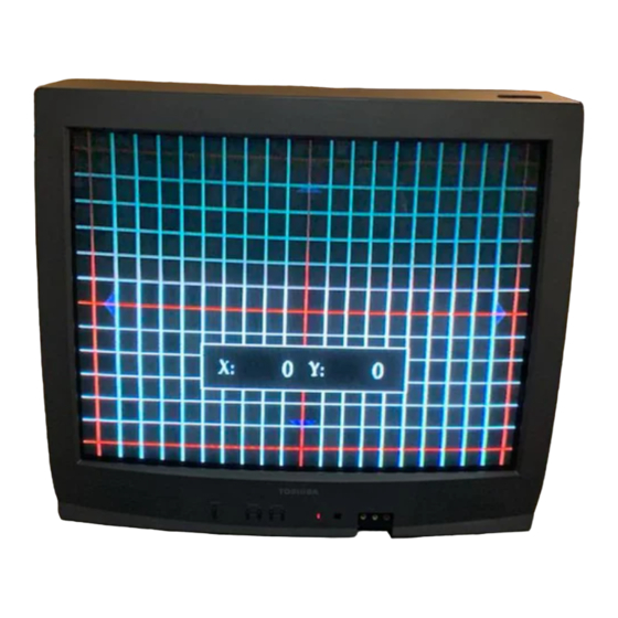
ELECTRICAL ADJUSTMENTS PURITY AND CONVERGENCE 3-3: STATIC CONVERGENCE ADJUSTMENTS NOTE Adjust after performing adjustments in section 3-2. NOTE Receive the crosshatch pattern from the color bar Turn the unit on and let it warm up for at least 30 generator. minutes before performing the following adjustments. -
Page 14: Major Components Location Guide
MAJOR COMPONENTS LOCATION GUIDE VR502 T501 TP002 VR401 FB401 J702 FOCUS VOLUME SCREEN VOLUME MAIN PCB TP804 J801 TP806 CRT PCB... -
Page 15: Tv Block Diagram
TV BLOCK DIAGRAM SPEAKER SP1001 TU001 MICON IC101 OEC7054A SOUND AMP IC1001 AN5276 YUV IN IF/CHROMA/AUDIO IC201 TB1253N 24 25 43 44 18 19 V OUT IC902 AN5829S TONE CONTROL IC303 10 SCL M62420SP COMB FILTER IC1501 TC90A45F YUV IN S INPUT AV SWITCH IC701... -
Page 16: Q1504
PRINTED CIRCUIT BOARDS COMB SOLDER SIDE (INSERTED PARTS) (CHIP MOUNTED PARTS) SOLDER SIDE SOLDER SIDE TP805 R806 Q811 C815 D802 R1510 Q1504 R814 R809 R1517 R812 R1516 W002 D809 D808 R1509 C1521 Q1502 Q1503 IC1501 D807 R1505 R1513 R802 CP804 C1513 R1501 C1522... -
Page 17: W807
PRINTED CIRCUIT BOARDS MAIN/VIDEO JACK (INSERTED PARTS) SOLDER SIDE CD801 CP801A W122 J702 C418 CP101 S101X J701 J703 J704 J203 TP001 D411 W172 R441 TP901 R437 C425_1 C002 W068 CP401_1 FB401 IC701 S103X C735 C713 W072 S101Y W152 W153 Q405 W140 C413_1 TP002... - Page 18 PRINTED CIRCUIT BOARDS MAIN/VIDEO JACK (CHIP MOUNTED PARTS) SOLDER SIDE R104 R727 Q509 Q704 Q705 R510 C331 C332 R121 R324 C334 R532 C330 C333 C926 R327 R127 R905 R116 Q101 R904 IC902 Q102 R140 C112 C138 C927 R118 R144 R906 R150 R747 C132...
-
Page 19: Buffer
MICON / TUNER SCHEMATIC DIAGRAM (MAIN PCB) OS101 TU001 ENV56D66G3 ACCESORY PIC-28143SY-2 BT001 R03(AB)E_20_T R003 TM101 330K BT002 SBKMOP006A R03(AB)E_20_T C003 H-BUFFER Q102 TP001 FROM/TO CHROMA/IF 2SC2412K RED LED V-BUFFER POWER ON Q101 2SC2412K MICON D109 R139 IC101 OEC7054A SLR-342VCT32 OSD_R R123 1K 1/4W... -
Page 20: W802
CHROMA / IF SCHEMATIC DIAGRAM (MAIN PCB) FROM/TO AV C.OUT Y.OUT FROM/TO MICON/TUNER TUNER_VIDEO R214 C613 SYNC_OUT FSC_OUT TUNER_AUDIO_L AUDIO TUNER_AUDIO_R BUFFER C213 Q201 V.KILLER W813 2SC2412K Q601 OSD_B W808 DTC114EKA FROM/TO AV OSD_G C615 R608 W802 CD701B OSD_R CH243001 D601 C212 H_TONE_H... - Page 21 DEFLECTION SCHEMATIC DIAGRAM (MAIN PCB) V.OUTPUT IC401 LA78041 THERMAL PROTECTION PUMP UP 25.0 12.0 25.0 R407 3.9K 1/4W C411 R414 500V 27K +-1% R417 33K R408 V801 A68AJB82X10 1/2W SWITCH Q107 KRC111RTK HS402 FROM/TO DY FROM/TO POWER 763WAA0216 CP401_1 P.CON+5V W827 TS-80P-04-V1 R152...
-
Page 22: Power Schematic Diagram
POWER SCHEMATIC DIAGRAM 6.3A 125V CAUTION: FOR CONTINUED PROTECTION AGAINST FIRE HAZARD, REPLACE ONLY WITH THE SAME TYPE FUSE 6.3A 125V(F501) ATTENTION: POUR UNE PROTECTION CONTINUE LES RISQUES D’INCEIE N’UTILISER QUE DES FUSIBLE DE MEME TYPE 6.3A 125V(F501) (MAIN PCB) D516 RELAY DRIVE Q504... - Page 23 SOUND SCHEMATIC DIAGRAM (MAIN PCB) FROM/TO AV R314 AUDIO_R R324 C334 AUDIO_L 1.8K 0.033 B C332 R326 C331 0.47 B 0.022 R328 1.8K TONE 136K AMP1 I2C BUS INTERFACE SIMAMP1 VOLAMP1 6.5K 6.5K 6.5K VOLAMP2 CONTROL SIMAMP2 6.5K LOGIC TONE 136K 1.8K AMP2...
-
Page 24: Cp1501
AV SCHEMATIC DIAGRAM FROM/TO CHROMA/IF (MAIN PCB) CD701A CH243001 YUV_IN(REAR) J704 AV3-19D-5 FROM/TO COMB FILTER CP1501 6035B-06Z002-T MONITOR V.OUT A/V_OUT(REAR) Y IN J203 C IN AV3-19DS-1 P.CON+5V LINE2(REAR) J703 FROM/TO POWER AV3-19DS-1 L703 P.CON+9V 47uH P.CON+5V 0305 C713 R751 GND_POWER C714 R752 C715... - Page 25 CRT SCHEMATIC DIAGRAM (CRT PCB) FROM DEFLECTION TP804 R828 CP805_1 (CP801A) A2001WV2-10P 2.7K 1/4W RED AMP Q801 123.5 P.CON+9V R813 2SC2621 G.OUT 220 1/4W R.OUT 121.0 B.OUT 582.0 D801 HEATER 117.0 1SS133 RED AMP Q810 119.0 R801 2SC1740SP 100 1/4W R810 180V C813...
-
Page 26: Table Of Contents
DIGITAL COMB FILTER SCHEMATIC DIAGRAM (COMB PCB) BUFFER C1525 L1506 R1511 Q1504 2SC2412K 22uH C1511 L1503 W803 820uH C1506 FROM/TO 0.01 B CP1501 6035B-06Z002-T MONITOR V.OUT Y IN C IN W807 P.CON+5V BUFFER Q1502 2SA1037AK C1501 W802 BUFFER Q1503 0.1 B BUFFER 2SC2412K Q1501... - Page 27 WAVEFORMS MICON/TUNER 2.0V 50ns/div 500mV 10µs/div 500mV 50µs/div 2.0V 50ns/div 200mV 10µs/div 100mV 100ns/div 1.0V 5ms/div 2.0V 50µs/div 1.0V 20µs/div 2.0V 50µs/div 1.0V 20µs/div 1.0V 20µs/div CHROMA/IF 200mV 10µs/div 2.0V 20µs/div 1.0V 20µs/div NOTE: The following waveforms were measured at the point of the corresponding balloon number in the schematic diagram.
- Page 28 WAVEFORMS DEFLECTION 1.0V 5ms/div 200V 20µs/div 500mV 1ms/div SOUND 10V 5ms/div 1.0V 2ms/div 500mV 1ms/div 10V 5ms/div 1.0V 2ms/div 200mV 20µs/div 50V 20µs/div 20mV 1ms/div 200mV 20µs/div 2.0V 20µs/div 20mV 1ms/div 100mV 10µs/div NOTE: The following waveforms were measured at the point of the corresponding balloon number in the schematic diagram.
- Page 29 50V 10µs/div 500mV 10µs/div 1.0V 1ms/div 50V 10µs/div 1.0V 1ms/div 1.0V 10µs/div 50V 10µs/div NOTE: The following waveforms were measured at the point of the corresponding balloon number in the schematic diagram.
-
Page 30: Mechanical Exploded View
MECHANICAL EXPLODED VIEW J801 PCB110 (CRT PCB) L503 FB401 V801 TU001 PCB010 PCB330 (MAIN PCB) (COMB PCB) SP1001 PCB170 (VIDEO JACK PCB) -
Page 31: Mechanical Replacement Parts List
MECHANICAL REPLACEMENT PARTS LIST Location No. TSB P/N Reference No. Description AD300756 A3K106E720 CABINET,FRONT ASSY AD300757 771WPA0263 PLATE,JACK AD300758 899EFBA001 WIRING CLIP BZ710260 899HV3T000 HOLDER,ANODE WIRE AD300759 741WUA0021 SPRING,EARTH AD300760 701APJ0082 CABINET,FRONT AD300761 712APB0001 DOOR AD300762 702APA0128 CABINET,BACK AD300763 711WPA0149 PLATE,FRONT AD300764 713WPA0163... -
Page 32: Electrical Replacement Parts List
ELECTRICAL REPLACEMENT PARTS LIST Location No. TSB P/N Reference No. Description RESISTORS ! R416 AD300416 R002T25R6J 5.6 OHM 1/2W ! R418 BZ210105 R4X5T6183F R,METAL 18K OHM 1/6W ! R420 BZ210053 R002T22R2J 2.2 OHM 1/2W ! R422 BZ210013 R4X5T4104F R,METAL 100K OHM 1/4W ! R426 BZ210105 R4X5T6183F... - Page 33 ELECTRICAL REPLACEMENT PARTS LIST Location No. TSB P/N Reference No. Description DIODES ! D411 BZ410063 D2WTAU02A0 DIODE,SILICON AU02A-EIC ! D501 BZ410085 D2WXN40050 DIODE,SILICON 1N4005-EIC ! D502 BZ410085 D2WXN40050 DIODE,SILICON 1N4005-EIC ! D503 BZ410085 D2WXN40050 DIODE,SILICON 1N4005-EIC ! D504 BZ410085 D2WXN40050 DIODE,SILICON 1N4005-EIC ! D505...
- Page 34 ELECTRICAL REPLACEMENT PARTS LIST Location No. TSB P/N Reference No. Description TRANSISTORS Q509 BZ510071 TNAAB05003 COMPOUND TRANSISTOR KRC102RTK ! Q510 BZ510031 TD3T007340 TRANSISTOR,SILICON 2SD734(E,F)-AA ! Q512 BZ510004 TA3T016240 TRANSISTOR,SILICON 2SA1624-AA Q601 BZ510020 TNYJB05001 COMPOUND TRANSISTOR DTC114EKAT146 Q603 BZ510002 T8YJ2412K0 TRANSISTOR,SILICON 2SC2412KT146 R,S Q604 BZ510002...
- Page 35 ELECTRICAL REPLACEMENT PARTS LIST Location No. TSB P/N Reference No. Description MISCELLANEOUS ! CD501 AD300746 120R615901 CORD AC BUSH 0R615901 CD702 AD300747 06CU252002 CORD CONNECTOR CU252002 CD801 AD300748 06CU2A3401 CORD CONNECTOR CU2A3401 CD803 BZ614175 06CU82039A CORD CONNECTOR SM1098-009-1A CD805 BZ614175 06CU82039A CORD CONNECTOR SM1098-009-1A...
- Page 36 TOSHIBA AMERICA CONSUMER PRODUCTS,INC. HEAD OFFICE / 82 TOTOWA ROAD,WAYNE,NEW JERSEY 07470 U.S.A.
Need help?
Do you have a question about the 27A41 and is the answer not in the manual?
Questions and answers