Advertisement
CTK-620L
100 RHYTHMS
RHYTHMS
TONE
137 TONES
MODE
VOLUME
INTRO
SYNCHRO/ENDING
TEMPO
MAX
POWER
FULL RANGE
CHORD
FINGERED
CASIO CHORD
NOMAL
MIN
NORMAL/FILL-IN
VARIATION/FILL-IN
START/STOP
ELECTRONIC KEYBOARD
100 SONG BANK
MUSICAL INFORMATION SYSTEM
REVERB
HALL
GM
STAGE
LAYER
ROOM
SPLIT
TOUCH
MEMORY
RESPONSE
SPLIT
RHYTHM
KEY LIGHT
STEP
SONG BANK CONTROLLER
KEY LIGHT
STOP
PLAY/PAUSE
REW
FF
SONG
BANK
SONG BANK
3
(TIE)
7
8
9
TONE
4
5
6
TRACK 1
TRACK 2
DEMO
LEFT
RIGHT
1
2
3
3-STEP LESSON
STEP 1
STEP 2
STEP 3
REST
1
2
3
0
CTK-620L
Advertisement
Table of Contents

Related Manuals for Casio CTK-620L


Summary of Contents for Casio CTK-620L
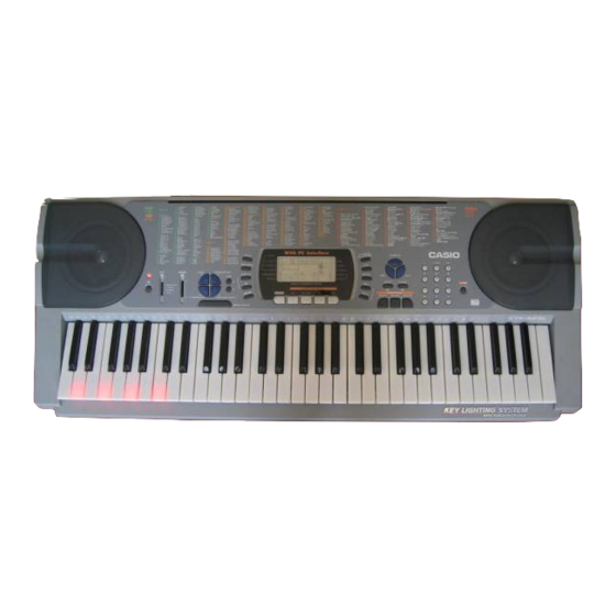
- Page 1 CTK-620L 100 RHYTHMS 100 SONG BANK RHYTHMS SONG BANK TONE 137 TONES MUSICAL INFORMATION SYSTEM SONG BANK REVERB HALL (TIE) STAGE LAYER ROOM SPLIT MODE VOLUME INTRO SYNCHRO/ENDING TOUCH MEMORY RESPONSE SPLIT RHYTHM TONE TEMPO KEY LIGHT STEP TRACK 1...
-
Page 2: Table Of Contents
3 reverb types (HALL, STAGE, ROOM) Auto accompaniment Rhythm patterns: Tempo: Variable (216 steps, = 40 to 255) Chords: 3 fingering methods (CASIO CHORD, FINGERED, FULL RANGE CHORD) Rhythm controller: START/STOP, INTRO, NORMAL/NORMARL FILL-IN, VARIATION/ VARIATION FILL-IN, SYNCHRO/ENDING Accomp volume:... - Page 3 Power jack 9 V DC Power supply: 2-way Batteries: Six D-size batteries Battery life: Approximately 5 hours continuous operation on manganese batteries AC adaptor: AD-5 Auto power off: Turns power off approximately six minutes after last key operation. En- abled under battery power only, can be disabled manually. Speaker output: 2.5 W + 2.5 W Power consumption:...
-
Page 4: Block Diagram
BLOCK DIAGRAM SEG1 ~ SEG40 Working Storage LCD Driver RAM (256K-bit) MIDI PO10, PO17 LSI4 LSI401 PO22, PO23 TC55257DFL-70L(EL) SED1278F0A PA4 ~ PA6 COM1 ~ COM16 RACEB Reset IC IC1 RESET RN5VD40AA FI0 ~ FI7 Illuminant SI0 ~ SI7 MA14 KC0 ~ KC7 Keyboard Sound Source ROM... -
Page 5: Circuit Description
METRO STEP 1 DEMO TOUCH REVERB TRACK 1/ PLAY/PAUSE STOP LAYER RHYTHM KEYLIGHT RIGHT TRANSPOSE/ TRACK 1/ REWIND FI10 SPLIT SONG LEFT TUNE/MIDI FULL RANGE INTRO CHORD NORMAL FINGERED FILL-IN CASIO VARIATION CHORD FILL-IN START/ NORMAL STOP — 4 —... - Page 6 LED MATRIX Note: Each key has two contacts, the first conatct (1) and second contact (2). First contact (1) Second contact (2) NOMENCLATURE OF KEYS F#3 G#3 A#3 C#4 D#4 F#4 G#4 A#4 C#5 D#5 F#5 G#5 A#5 C2 D2 G2 A2 C3 D3 G3 A3...
-
Page 7: Power Supply Circuit
POWER SUPPLY CIRCUIT The power supply circuit generates seven voltages as shown in the following table. VDD voltage is always generated. The others are controlled by APO signal from the CPU. t l i i f i l RESET CIRCUIT When batteries are set or an AC adapter is connected, the reset IC provides a low pulse to the CPU. - Page 8 CPU (LSI1: GT913F) The 16-bit CPU contains a 1k-byte RAM, three 8-bit I/O ports, two timers, a key controller and serial interfaces. The CPU detects key velocity by counting the time between first-key input signal FI and second-key SI from the keyboard.
- Page 9 DIGITAL SIGNAL PROCESSOR (LSI2: HG51B227FB-1) The DSP receives 16-bit serial sound data output from the CPU and adds the selected effect to the sound data using the effect RAM. Then the DSP provides the sound data to the DAC. The DSP also controls button input/ output and GA.
- Page 10 Pin No. Terminal In/Out Function CE1B Chip enable signal input. Low active. 35 ~ 41, 43 EIO0 ~ EIO7 In/Out Data bus for the effect RAM 42 , 44, 46 ~ 48, EA0 ~ EA14 Address bus for the effect RAM 51 ~ 59, 61 ECEB Chip enable signal output for the effect RAM...
- Page 11 GATE ARRAY (LSI7: UPD65005GF-419) The gate array can control 63 LEDs of key illuminators. In accordance with the command from the CPU, the LSI is capable of controlling the illuminator LEDs. The following table shows the pin functions of LSI7. —...
- Page 12 FILTER BLOCK Since the sound signals from the DAC are stepped waveforms, the filter block is added to smooth the waveforms. AVDD AVDD 2SC1740SQ.R 50 V 0.22 µ 3.3K 4.7K From DAC 12 µF 50 V 3.3 µ To main volume POWER AMPLIFIER (IC101: TA8248K) The power amplifier is a two-channel amplifier with standby switch.
-
Page 13: Adjustment
ADJUSTMENT DISPLAY PCB 1) Items to be adjusted: 2) Adjustment and Test Point Locations VR401 (TOP VIEW) 3) Equipment connection/Procedure Vop voltage setting Voltmeter Output Input Input Output Output Input Adjust Adjust for Connection Point Signal Connection Point VR401 Voltmeter Adjust for 4.2 ~ 4.3 V reading on voltmeter under the tem- perature 20 ~ 25 °C. -
Page 14: Major Waveforms
MAJOR WAVEFORMS 1 Clock signal B1 3 MNI signal 5 LED common signal L23 Test point T5 JM connector pin 18 JN connector pin 1 2 Clock signal B2 4 APOFF signal 6 LED common signal L22 Test point T6 JS connector pin 12 JN connector pin 2 Key : C7... -
Page 15: Printed Circuit Boards
PRINTED CIRCUIT BOARDS Sub PCB JCM447-MA2M Main PCB JCM447-MA1M Top View Bottom View — 14 —... -
Page 16: Schematic Diagrams
SCHEMATIC DIAGRAMS Main PCB JCM447-MA1M — 15 —... - Page 17 Sub PCB JCM447-MA2M (5.6 V) (0.7 V) (5.6 V) (5.6 V) (2 V) — 16 —...
- Page 18 Console PCB JCM447-CN1M — 17 —...
- Page 19 Console PCB JCM447-CN2M — 18 —...
- Page 20 Display PCB JCM447-LCD1M — 19 —...
- Page 21 Keyboard PCBs JCM618T-KY1M/KY2M — 20 —...
- Page 22 LED PCB JCM447-LD1M — 21 —...
- Page 23 LED PCB JCM447-LD2M — 22 —...
- Page 24 LED PCB JCM447-LD6 — 23 —...
- Page 25 Console PCBs JCM447-CN3M/CN4M — 24 —...
- Page 26 Console PCB JCM447-CN5M — 25 —...
- Page 27 LED PCBs JCM447-LD4M/LD5M — 26 —...
- Page 28 LED PCB JCM447-LD3M — 27 —...
-
Page 29: Exploded View
EXPLODED VIEW 32 24 — 28 —... -
Page 30: Parts List
PARTS LIST CTK-620L Notes: This parts list does not include the cosmetic parts, which parts are marked with item No. "R-X" in the exploded view. Contact our spare parts department if you need these parts for refurbish. Prices and specifications are subject to change with- out prior notice. - Page 31 Item Code No. Parts Name Specification Main PCB 2012 1883 IC/MOS RN5VD40AA-TR 2105 6427 IC/L-MOS TC7WH04FUTE12L 2105 4935 IC/C-MOS TC74VHV08F(TP1) LSI1 2012 5005 LSI/MC GT913F(T) LSI2 2012 4494 LSI HG51B277FB-1 LSI3 2012 5915 LSI LH536PNV LSI4/LSI5 2012 5572 LSI/S-RAM T055257DFL-70L(EL) LSI6 2105 4746 LSI/D-A CONVERTER UPD6379GR-E1...
- Page 32 Item Code No. Part Name Specification 6926 3150 M446-LD5M PCB ASSY M240430*2 6926 3160 M447-LD1M PCB ASSY M240777*1 6926 3170 M447-LD2M PCB ASSY M240778*1 Keyboard unit 6925 1700 KEY SET/WHITE/LSK-CB M340489*1 6925 1710 KEY SET/WHITE/LSK-CS M340489*2 6925 1720 KEY SET/BLACK LSK10P M140369-1 6925 1730 KEY SET/BLACK LSK5P M140369-2...
- Page 33 CASIO TECHNO CO.,LTD. 8-11-10, Nishi-Shinjuku Shinjuku-ku, Tokyo 160, Japan Nov. 1997 Telephone: 03-3347-4926 MA1100571A Printed in Japan...
Need help?
Do you have a question about the CTK-620L and is the answer not in the manual?
Questions and answers