Aiwa NSX–BL24 Service Manual
Compact disc stereo system
Hide thumbs
Also See for NSX–BL24:
- Service manual (37 pages) ,
- Service manual (43 pages) ,
- Service manual (43 pages)
Table of Contents
Advertisement
SERVICE MANUAL
COMPACT DISC STEREO SYSTEM
SYSTEM
NSX–BL24
• If requiring information about the CD mechanism, see Service Manual of AZG-1,
(S/M Code No. 09-001-335-3N8).
NSX-BL24
BASIC TAPE MECHANISM : ZZM-3 YPR1NC
BASIC CD MECHANISM : AZG-1 ZD4RDC
CD
CASSEIVER
CX–NBL24
S/M Code No. 09-00A-426-1N1
REMOTE
SPEAKER
CONTROLLER
SX–NBL25
RC–ZAS02
G
Advertisement
Table of Contents

Related Manuals for Aiwa NSX–BL24


Summary of Contents for Aiwa NSX–BL24
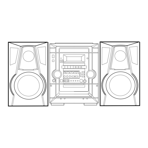
- Page 1 NSX-BL24 SERVICE MANUAL BASIC TAPE MECHANISM : ZZM-3 YPR1NC COMPACT DISC STEREO SYSTEM BASIC CD MECHANISM : AZG-1 ZD4RDC REMOTE SYSTEM SPEAKER CASSEIVER CONTROLLER NSX–BL24 CX–NBL24 SX–NBL25 RC–ZAS02 • If requiring information about the CD mechanism, see Service Manual of AZG-1, (S/M Code No.
-
Page 2: Specifications
SPECIFICATIONS Main unit CX-NBL24 <Compact disc player section> Laser Semiconductor laser (λ =780 nm) <FM Tuner section> D/A converter 1 bit dual Tuning range 87.5 MHz to 108 MHz Signal-to-noise ratio 85 dB (1 kHz, 0 dB) Usable sensitivity (IHF) 16.8 dBf Harmonic distortion 0.05 % (1 kHz, 0 dB) -
Page 3: Protection Of Eyes From Laser Beam During Servicing
PROTECTION OF EYES FROM LASER BEAM DURING SERVICING CAUTION This set employs laser. Therefore, be sure to follow carefully the instructions below when servicing. Use of controls or adjustments or performance of proce- dures other than those specified herin may result in WARNING!! hazardous radiation exposure. -
Page 4: Note On Before Starting Repair
NOTE ON BEFORE STARTING REPAIR 1. Forced discharge of electrolytic capacitor of power supply block When repair is going to be attempted in the set that uses relay circuit in the power supply block, electric potential is kept charged across the electrolytic capacitors (C101, 102) even though AC power cord is removed. - Page 5 In such a case, check also if the POWER AMPLIFIER circuit or power supply circuit has any abnormalities or not. 2-2. Regarding reset There are cases that the machine does not work correctly because the MICROCOMPUTER is not reset even though the AC power cord is re-inserted, or the software reset (pressing the STOP key + POWER key) is performed.
-
Page 6: Electrical Main Parts List
ELECTRICAL MAIN PARTS LIST REF. NO. PART NO. KANRI DESCRIPTION REF. NO. PART NO. KANRI DESCRIPTION 87-010-196-080 CHIP CAPACITOR,0.1-25 87-010-196-080 CHIP CAPACITOR,0.1-25 87-A21-269-010 IC,EW732 C101 87-010-185-080 C-CAP,S 3900P-50 B 87-A21-396-010 IC,STK490-040 C102 87-010-185-080 C-CAP,S 3900P-50 B 87-A21-419-040 C-IC,NJM14558MD-TE2 C103 87-010-545-080 CAP,ELECT 0.22-50V 87-A21-401-040 C-IC,M61503FP... - Page 7 REF. NO. PART NO. KANRI DESCRIPTION REF. NO. PART NO. KANRI DESCRIPTION C461 87-012-158-080 C-CAP,S 390P-50 CH C860 87-010-197-080 CAP,CHIP 0.01 DM C462 87-012-158-080 C-CAP,S 390P-50 CH C940 87-010-197-080 CAP,CHIP 0.01 DM C470 87-018-127-080 CAP,TC U 470P-50 KB C942 87-010-149-080 C-CAP,S 5P-50 CH C605 87-010-179-080...
- Page 8 REF. NO. PART NO. KANRI DESCRIPTION REF. NO. PART NO. KANRI DESCRIPTION 8A-NF9-609-010 F-CABLE,9P 2.5 480MM S304 87-A90-164-080 SW,TACT SKQNAB(N) 87-A90-510-010 HLDR,WIRE 2.5-9P S305 87-A90-164-080 SW,TACT SKQNAB(N) X991 87-A70-061-010 VIB,XTAL 4.500MHZ CSA-309 S306 87-A90-164-080 SW,TACT SKQNAB(N) S307 87-A90-164-080 SW,TACT SKQNAB(N) S308 87-A90-164-080 SW,TACT SKQNAB(N)
-
Page 9: Chip Resistor Part Code
CHIP RESISTOR PART CODE Chip Resistor Part Coding Figure Resistor Code Value of resistor Chip resistor Dimensions (mm) Symbol Wattage Type Tolerance Resistor Code Form 1/16W 1005 0.35 1/16W 1608 0.45 1/10W 2125 1.25 0.45 1/8W 3216 0.55 TRANSISTOR ILLUSTRATION E C B E C B E C B... -
Page 10: Pin Connection
FL (HNA–10SS12) GRID ASSIGNMENT / ANODE CONNECTION / PIN CONNECTION GRID ASSIGNMENT ANODE CONNECTION PIN CONNECTION – 10 –... -
Page 11: Wiring - 1 (Main)
WIRING – 1 (MAIN) – 11 –... -
Page 12: Schematic Diagram - 1 (Main : 1 / 2 )
SCHEMATIC DIAGRAM – 1 (MAIN : 1 / 2 <AMP SECTION>) – 12 –... -
Page 13: Schematic Diagram - 2 (Main : 2 / 2 )
SCHEMATIC DIAGRAM – 2 (MAIN : 2 / 2 <TUNER SECTION>) – 13 –... -
Page 14: Wiring - 2 (Front)
WIRING – 2 (FRONT) – 14 –... -
Page 15: Schematic Diagram - 3 (Front / Deck)
SCHEMATIC DIAGRAM – 3 (FRONT / DECK) – 15 –... - Page 16 WIRING – 3 (PT) – 16 –...
-
Page 17: Schematic Diagram - 4 (Pt)
SCHEMATIC DIAGRAM – 4 (PT) – 17 –... - Page 18 WIRING – 4 (DECK) FROM B FRONT C. B CN104 FFC104 D DECK C . B 1 3 5 7 9 11 2 4 6 8 10 – 18 –...
-
Page 19: Ic Block Diagram
IC BLOCK DIAGRAM – 19 –... - Page 20 IC DESCRIPTION µ PD780226GF-019-3BA Pin No. Pin Name Description O-MOTOR DECK MOTOR ON/OFF output. O-SOL1 DECK1 solenoid output. O-SOL2 DECK2 solenoid output. – Not connected. – Not connected. O-SET_LED SET LED ON/OFF output. O-CLEAR_LED CLEAR LED ON/OFF output. O-PRESET_LED PRESET LED ON/OFF output. O-DOWN_LED DOWN LED ON/OFF output.
- Page 21 Pin No. Pin Name Description I-HOLD Power failure detected input. I-CDSW CD mecha switch input. I-SPEANA_L A/D L-input for spectrum analyser level display. I-SPEANA_R A/D R-input for spectrum analyser level display. I-KEY1 Key1 input. I-KEY2 Key2 input. I-KEY3 Key3 input. I-TU_SIG Tuner signal input.
- Page 22 IC, LC72131D Pin No. Pin Name Description X-IN A crystal oscillator (4.5MHz) is connected between these pins. X-OUT – Not connected. To enable the IC. Active "H". Digital data input from CPU (µPD780226GF-019-3BA) when relevant key is operated. Active "H". To clock in the data DI.
- Page 23 ADJUSTMENT – 1 <TUNER / FRONT> < TUNER SECTION > 1. Clock frequency Check 9. DC Balance / Mono Distortion Adjustment Settings : • Test point : TP2 (CLK) Settings : • Test point : TP3, TP4 (DC) Method : Set to MW 1602kHz and check that the test point is •...
- Page 24 ADJUSTMENT – 2 <DECK> < DECK SECTION > 1. Tape Speed Adjustment (DECK 2) 5. REC/PB Frequency Response Adjustment (DECK 2) Settings : • Test tape : TTA–100 Settings : • Test tape : TTA–602 • Test point : TP8 (Lch), TP9 (Rch) •...
-
Page 25: Mechanical Exploded View
MECHANICAL EXPLODED VIEW 1 / 1 AZG-1 ZD4RDC WIRE,BINDER FL901 HT-SINK PLATE SHLD PT 2T PLATE,EARTH MIC CHAS,MAIN ZZM-3 YPR1NC PLATE,EARTH MECHA C – 25 –... -
Page 26: Mechanical Parts List
MECHANICAL PARTS LIST 1 / 1 REF. NO. PART NO. KANRI DESCRIPTION REF. NO. PART NO. KANRI DESCRIPTION 1 8A-NF0-007-010 WINDOW,CASS 2 26 8A-NF0-008-010 KEY,POWER 2 8A-NF0-006-010 WINDOW,CASS 1 27 8A-NF0-201-010 GUIDE,OPE 1 WAY 3 8A-NF0-004-010 BOX,CASS 2 28 82-NF7-210-110 GUIDE,FL (*) 4 8A-NF0-003-010 BOX,CASS 1... -
Page 27: Tape Mechanism Exploded View
TAPE MECHANISM EXPLODED VIEW 1 / 1 TERMINAL,LB1 TERMINAL, IC, EW732 IC, EW732 – 27 –... -
Page 28: Tape Mechanism Parts List
TAPE MECHANISM PARTS LIST 1 / 1 REF. NO. PART NO. KANRI DESCRIPTION REF. NO. PART NO. KANRI DESCRIPTION 8Z-ZM3-227-010 BELT,MAIN M3 8Z-ZM3-233-010 SPR-T,BRG M3 8Z-ZM3-235-010 BELT,MAIN L 84-ZM2-227-310 SPR-C,AZIMUTH 8Z-ZM1-235-010 PULLEY,MOT 87-A90-403-110 HEAD,RPH MS15R 87-045-347-010 MOT,SHU2L 70 87-A90-404-010 HEAD,EH LE15B 8Z-ZM1-232-010 GEAR,IDL FF/REW 8Z-ZM3-239-010... -
Page 29: General Speaker Disassembly Instructions (For Reference)
GENERAL SPEAKER DISASSEMBLY INSTRUCTIONS (FOR REFERENCE) Type.1 Type.4 TOOLS Insert a flat-bladed screwdriver into the position indicated by the arrows and remove the panel. Remove the screws of each speaker 1 Plastic head hammer unit and then remove the speaker units. 2 (() flat head screwdriver 3 Cut chisel How to Remove the PANEL, FR... -
Page 30: Speaker Parts List
GRILLE,FRAME ASSY 4 8A-NSK-602-010 SPKR,W 140 5 8A-NSK-606-010 SPKR,T 60 6 87-NSH-612-010 SPKR,CERAMIC ASSY 7 87-NS7-611-010 CORD,SPKR 8 8A-NSJ-006-010 BADGE,AIWA S35 ACCESSORIES / PACKAGE LIST REF. NO. PART NO. KANRI DESCRIPTION 1 8A-NF0-904-010 IB,G(E)FM-BL24 2 87-A90-118-010 ANT,WIRE FM(Z) 3 87-A90-030-010... - Page 31 2–11, IKENOHATA 1–CHOME, TAITO-KU, TOKYO 110, JAPAN TEL:03 (3827) 3111 9420025 0251431 Printed in Singapore...
Need help?
Do you have a question about the NSX–BL24 and is the answer not in the manual?
Questions and answers