Table of Contents
Advertisement
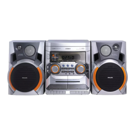
Mini System
Service
Service
Service
Service
Service
Service Manual
©
Copyright 2002 Philips Consumer Electronics B.V. Eindhoven, The Netherlands
All rights reserved. No part of this publication may be reproduced, stored in a retrieval system or
transmitted, in any form or by any means, electronic, mechanical, photocopying, or otherwise
without the prior permission of Philips.
Published by KC 0201 Service Audio
Version 1.0
TABLE OF CONTENTS
Location of pc boards & Version variations ................ 1-2
Technical Specifications ............................................. 1-3
Measurement setup .................................................... 1-4
Disassembly Instructions & Service positions .............. 2
Service Test Programs & DEMO mode ......................... 3
Set Block diagram ......................................................... 4
Set Wiring diagram ........................................................ 5
Front Board .................................................................... 6
Mains Board ................................................................... 8
ECO-MTF Module .......................................................... 9
3CDC-LC-MB Module .................................................. 10
Combi Board ................................................................ 11
Set Mechanical Exploded view & parts list ................. 12
Printed in The Netherlands
Subject to modification
FW-C255/
Page
CLASS 1
LASER PRODUCT
GB
21/30/37
COMPACT
DIGITAL AUDIO
3139 785 30021
Advertisement
Chapters
Table of Contents

Related Manuals for Philips FW-C255


Summary of Contents for Philips FW-C255
-
Page 1: Table Of Contents
LASER PRODUCT © Copyright 2002 Philips Consumer Electronics B.V. Eindhoven, The Netherlands All rights reserved. No part of this publication may be reproduced, stored in a retrieval system or transmitted, in any form or by any means, electronic, mechanical, photocopying, or otherwise without the prior permission of Philips. - Page 2 LOCATION OF PC BOARDS VERSION VARIATIONS: Type /Versions: FW-C255 /21M Features & Board in used: Karaoke News Incredible Surround Rotary Encoder (volume control) Jog Shuttle Voltage Selector Aux Input Digital Output Headphone Socket Line Output Subwoofer Output Surround Output Matrix Surround Loudspeakers...
- Page 3 SPECIFICATIONS GENERAL: Mains voltage : 110-127V/220-240V Switchable for /21/21M CASSETTE RECORDER: 120V for /37 Number of track : 2 x 2 stereo 230-240V for /30 Tape speed : 4.76 cm/sec +2.5/-1.5% Mains frequency : 50/60Hz Wow and flutter : < 0.35% DIN Power consumption : <...
-
Page 4: Measurement Setup
MEASUREMENT SETUP Tuner FM Bandpass LF Voltmeter 250Hz-15kHz e.g. PM2534 e.g. 7122 707 48001 RF Generator e.g. PM5326 S/N and distortion meter e.g. Sound Technology ST1700B Use a bandpass filter to eliminate hum (50Hz, 100Hz) and disturbance from the pilottone (19kHz, 38kHz). Tuner AM (MW,LW) Bandpass LF Voltmeter... -
Page 5: Service Aids
SERVICE AIDS Service Tools: ESD Equipment: Universal Torx driver holder ........4822 395 91019 Anti-static table mat - large 1200x650x1.25mm ... 4822 466 10953 Torx bit T10 150mm ..........4822 395 50456 Anti-static table mat - small 600x650x1.25mm ..4822 466 10958 Torx driver set T6 - T20 ......... - Page 6 WAARSCHUWING WARNING Alle IC’s en vele andere halfgeleiders zijn All ICs and many other semi-conductors are gevoelig voor electrostatische ontladingen susceptible to electrostatic discharges (ESD). (ESD). Careless handling during repair can reduce life Onzorgvuldig behandelen tijdens reparatie kan drastically. de levensduur drastisch doen verminderen. When repairing, make sure that you are Zorg ervoor dat u tijdens reparatie via een connected with the same potential as the mass...
- Page 7 DISMANTLING INSTRUCTIONS Dismantling of the Front Panel assembly Dismantling the 3CDC Module 1) Loosen the 4 screws, slide Cover top (pos 253) towards 4) Remove the Cover Tray (pos 105) as shown in figure 2. 1) Loosen 2 screws below the Front Panel (pos 101) mounting 4) Loosen 8 screws B to remove the Front board as shown in the rear and remove it upwards.
- Page 8 Dismantling of the Cassette door Lenses Service pos A 1) Loosen the Lens Cassette Strip Left Top (pos 163) by 2) Remove the Lens Cassette Left (pos 161) by pushing it towards the inside as indicated in Figure 7. Be careful not pushing it towards the inside as indicated in Figure 7 and to damage or break the catch A.
- Page 9 SERVICE TEST PROGRAM To start service test program hold P & TAPE depressed while plugging in the mains cord S refers to Service Mode. Display shows the ROM version * V refers to Version. "S-Vyy" (Main menu) yy refers to Software version number of Processor. (Counting up from 01 to 99) Mini 2002 FW-C1xx, C2xx, C3xx Dated: wk141 TUNER...
-
Page 10: Set Block Diagram
# VCD CONTROL REGULATOR SA IN L7805 KEY SCAN (+5V) MATRIX -33V CD_ON # FOR VCD/MP3 VERSION MIC DET +5V6_ECO SMPS +5V6 HP DET 650mV 78dBA 3.2dB HP DET MUTE HP_MUTE FW-C255 Block diagram ...34280 dd wk148 HEADPHONE FRONT HP_OUT... -
Page 11: Set Wiring Diagram
MATRIX # - PROVISION FOR SETS WITH VCD/MP3 FEATURE . SURROUND FW-C255 Wiring diagram ... 34280 dd wk148 (NOT USA) (USA) ## - PROVISION FOR SETS WITH MATRIX SURROUND. $$ - PROVISION FOR SETS WITH ECO FEATURE (ONLY FOR -/22 VER.) . -
Page 12: Front Board
FTD DISPLAY PIN CONNECTIONS FRONT BOARD Col 1 (12G) (11G) (2G - 9G) TABLE OF CONTENTS Variation Table and FTD Display pin connection .... 6-1 Chip Layout ..............6-2 (Left) Component Layout ............6-3 j , p j , p j , p j , p j , p... - Page 13 CHIP LAYOUT This assembly drawing shows a summary of all possible versions. For components used in a specific version see schematic diagram and respective parts list. 3139 118 3461 pt 1 dd wk149...
-
Page 14: Component Layout
COMPONENT LAYOUT This assembly drawing shows a summary of all possible versions. For components used in a specific version see schematic diagram and respective parts list. 3139 118 3461 pt 1 dd wk149... - Page 15 CIRCUIT DIAGRAM - KARAOKE PART 1800 A1 2428 A9 2803 B3 2806 B5 2809 E2 2812 E5 2815 E7 2818 E7 3801 A1 3804 A3 3807 B4 3810 A5 3813 B7 3816 E4 3819 E5 3822 E7 5800 B2 7411 A9 7802 E2 7805 E7 1801 B9...
- Page 16 CIRCUIT DIAGRAM - MICROPROCESSOR PART 1400 A5 3474 B3 7405 B10 1401 E13 3475 B4 7406 B10 1406 D9 3476 B4 7407 B11 1407 D9 3477 B4 7408 A13 1408 C9 3478 B4 7409 H9 -FTD 1400 1409 C9 3479 B4 9406 B6 +5V6 +5V6...
- Page 17 CIRCUIT DIAGRAM - HEADPHONE / MISCELLANEOUS PART 1438 A1 2400 E3 2404 B7 2408 B9 2412 B4 2416 A4 2420 A5 2424 F3 2600 D8 2604 E7 3402 B9 3408 F5 3413 A3 3417 C3 3421 C8 3565 A8 3569 B6 3603 D8 4401 E5 4408 C4...
- Page 18 ELECTRICAL PARTS LIST - FRONT BOARD ELECTRICAL PARTS LIST - FRONT BOARD MISCELLANEOUS 2454 4822 124 12032 4,7µF 20% 50V 3439 4822 051 30103 10k 5% 0,062W 3493 4822 051 30102 1k 5% 0,062W 1400 3139 110 52850 FTD Display 12-ST-29GNK 2456 4822 126 14238 2,2nF 50V 3440 4822 051 30103...
- Page 19 ELECTRICAL PARTS LIST - FRONT BOARD ELECTRICAL PARTS LIST - FRONT BOARD RESISTORS 3559 4822 051 30102 1k 5% 0,062W 4432 4822 051 30008 0R Jumper 0603 4803 4822 051 30008 0R Jumper 0603 /21/21M 7800 4822 130 60511 BC847B /21/21M 3560 4822 051 30682 6k8 5% 0,062W 4433 4822 051 30008...
-
Page 20: Mains Board
COMPONENT LAYOUT This assembly drawing shows a summary of all possible versions. For components used in a specific version see schematic diagram and respective parts list. MAINS BOARD TABLE OF CONTENTS Component Layout ............8-1 Circuit Diagram ..............8-2 Electrical parts list ............8-1 3139 113 3465 pt 1 dd wk149 ELECTRICAL PARTS LIST - MAINS BOARD MISCELLANEOUS... - Page 21 MAINS CIRCUIT 1201 A3 1201 A3 1207 C5 1207 C5 1211 E6 1211 E6 2203 A8 2203 A8 2207 A6 2207 A6 2211 B9 2211 B9 2215 B9 2215 B9 3205 A9 3205 A9 3209 B1 3209 B1 3216 B1 3216 B1 3221 A2 3221 A2...
-
Page 22: Eco-Mtf Module
ECO MTF MODULE TABLE OF CONTENTS Block Diagram ................9-1 Circuit Diagram ................9-2 Component Layout ..............9-3 Adjustment Table ................ 9-3 Exploded Views & Mechanical Parts Lists ......... 9-4 Electrical parts list ..............9-5... - Page 23 0071 E14 1707-F E7 2702 G8 2709 A5 2716 D6 2724 G8 2732 F5 2741 B6 2749 H3 2759 D2 3704 F13 3712 H7 3719 F6 3727 H6 3734 D5 3742 B4 3750 H3 3758 F13 3766 D8 3773 C10 3780 B4 3789 E2 6707 E12...
- Page 24 RECORDER BOARD / componentside view TEST MEASURE ADJUST RECORDER READ ON with CASSETTE MODE 0071 E1 2744 C2 3735 B3 3789 B7 0072 E3 2745 A1 3736 A4 3790 D3 1702 A5 2747 B2 3737 B2 3791 D3 General 1707 B8 2748 D7 3738 B2 3792 D3...
- Page 25 EXPLODED VIEW / RECORDER MODULE EXPLODED VIEW TAPE TRANSPORT M2,5x25 M2x3 MECHANICAL PARTS LIST - RECORDER MODULE 3139 118 78570 Tape Mechanism CDS-83WPC-06 4822 492 11755 Record Spring Note: Only the parts mentioned in this list are normal service spare parts. MECHANICAL PARTS LIST - TAPE TRANSPORT 10-12 4822 528 11189...
- Page 26 ELECTRICAL PARTS LIST - ECO MTF BOARD MISCELLANEOUS 1707 4822 277 11504 Rec/PB Slide Switch 2761 4822 126 10329 68pF 5% 1710 4822 265 11207 Flex Socket 6pin Hort. 2762 4822 126 10329 68pF 5% CAPACITORS RESISTORS 2703 4822 124 40433 47µF 20% 25V 3701 4822 050 11002 1k 1% 0,4W...
- Page 27 ELECTRICAL PARTS LIST - ECO MTF BOARD RESISTORS 3753 4822 050 11002 1k 1% 0,4W 7709 4822 130 40959 BC547B HSD only 3754 4822 116 52256 2k2 5% 0,5W 7710 4822 130 40959 BC547B HSD only 3755 4822 116 52256 2k2 5% 0,5W 7711 4822 209 17498 AN7323...
- Page 28 10-1 3CDC-LLC-MCD1 (3 Disc Carousel Changer) Layout stage .3 TABLE OF CONTENTS Service Hints ..............10-2 Blockdiagram ..............10-5 Component Layout Main Board ........10-6 Circuit Diagram part1 ............10-7 Component Layout Main Board ........10-8 Circuit Diagram part2 ............10-9 Exploded View ..............10-10 Partslist ................10-12...
-
Page 29: Service Hints
10-2 Service hints CAUTION CHARGED CAPACITORS ON THE SERVO BOARD MAY DAMAGE THE CD DRIVE ELECTRONICS WHEN CONNECTING A NEW CD MECHANISM. THAT´S WHY, BESIDES THE SAFETY MEASURES LIKE • SWITCH OFF POWER SUPPLY • ESD PROTECTION ADDITIONAL ACTIONS MUST BE TAKEN BY THE REPAIR TECHNICIAN. The following steps have to be done when replacing the CD mechanism: 1. - Page 30 10-3 Service hints Dismantling of Tray 1. Open the tray. 2. Release 2x catch as shown in fig. 2 and Detail A 3. Pull tray out. Detail A fig.2 Assembling of Tray 1. Turn Cam (pos. 48) clockwise to end position.
- Page 31 10-4 Service Position...
- Page 32 10-5 10-5 BLOCK DIAGRAM 3CDC-LLC-MCD1 CD MECHANISM MAINBOARD MCD-1 DISC 7806 7802 TDA7073A TURNTABLE FOCB+ MOTOR FOCUS MOTOR FOCB- RADIAL RADB+ MOTOR RADB- 7805 1805 7807 TDA7073A SIGNAL PROCESSOR CD LEFT SLEDGEB+ SLEDGE CD10 MOTOR SAA7324 (SAA7325) SLEDGEB- Active low pass Analog Audio Filter TDA1308...
- Page 33 10-6 10-6 Mapping Copperside Componentside 2800 E3 3741 C4 3889 C2 1800 F2 2801 D4 3742 C4 3890 H2 1801 C5 3CDC-LLC Copperside view 3CDC-LLC Componentside view 2802 E4 3743 C3 3891 H2 1805 A2 2803 D4 3744 B4 3892 C2 1810 C2 2805 D4 3746 B3...
- Page 34 10-7 10-7 1800 F1 2804 D4 2811 A9 2818 B11 2826 G12 2838 D8 2851 B11 2888 C4 3702 D3 3721 D6 3792 F8 3800 D8 3807 B9 3819 D14 3828 G11 3839 H6 3846 F5 3863 G13 3895 G12 7803-B D5 MP713 C9 MP743 D2...
- Page 35 10-8 10-8 Mapping Copperside Componentside 2800 E3 3741 C4 3889 C2 1800 F2 2801 D4 3742 C4 3890 H2 1801 C5 3CDC-LLC Copperside view 3CDC-LLC Componentside view 2802 E4 3743 C3 3891 H2 1805 A2 2803 D4 3744 B4 3892 C2 1810 C2 2805 D4 3746 B3...
- Page 36 10-9 10-9 1805 E15 2830 C9 2858 A9 2865 C4 2877 F11 3705 G4 3713 G8 3730 G2 3741 A7 3751 C7 3851 D7 3865 A10 3874 C13 3880 E6 3886 E7 3898 F7 4876 D13 6875 F7 7805-B A8 7876 G3 MP726 D8 MP804 G14...
- Page 37 10-10 10-10 EXPLODED VIEW (3CDC-LC M ODULE 45 5x MECHANICAL PARTS Loader → this page ––––––––––––––––––––––––––––––––––––––––––––––––––––– 3103 304 66500 DRAWER 3140 114 29070 PRESSURE RING-MCD1 3140 111 21270 METAL RING-MCD1 3103 304 66560 SUPPORT 4822 529 10386 RUBBER DAMPER CD DRIVE, REAR 4822 529 10387 RUBBER DAMPER CD DRIVE, FRONT 3103 304 06970...
- Page 38 10-11 Drawer bottom view Drawer top view spare part non spare part 3CDC-LC Drawer assy 1999 09 13...
- Page 39 10-12 ELECTRICAL PARTSLIST 3CDC-LLC-MCD1 MODULE –––––––––––––––––––––––––––––––––––––––––––––––––––––––––––––––––––––––––––––––––––––––––––––––––––––––––––––––––– MISCELLANEOUS CAPACITORS ––––––––––––––––––––––––––––––––––––––––––––––––––––– ––––––––––––––––––––––––––––––––––––––––––––––––––––– 3103 309 05350 CD DRIVE MCD1B 2860 4822 124 11947 10µF 4822 361 10753 CAROUSEL MOTOR 2861 4822 124 11947 10µF 4822 361 10753 TRAY MOTOR 2862 © 4822 126 13883 220pF 1800 2422 025 17389...
- Page 40 10-13 ELECTRICAL PARTSLIST 3CDC-LLC-MCD1 MODULE –––––––––––––––––––––––––––––––––––––––––––––––––––––––––––––––––––––––––––––––––––––––––––––––––––––––––––––––––– RESISTORS RESISTORS ––––––––––––––––––––––––––––––––––––––––––––––––––––– ––––––––––––––––––––––––––––––––––––––––––––––––––––– 3801 © 4822 051 30103 10kΩ 0,06W 3880 © 4822 051 30392 3,9kΩ 0,06W 3802 © 4822 051 51831 18kΩ 0,1W 3881 © 4822 117 13632 100kΩ 0,06W 3803 © 4822 117 10833 10kΩ...
- Page 41 10-14 ELECTRICAL PARTSLIST 3CDC-LLC-MCD1 MODULE –––––––––––––––––––––––––––––––––––––––––––––––––––––––––––––––––––––––––––––––––––––––––––––––––––––––––––––––––– COILS TRANSISTORS ––––––––––––––––––––––––––––––––––––––––––––––––––––– ––––––––––––––––––––––––––––––––––––––––––––––––––––– 1810 4822 242 73557 CERAMIC RES. 8,46MHz 7802 © 5322 130 60123 BC807-40 7808 © 4822 130 60511 BC847B DIODES 7809 © 4822 130 60511 BC847B ––––––––––––––––––––––––––––––––––––––––––––––––––––– 7810 © 4822 130 60511 BC847B 6871 ©...
-
Page 42: Combi Board
11-1 11-1 Brief introduction of the Combi Board A. TRANSFORMER PRIMARY PART Transformer Primary Circuit provide connection for AC mains supply and primary wires of transformer. B. POWER SUPPLY PART Power Supply Circuit consists of rectifiers, capacitive filters and voltage regulators. Regulated voltage include +5V6, +LED, +12A, +12M, -32V, PWDN. - Page 43 11-2 11-2 CHIP LAYOUT - MAIN PART (excluding the Tuner portion) This assembly drawing shows a summary of all possible versions. For components used in a specific version see schematic and respective parts list. For Information on this Tuner portion please refer: Page 11-8 for Non-Cenelec Tuner Page 11-10 for Cenelec Tuner 3139 118 3462pt1 / 3463pt1 ...90280 dd wk149...
-
Page 44: Component Layout - Main Part (Excluding Tuner Portion)
11-3 11-3 COMPONENT LAYOUT - MAIN PART (excluding the Tuner portion) This assembly drawing shows a summary of all possible versions. For components used in a specific version see schematic and respective parts list. For Information on this Tuner portion please refer: Page 11-8 for Non-Cenelec Tuner Page 11-10 for Cenelec Tuner 3139 118 3462pt1/3463pt1 ...90280 dd wk149... -
Page 45: Chip Layout - Main Part (Excluding Tuner Portion)
11-2a 11-2a CHIP LAYOUT - MAIN PART (excluding the Tuner portion) This assembly drawing shows a summary of all possible versions. For components used in a specific version see schematic and respective parts list. For Information on this Tuner portion please refer: Page 11-8 for Non-Cenelec Tuner Page 11-10 for Cenelec Tuner 3139 118 3462pt2 / 3463pt2 ...90280 dd wk151... - Page 46 11-3a 11-3a COMPONENT LAYOUT - MAIN PART (excluding the Tuner portion) This assembly drawing shows a summary of all possible versions. For components used in a specific version see schematic and respective parts list. For Information on this Tuner portion please refer: Page 11-8 for Non-Cenelec Tuner Page 11-10 for Cenelec Tuner 3139 118 3462pt2 / 3463pt2 ...90280 dd wk151...
-
Page 47: Power Supply Circuit
11-4 11-4 POWER SUPPLY CIRCUIT 85 D1 3252 D4 9222 A2 86 D1 3253 D4 9223 A2 87 E1 3254 D4 9224 B6 88 E1 3570 F6 9296 A2 1209 B2 4201 E6 9299 E5 9296 1214 A2 4202 E7 9507 E5 7210 7211... -
Page 48: Source Selection Circuit
11-5 11-5 SOURCE SELECTION CIRCUIT C3 E15 C10 C14 1501 D1 1507 C13 2504 B4 2510 D4 2516 G8 2522 G7 2528 F7 2534 H10 2540 G11 2549 E15 2568 D15 3563 E12 9602 D15 2665 G5 3505 B3 3511 D3 3517 E2 3523 C6 3534 H9... -
Page 49: Pre- And Power Amplifier Circuit
11-6 11-6 PRE- & POWER AMPLIFIER CIRCUIT 0888 E13 1323 E14 2365 E12 2370 F13 2378 E12 2608 D2 2613 G1 2618 E4 3356 E14 3361 E7 3366 F12 3371 E12 3377 B10 3386 C13 3392 C8 3612 D4 3617 B5 3622 G1 3627 E4 3632 A1... - Page 50 11-7 11-7 TRANSFORMER PRIMARY PART - CIRCUIT & LAYOUT (except /21/22 version) TRANSFORMER SECONDARY PART - CIRCUIT & LAYOUT (except /21/22 version) 1 F4 3 E4 5 D4 7 C4 1202 D1 5202 C2 9201 C2 2 E4 4 D4 6 C4 1201 C1 3208 E1...
- Page 51 11-8 11-8 NON-CENELEC TUNER PORTION - COMPONENT & CHIP LAYOUTS TUNER ADJUSTMENT TABLE ( ECO6 FM/MW- and FM/MW/LW - versions with AM-frame aerial ) Waverange Input frequency Input Tuned to Adjust Output Scope/Voltmeter VARICAP ALIGNMENT 8V ±0.2V 108MHz 5130 This assembly drawing shows a summary of all possible versions. For components 87.5 - 108MHz 4.3V ±0.5V 87.5MHz...
-
Page 52: Non-Cenelec Tuner Circuit
11-9 11-9 NON-CENELEC TUNER CIRCUIT c1 E14 5119 G9 c2 F14 5121 E11 c3 F14 5123 G5 TUNER BOARD ECO6 c4 F14 5130 E5 / SYSTEMS NON CENELEC c5 F14 5131 C6 c6 F14 6103 B2 c8 F14 6105-1 F3 1101 USA 2105 USA c9 F14... - Page 53 11-10 11-10 ELECTRICAL PARTS LIST - COMBI BOARD ELECTRICAL PARTS LIST - COMBI BOARD MISCELLANEOUS 1101 2422 015 19376 Socket 2P Clickfit /37 2150 4822 126 14585 100nF 10% 50V 2512 4822 122 31765 100pF 2% 63V 2617 4822 124 40248 10µF 20% 63V 1102 4822 267 10283...
- Page 54 11-11 11-11 ELECTRICAL PARTS LIST - COMBI BOARD ELECTRICAL PARTS LIST - COMBI BOARD RESISTORS 3226 4822 051 30392 3k9 5% 0,063W 3508 4822 051 30332 3k3 5% 0,062W 3626 4822 051 30102 1k 5% 0,062W 4548 4822 051 30008 0R Jumper 0603 3227 4822 116 52199...
-
Page 55: Electrical Parts List
11-12 11-12 ELECTRICAL PARTS LIST - COMBI BOARD DIODES 6107 9340 386 90115 BZX284-C11 7303 4822 130 60373 BC856B 6120 4822 130 83757 BAS216 /37 7304 4822 130 60511 BC847B 6130 4822 130 82833 1SV228 7501 9322 150 74668 TDA7468D 6131 4822 130 82833 1SV228... - Page 56 12-1 12-1 EXPLODED VIEW - MAIN UNIT FW-C255 Exploded View dd wk149...
- Page 57 Right LS Box /37 4822 303 50063 FM Aerial /21/21M/30 4822 320 11094 FM Aerial /37 3139 118 79300 Remote Control FW-C255 2422 549 45067 AM Antenna Loop 2422 070 98145 Mains cord 1,6M /21/21M 2422 070 98204 Mains cord 1,6M /30...
Need help?
Do you have a question about the FW-C255 and is the answer not in the manual?
Questions and answers