LG RAD125 Service Manual
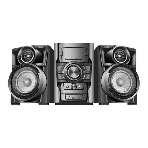
Mini hi-fi system
Hide thumbs
Also See for RAD125:
- Owner's manual (23 pages) ,
- Owner's manual (23 pages) ,
- Owner's manual (23 pages)

Related Manuals for LG RAD125


Summary of Contents for LG RAD125
- Page 1 Internal Use Only Website http://biz.lgservice.com Mini Hi-Fi System SERVICE MANUAL MODEL: RAD125 (RAS125F) P/NO : AFN73250985 JANUARY, 2010...
-
Page 2: Table Of Contents
[CONTENTS] SECTION 1. GENERAL • SERVICING PRECAUTIONS ..........1-2 •... -
Page 3: Section 1. General
SECTION 1. GENERAL SERVICING PRECAUTIONS NOTES REGARDING HANDLING OF THE PICK-UP 1. Notes for transport and storage 1) The pick-up should always be left in its conductive bag until immediately prior to use. 2) The pick-up should never be subjected to external pressure or impact. 2. - Page 4 NOTES REGARDING COMPACT DISC PLAYER REPAIRS 1. Preparations 1) Compact disc players incorporate a great many ICs as well as the pick-up (laser diode). These components are sensitive to, and easily affected by, static electricity. If such static electricity is high voltage, components can be damaged, and for that reason components should be handled with care.
-
Page 5: Esd Precautions
ESD PRECAUTIONS Electrostatically Sensitive Devices (ESD) Some semiconductor (solid state) devices can be damaged easily by static electricity. Such components commonly are called Electrostatically Sensitive Devices (ESD). Examples of typical ESD devices are integrated circuits and some field-effect transistors and semiconductor chip components. The following techniques should be used to help reduce the incidence of component damage caused by static electricity. -
Page 6: Service Information For Eeprom
SERVICE INFORMATION FOR EEPROM POWER ON FLD no disc status Remote control ‘2’ + Front ‘STOP’ DETECT NEW EEPROM push same timing during 5s (OPTION EDIT SCREEN) NAME OPT 0 FLD ‘OP-0…. OPT 1 OPT 2 OPT 3 OPT 4 Move to appropriate position OPT 5 and make changes... -
Page 7: Program Download Guide
PROGRAM DOWNLOAD GUIDE 1. AUDIO PROGRAM Download program file name must be RAD125.HEX If security program (Water Wall) is activated on your PC, you must save the file to the usb storage device and disable the security software, then download the file to your set. - Page 8 2. CD PROGRAM Download program file name must be HB001_DATE_00.BIN If security program (Water Wall) is activated on your PC, you must save the file to the usb storage device and disable the security software, then download the file to your set. Caution: When downloading the file, you should neither unplug the usb device, change to the other function, nor power off the device.
-
Page 9: Specifications
SPECIFICATIONS • GENERAL Power supply Refer to main label Power consumption Refer to main label Net Weight 3.5 kg External dimensions (W x H x D) 202 x 307 x 278 mm Bus Power Supply (USB) DC 5 V 500 mA Operating conditions Temperature 5 °C ~ 35 °C, Operation status: Horizontal... -
Page 10: Section 2. Exploded Views
SECTION 2. EXPLODED VIEWS • CABINET AND MAIN FRAME SECTION (RAD125) NOTES) THE EXCLAMATION POINT WITHIN AN EQUILATERAL TRIANGLE IS INTENDED TO ALERT THE SERVICE PERSONNEL TO THE PRESENCE OF IMPORTANT SAFETY INFORMATION IN SERVICE LITERATURE. 260L FRONT CABLE2 SMPS... -
Page 11: Mechanism Deck Section (Cdm-340)
• MECHANISM DECK SECTION (CDM-340) S P : Non SVC Parts... -
Page 12: Speaker Section
• SPEAKER SECTION 1. FRONT SPEAKER (RAS125F) -
Page 13: Packing Accessory Section
• PACKING ACCESSORY SECTION 910 Battery Cover 824 AM Loop Antenna 801 Instruction Ass'y 825 FM Wire Antenna 808 Battery 900 Remote Control 803 Packing 804 Bag 803 Packing 802 Box... -
Page 14: Section 3. Electrical Part
SECTION 3. ELECTRICAL PART AUDIO ELECTRICAL TROUBLESHOOTIHG GUIDE 1. POWER (SMPS) No .3.7 VA Is the F901 normal? Replace the F901 (Use the same Fuse) Is the BD901 normal? Replace the BD901 Is the TH901(TH902) normal? Replace the TH901 Is Vcc (10 V ~ 18 V) supplied to Is the D904 normal? IC901 Pin7? - Page 15 No .PVDD Is the F901 normal? Replace the F901 (Use the same Fuse) Is the BD901 normal? Replace the BD901 Is the TH901(TH902) normal? Replace the TH901 Is Vcc (10 V ~ 18 V) supplied to Is the D905 normal? IC902 Pin7? Check or Replace the D905 Is the Q910 Base "H"?
- Page 16 No 12 V Is Vcc Check or Replace the D921 (15 V) supplied to Q953 Collector? Is the Check the ‘P.CTL “H” signal 13 V Supplied to Q953 from μ-COM Base? Check or Replace the Q953 No 5 V Is Vcc Check or Replace the D923 (6 V) supplied to IC951 pin1?
-
Page 17: Micom Part Check I
No VFD Check or Replace the D925 Is the D925 normal? Check or Replace the ZD951 Is the ZD951 normal? Is the Q951 normal? Check or Replace the Q951 Check or Replace VFD 2. MICOM PART CHECK I MICOM PART CHECK I Check P-SENS CN105... - Page 18 3. MIOM PART CHECK II MICOM PART CHECK II Check if Refer to SMPS Troubleshooting voltage of CN105 pin10 is 3.7 VA Check Check if output of both end voltage of D105(MBR0540) is 3.7 V D105, 102 Check if IC102_pin49 and Check D105, 102 Replace D105, 102 IC102_pin36,59 are 3.5 V...
-
Page 19: Fld Display Check
5. FLD DISPLAY CHECK FLD DISPLAY CHECK Check CN104 pin1,2,3 voltage Refer to SMPS input Check if both end voltage of F1,F2 are over 3.4 V VKK : over 26 V Check CN304 connection and power Check CN304 connection pin14,15,16(VKK,FL-,FL+), pin11(3.7 VA) Check each pin voltage... - Page 20 6. PWM MODULATION CHECK PWM MODULATION PART CHECK Check CN105 pin10 3.7 VA Refer to SMPS Troubleshooting CN106 pin3 3.3 VA Check IC602(PS9850) VDD pin voltage (16,24,29,32,35,40,48,61,64) 3.3 V Check VDD Core pin voltage (1,21,43,57,59,60) 1.2 V and X602(19.2 MHz) Check Check X602 X602(19.2 MHz)
- Page 21 Check Check IC602(PS9850) CD Assy communication data input Refer to CD Troubleshooting pin4, 5, 6 pin4, 5, 6 PWM wave Check Check each line IC602(PS9850) data resistor output input Check modulator output Check FL: pin31(+),30(-) IC602(PS9850) Replace IC602(PS9850) FR: pin28(+),27(-) other output check...
-
Page 22: Power Amp Part Check
7. POWER AMP PART CHECK POWER AMP PART CHECK Check CN105 pin2: +12 V Refer to SMPS Troubleshooting pin14,15: 20 V Check each IC603 pin27,26,32,35 input voltage Check each IC603 Check each line resistor pin1,22,23,44:+12 V output voltage input Check PWM Modulator input each pin6,8,16,18 Check IC603, pin28,31,36,39 output... - Page 23 8. TUNER/AUX FUNCTION CHECK FUNCTION CHECK Check IC401 (CS5346) pin7,8, Check JK401,TU100 23,24 input Check IC401 Check IC401 Check CN105 pin7: +5 V pin46: +3.3 V (CS5346) pin9 data pin9,10: +3.3 V pin5: +5 V output Check IC401 Check IC401 Check pin6: High IC801(MLC9800)
-
Page 24: Tuner Function Check
9. TUNER FUNCTION CHECK TUNER FUNCTION CHECK Check tuner Check tuner module voltage module(TU100) (pin4: +3.3 V) operation Check IC102 pin21, 22, 23, 24, 25 data in/output Check tuner module data Refer to function check 3-11... - Page 25 CDP TROUBLESHOOTIHG GUIDE 1. CD FUNCTION CD FUNCTION Can the Is MOT_open/close ok? Is load +,- ok? disc insert? (IC301 pin10,11) Check IC301 Is motor ok? Check loading motor (about 12 Ω) Focus/ Check IC301 OPU driving (Focus Disc reading tracking/sled signal (Motor drive IC) and tracking) is ok?
-
Page 26: Usb Function
2. USB FUNCTION USB FUNCTION Plug-in usb device Display “NO USB” Check usb_5V Check CN401 Check usb_D+/D- Display “READ” Check usb jack (JK501) (R501,R502) Display “NO FILE” Check IC801(pin116, 117) Replace IC801 Check usb audio fi le in usb device (MP3, WMA fi... -
Page 27: Details And Waveforms On System Test And Debugging
DETAILS AND WAVEFORMS ON SYSTEM TEST AND DEBUGGING 1. FLASH/SDRAM DATA ADDRESS RESET 2. SERVO 3-14... - Page 28 3. AUDIO PATH LRCK DATA 3-15...
- Page 29 LRCK DATA LRCK DATA 3-16...
- Page 30 USB_5V 3-17...
-
Page 31: Wiring Diagram
WIRING DIAGRAM TUNER MODULE 15PIN 3-18... -
Page 32: Block Diagrams
BLOCK DIAGRAMS 1. MAIN BLOCK DIAGRAM 32.766khz P-SENSE SD; OTW PWM-DAT PWM-CLK PWM-RST DAT, CLK, RST, CE, INT D+/- P-CTRL CD-16M BUSY; SUBSYQ; DOUTA LRCK/ CD-BCK/ DAC-MCLK 9543-RST; CD_R/W CD_MCK/ CD_DIN_DOUT RST, WEN#,CE# 3-19... - Page 33 2. SMPS BLOCK DIAGRAM 3-20...
-
Page 34: Circuit Diagrams
MODIFIED OR ALTERED WITHOUT PERMISSION IMPLEMENTATION OF THE LATEST SAFETY AND during Play mode. FROM THE LG CORPORATION. ALL COMPONENTS PERFORMANCE IMPROVEMENT CHANGES INTO SHOULD BE REPLACED ONLY WITH TYPES IDENTICAL THE SET IS NOT DELAYED UNTIL THE NEW SERVICE TO THOSE IN THE ORIGINAL CIRCUIT. - Page 35 2. MAIN - MICOM CIRCUIT DIAGRAM 3-23 3-24...
- Page 36 3. MAIN - CD DSP & SERVO CIRCUIT DIAGRAM 3-25 3-26...
- Page 37 4. FRONT CIRCUIT DIAGRAM 3-27 3-28...
- Page 38 5. USB CIRCUIT DIAGRAMS 3-29 3-30...
-
Page 39: Circuit Voltage Chart
CIRCUIT VOLTAGE CHART Pin No. Spec. EE Mode (V) Margin Playback Mode (V) Margin Pin No. Spec. EE Mode (V) Margin Playback Mode (V) Margin MAIN BOARD 124 (PLL2VDD12) 1.08~1.32 1.19 0.11 1.18 IC802 SDRAM IC101 EEPROM (M24C16) 1 (VDD) 3.0~3.6 3.34 0.26... - Page 40 PRINTED CIRCUIT BOARD DIARGAMS 1. MAIN P.C. BOARD DIAGRAM ( TOP VIEW ) 3-33 3-34...
- Page 41 MAIN P.C. BOARD DIAGRAM ( BOTTOM VIEW ) 3-35 3-36...
- Page 42 2. SMPS P.C. BOARD DIAGRAM ( TOP VIEW ) 3-37 3-38...
- Page 43 SMPS P.C. BOARD DIAGRAM ( BOTTOM VIEW ) Warning Parts that are shaded are critical with respect to risk of fire or electrical shock. 3-39 3-40...
- Page 44 3. FRONT & USB P.C. BOARD DIAGRAM ( TOP VIEW ) 3-41 3-42...
- Page 45 FRONT & USB P.C. BOARD DIAGRAM ( BOTTOM VIEW ) 3-43 3-44...
Need help?
Do you have a question about the RAD125 and is the answer not in the manual?
Questions and answers