Table of Contents
Advertisement
SERVICE MANUAL
Ver 1.2 2004.08
CX-JV4 is the tuner, amplifier, cassette deck and
disc player section in JAX-V4.
TUNER
FM tuning range
87.5 MHz to 108 MHz
FM usable sensitivity (IHF)
13.2 dBf
FM antenna terminal
75 ohms (unbalanced)
AM tuning range
Middle Eastern model:
531 kHz to 1602 kHz (9 kHz step)
Other models:
530 kHz to 1710 kHz (10 kHz step)
531 kHz to 1602 kHz (9 kHz step)
350 µV/m
AM usable sensitivity
AM antenna
Loop antenna
AMPLIFIER
Power output
Rated: 80 W + 80 W (1 kHz, T.H.D.
1 %, 6 ohms)
Reference: 100 W + 100 W (1 kHz,
T.H.D. 10 %, 6 ohms)
Total harmonic distortion
0.08 % (20 W, 1 kHz, 6 ohms, DIN
AUDIO)
Input
VIDEO/AUX: 1.2 V
Outputs
FRONT SPEAKER: 6 ohms or more
SURROUND SPEAKER (JAX-V5
only): 8 ohms or more
PHONES: 32 ohms or more
REC OUT: 0.775 V
VIDEO OUT: 1 Vp-p (75 ohms)
CASSETTE DECK
Track format
4 tracks, 2 channels stereo
Frequency response
50 Hz – 8 kHz
Recording system
AC bias
Heads
Deck A: playback x 1
Deck B: Recording/playback x 1,
erase x 1
Sony Corporation
9-961-182-03
2004H05-1
Personal Audio Company
© 2004.08
Published by Sony Engineering Corporation
Model Name Using Similar Mechanism
CD Mechanism Type
CD
Section
Base Unit Name
Optical Pick-up Name
Model Name Using Similar Mechanism
Tape deck
Section
Tape Transport Mechanism Type
SPECIFICATIONS
DISC PLAYER
Laser
D/A converter
Signal-to-noise ratio
Harmonic distortion
Video signal
Video data
Audio data
GENERAL
Power requirements
Power consumption
Power consumption
in standby mode
Dimensions (W x H x D)
Weight
Specifications and external appearance are subject to change
without notice.
COPYRIGHT
Check copyright laws relevant to recordings from discs, tuner
or tape for the country where the unit is to be used.
Licensed by BBE Sound, Inc. under USP4638258, 5510752
and 5736897.
CX-JV4
CX-JV5
CDM74B-30BD61S
BU-30BD61S
OP Assy (A-MAX.3)
CX-JV5
CWM43FR16
Semiconductor laser (λ = 795 nm)
Emission duration:
continuous
1 bit dual
90 dB (1 kHz, 0 dB)
0.05 % (1 kHz, 0 dB)
NTSC/PAL color system (selectable)
MPEG1
MPEG1, Layer2 (VIDEO CD)
MPEG1, Layer3 (MP3-CD)
110-120 V/220-240 V AC (Switchable),
50 Hz/60 Hz
130 W
With ECO mode on: 0.25 W
With ECO mode off: 25 W
280 x 330 x 392.5 mm
8.1 kg
COMPACT DISC DECK RECEIVER
E Model
Advertisement
Table of Contents

Subscribe to Our Youtube Channel
Related Manuals for Aiwa CX-JV4


Summary of Contents for Aiwa CX-JV4
-
Page 1: Specifications
CX-JV4 SERVICE MANUAL E Model Ver 1.2 2004.08 CX-JV4 is the tuner, amplifier, cassette deck and disc player section in JAX-V4. Model Name Using Similar Mechanism CX-JV5 CD Mechanism Type CDM74B-30BD61S Section Base Unit Name BU-30BD61S Optical Pick-up Name OP Assy (A-MAX.3) - Page 2 LINE WITH MARK 0 ON THE SCHEMATIC DIAGRAMS AND IN THE PARTS LIST ARE CRITICAL TO SAFE OPERATION. REPLACE THESE COMPONENTS WITH SONY PARTS WHOSE PART NUMBERS APPEAR AS SHOWN IN THIS MANUAL OR IN SUPPLEMENTS PUB- LISHED BY SONY.
-
Page 3: Table Of Contents
CX-JV4 TABLE OF CONTENTS SERVICING NOTES EXPLODED VIEWS ..........4 7-1. Case Section ..............60 GENERAL 7-2. Front Panel Section-1 ............61 7-3. Front Panel Section-2 ............62 Location of Controls ............7 7-4. Front Panel Section-3 ............63 7-5. Front Panel Section-4 ............64 DISASSEMBLY 7-6. -
Page 4: Servicing Notes
CX-JV4 SECTION 1 SERVICING NOTES RELEASING THE DISC TRAY LOCK NOTES ON HANDLING THE OPTICAL PICK-UP The disc tray lock function for the antitheft of an demonstration BLOCK OR BASE UNIT disc in the store is equipped. The laser diode in the optical pick-up block may suffer electro-... - Page 5 CX-JV4 HOW TO OPEN THE DISC TRAY WHEN POWER SWITCH TURNS OFF. 1 Remove the case (side-L). 2 Turn the loading gear in the direction of arrow A . 3 Pull-out the disc tray.
- Page 6 CX-JV4 SERVICE POSITION – CD mechanism deck – VMP50 board (CN801) main board (CN691) Connect wire (flat type) (19 core) to main board (CN691) and VMP50 board (CN801). – Tape mechanism deck – panel board (CN601) main board (CN301) Connect wire (flat type) (13 core) to...
-
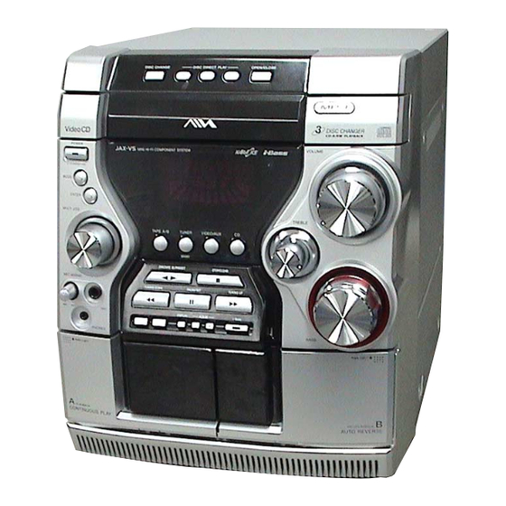
Page 7: General
CX-JV4 SECTION 2 This section is extracted from instruction manual. GENERAL • LOCATION OF CONTROLS 5 MULTI JOG @ Remote sensor When used in combination with ENTER and MULTI JOG, Receives a signal from the remote. Refer to the pages indicated in parentheses for details. - Page 8 CX-JV4 8 SHIFT PLAY MODE Hold down when pressing a numbered button to change CD: selects Shuffle, Programmed playback, etc. Refer to the pages indicated in parentheses for details. its function to that printed above the number. Tape: selects a reverse mode (deck B only) e.g.)
-
Page 9: Disassembly
CX-JV4 SECTION 3 DISASSEMBLY • This set can be disassembled in the order shown below. 3-1. DISASSEMBLY FLOW Note 1: The process described in can be performed in any order. Note 2: Without completing the process described in , the next process can not be performed. -
Page 10: Case (Side-L/R)
CX-JV4 Note: Follow the disassembly procedure in the numerical order given. 3-2. CASE (SIDE-L/R) 2 two screws 5 case (side-L) × (BVTP3 1 two case screws 2 two screws × (BVTP3 1 two case screws 1 case screw 5 case (side-R) 1 case screw 3-3. -
Page 11: Tray Panel
CX-JV4 3-4. TRAY PANEL 1 Turn the loading gear in the direction of arrow A . 2 Pull-out the disc table. 3 four claws 4 tray panel 3-5. CD MECHANISM DECK (CDM74B-30BD61S) 5 CD mechanism deck (CDM74B-30BD61S) 1 wire (flat type) -
Page 12: Front Panel Section
CX-JV4 3-6. FRONT PANEL SECTION 8 headphone board 1 wire (flat type) (11 core) 7 screw (CN694) (BVWHTP) 2 connector (CN302) 6 connector (CN601) 3 connector (CN301) 9 front panel section 4 three screws × (BVTP3 3-7. MECHANICAL DECK (CWM43FR16) -
Page 13: Rear Cabinet Section
CX-JV4 3-8. REAR CABINET SECTION 4 rear cabinet section 2 connector (CN504) 1 wire (flat type) (11 core) (CN801) 3 three screws × (BVTP3 3 screw × (BVTP3 3-9. PT BOARD, MAIN BOARD 6 screw × (BVTT3 8 Remove the PWB PT HLDR in the direction of the arrow. -
Page 14: Table Assy
CX-JV4 3-10. TABLE ASSY 5 two claws 4 hook 3 wire (flat type) (5 core) (CN702) 1 Turn the loading gear 2 Pull-out the table assy. in the direction of arrow A . 6 table assy 3-11. MOTOR (TB) BOARD 1 screw (PTPWH M2.6) -
Page 15: Motor (Ld) Board
CX-JV4 3-12. MOTOR (LD) BOARD 3 two screws (BTTP M2.6) 4 motor (LD) board 2 connector (CN704) 1 belt (loading) 3-13. BASE UNIT (BU-30BD61S) 9 base unit (BU-30BD61S) 1 wire (flat type) (23 core) (CN102) 1 wire (flat type) (9 core) -
Page 16: Bd Board
CX-JV4 3-14. BD BOARD BU-30BD61S assy 1 wire (flat type) (16 core) (CN101) 2 Remove two solders. 3 Remove two solders. 4 BD board... -
Page 17: Test Mode
CX-JV4 SECTION 4 TEST MODE [COLD RESET] [CHANGE-OVER OF AM TUNER STEP BETWEEN • The cold reset clears all data including preset data stored in the 9 kHz AND 10 kHz] RAM to initial conditions. Execute this mode when returning •... -
Page 18: Electrical Adjustments
CX-JV4 SECTION 5 ELECTRICAL ADJUSTMENTS RFDC signal waveform CD SECTION VOLT/DIV: 200 mV TIME/DIV: 500 ns Note: 1. Use YEDS-18 disc (3-702-101-01) unless otherwise indicated. 2. Use an oscilloscope with more than 10MΩ impedance. 3. Clean the object lens by an applicator with neutral detergent when the level: 0.6 ±... - Page 19 CX-JV4 E-F BALANCE (1 TRACK JUMP) ADJUSTMENT Adjustment and Connecting Location: Connection: – BD BOARD (Conductor Side) – oscilloscope BD board TP (TE) TP (VC) — Procedure: Connect an oscilloscpe to test point TP (TE) and TP (VC) on the BD board.
- Page 20 CX-JV4 MEMO...
-
Page 21: Diagrams
CX-JV4 SECTION 6 DIAGRAMS 6-1. BLOCK DIAGRAM – CD SERVO Section – FILTER XTSL RF AMP, DIGITAL SIGNAL PROCESSOR FOCUS/TRACKING ERROR AMP IC101 (1/2) 53 55 52 54 XTAO IC103 DETECTOR +3.3V (CD) X201 CLOCK XTAI 16.9344MHz GENERATOR DATA, BCK, LRCK... -
Page 22: Block Diagram - Audio/Video Section
CX-JV4 6-2. BLOCK DIAGRAM – AUDIO/VIDEO Section – DATAI, DATAO, ACK, STB DATAI AUX7 (Page 23) AUX2 AUX6 MPEG VIDEO/AUDIO DECODER IC802 (2/2) AUX15 DATA, BCK, LRCK DATA (Page 21) TDMDP AOUT/SELPLL0 21 TSD AOL+ MIX AMP (Page 24) TDMCLK... -
Page 23: Block Diagram - Tuner/Tape/Panel Section
CX-JV4 6-3. BLOCK DIAGRAM – TUNER/TAPE/PANEL Section – PB SWITCH (Page 24) L-CH Q301 (PB) (DECK-A) R-CH R-CH FM/AM TUNER PACK FM 75Ω L-CH (Page 24) FM ANT (COAXIAL) PB SWITCH R-CH R-CH Q303 L-CH AM LOOP AM ANT MUTING... -
Page 24: Block Diagram - Amp/Power Supply Section
CX-JV4 6-4. BLOCK DIAGRAM – AMP/POWER SUPPLY Section – DATA, CLK, LATCH LEVEL SHIFT DATA (Page 23) Q406, 407 VOCAL FADER ON/OFF SWITCH IC712 DIGITAL ECHO DATA MIC LEVEL IC402 LEVEL SHIFT Q402, 403 Q401 REC AMP LATCH J603 (2/2) -
Page 25: Note For Printed Wiring Boards And Schematic Diagrams
CX-JV4 6-5. NOTE FOR PRINTED WIRING BOARDS AND SCHEMATIC DIAGRAMS • Circuit Boards Location Note on Printed Wiring Board: Note on Schematic Diagram: • All capacitors are in µF unless otherwise noted. pF: µµF • X : parts extracted from the component side. -
Page 26: Printed Wiring Board - Bd Section
CX-JV4 6-6. PRINTED WIRING BOARD – BD Section – • See page 25 for Circuit Boards Location. :Uses unleaded solder. BD BOARD (COMPONENT SIDE) – BD BOARD (CONDUCTOR SIDE) M101 (SPINDLE) C272 R285 C277 R308 C226 C211 C212 R204 R260... -
Page 27: Schematic Diagram - Bd Section
CX-JV4 6-7. SCHEMATIC DIAGRAM – BD Section – • • See page 46 for Waveforms. See page 47 for IC Block Diagrams. R111 150k C116 (RFACI) RFAC C213 3300p RFSW C112 RF AMP, C109 FOCUS/TRACKING R311 ERROR AMP C119 R104... -
Page 28: Printed Wiring Boards - Changer Section
CX-JV4 6-8. PRINTED WIRING BOARDS – CHANGER Section – • See page 25 for Circuit Boards Location. :Uses unleaded solder. SENSOR BOARD SW BOARD CN751 IC731 S751 MAIN BOARD OPEN/CLOSE CN692 DETECT (Page 33) DRIVER BOARD CLOSE C715 OPEN Q731... -
Page 29: Schematic Diagram - Changer Section
CX-JV4 6-9. SCHEMATIC DIAGRAM – CHANGER Section – • See page 47 for IC Block Diagrams. LOADING MOTOR DRIVE IC701 BA6956AN R702 R701 CN721 CN704 LM-2 LM-2 D701 M751 C751 LM-1 LM-1 MTZJ-T-77 0.01 (LOADING) 5.1A S711 DISC TRAY ADDRESS DETECT... -
Page 30: Schematic Diagram - Vmp Section (1/2)
CX-JV4 6-10. SCHEMATIC DIAGRAM – VMP Section (1/2) – • See page 46 for Waveforms. • See page 47 for IC Block Diagram. (1/2) R802 R801 4.7k 4.7k C830 R837 C822 C802 LA12 AUX4 C801 LA13 R877 R858 LA14 LA14... -
Page 31: Schematic Diagram - Vmp Section (2/2)
CX-JV4 6-11. SCHEMATIC DIAGRAM – VMP Section (2/2) – • See page 46 for Waveforms. CN801 (2/2) R841 I-CD DATA R906 JR802 1.5K R842 O-CD ACK R909 JR803 1.5K R843 O-CD DATA R844 I-CD STB R950 R951 4.7k 4.7k C715... -
Page 32: Printed Wiring Board - Vmp Section
CX-JV4 6-12. PRINTED WIRING BOARD – VMP Section – • See page 25 for Circuit Boards Location. :Uses unleaded solder. • Semiconductor Location J901 – VMP Section – VMP50 BOARD VIDEO OUT VMP50 BOARD (COMPONENT SIDE) (CONDUCTOR SIDE) Ref. No. -
Page 33: Printed Wiring Boards - Main Section
CX-JV4 6-13. PRINTED WIRING BOARDS – MAIN Section – • See page 25 for Circuit Boards Location. :Uses unleaded solder. MAIN BOARD VMP50 JW802 BOARD JW661 CN801 JW803 (Page 32) JW662 JW611 JW610 JW609 JW618 JW616 JW805 JW804 JW663 C653... -
Page 34: Schematic Diagram - Main Section (1/4)
CX-JV4 6-14. SCHEMATIC DIAGRAM – MAIN Section (1/4) – (1/4) Q001 CN001 R020 2SB1370 WH013 R017 D019 B+ SWITCH 0.22 EGP20D VM(AC) VM(AC) C007 D020 VH(AC) 3300 D021 D022 EGP20D EGP20D EGP20D VH(AC) C011 C012 C033 VL(AC) VL(AC) GND(M) FIL-1... -
Page 35: Schematic Diagram - Main Section (2/4)
CX-JV4 6-15. SCHEMATIC DIAGRAM – MAIN Section (2/4) – D107 (2/4) R123 Q101,103 R131 Q186 MC2838 6.8k 4.7k 2SA1235 PRE DRIVE R119 2.2k R117 R121 C105 Q127 C181 2.2k D105 FN1016 R183 R193 MC2836 3.9k FINAL DRIVE Q103 R133 C121... -
Page 36: Schematic Diagram - Main Section (3/4)
CX-JV4 6-16. SCHEMATIC DIAGRAM – MAIN Section (3/4) – • See page 46 for Waveforms. • See page 47 for IC Block Diagram. (3/4) SP-A-GND C687 0.01 TU/AUX-A-GND CD-A-GND FR-A-GND FUNC-A-GND CD-D-GND R749 R772 R771 R746 R750 R741 R745 R757 3.9k... -
Page 37: Schematic Diagram - Main Section (4/4)
CX-JV4 6-17. SCHEMATIC DIAGRAM – MAIN Section (4/4) – • See page 47 for IC Block Diagrams. (4/4) R687 R676 R677 R678 4.7k 2.2k C679 CN801 R674 R675 3.3k 3.3k C677 0.33 Q671 Q672 Q673 R679 DATA 2SK2158 2SK2158 2SK2158... -
Page 38: Printed Wiring Boards - Vf/Hp Section
CX-JV4 6-18. PRINTED WIRING BOARDS – VF/HP Section – • :Uses unleaded solder. See page 25 for Circuit Boards Location. MAIN BOARD WH201 VF BOARD (Page 33) MAIN BOARD CN710 (Page 33) CN711 WH230 JR708 HEADPHONE JW714 JR704 BOARD R715... -
Page 39: Schematic Diagram - Vf/Hp Section
CX-JV4 6-19. SCHEMATIC DIAGRAM – VF/HP Section – • See page 47 for IC Block Diagram. C718 0.22 R722 C717 0.22 FB221 R721 WH230 JW224 J221 PHONES R-OUT R-IN L-IN IC712 L OUT R222 R221 BU4052BCF 2.2k 2.2k (Page 35) -
Page 40: Printed Wiring Board - Panel Section
CX-JV4 6-20. PRINTED WIRING BOARD – PANEL Section – • See page 25 for Circuit Boards Location. :Uses unleaded solder. R906 C909 R908 R907 R927 R932 D623 D622 C907 C906 C908 R905 C905 IC801 D620 D621 MAIN BOARD CN694 R903... -
Page 41: Schematic Diagram - Panel Section
CX-JV4 6-21. SCHEMATIC DIAGRAM – PANEL Section – • • See page 46 for Waveforms. See page 47 for IC Block Diagram. FL901 FLUORESCENT INDICATOR TUBE JW902 R943 R942 1.8k 1.8k JW901 C916 C917 R944 6.8k JR903 D201 R221 CN701... -
Page 42: Printed Wiring Boards - Key Section
CX-JV4 6-22. PRINTED WIRING BOARDS – KEY Section – • See page 25 for Circuit Boards Location. :Uses unleaded solder. • Semiconductor KEY BOARD Location LED901 STANDBY/ON Ref. No. Location D401 D403 IC401 S315 IC402 POWER LED201 LED901 A-10 Q401... -
Page 43: Schematic Diagram - Key Section
CX-JV4 6-23. SCHEMATIC DIAGRAM – KEY Section – • See page 47 for IC Block Diagram. R801 R803 R809 R811 S801 S803 VOLUME TREBLE R802 C801 C802 R804 R810 C805 C806 R812 1000p 1000p 1000p 1000p R301 R302 R303 R304... -
Page 44: Printed Wiring Board - Pt Section
CX-JV4 6-24. PRINTED WIRING BOARD – PT Section – • See page 25 for Circuit Boards Location. :Uses unleaded solder. PT BOARD (AC IN) CN090 JW017 PT002 POWER TRANSFORMER D002 D003 (SUB) PT003 POWER TRANSFORMER (MAIN) CN093 S001 S001 VOLTAGE... -
Page 45: Schematic Diagram - Pt Section
CX-JV4 6-25. SCHEMATIC DIAGRAM – PT Section – PT003 POWER TRANSFORMER CN093 (MAIN) VM(AC) VM(AC) VH(AC) VH(AC) VL(AC) VL(AC) S001 GND(M) VOLTAGE SELECTOR FIL-1 100-120V ∗ (Page 34) FIL-2 220-240V P-ON C003 VSTBY 0.01 ∗ NOT REPLACEABLE: BUILT IN TRANSFORMER... - Page 46 CX-JV4 • Waveforms – MAIN Board – – BD Board – – VMP50 Board – – KEY Board – 1 IC103 qg (RFAC) (CD Play Mode) rd IC801 rs (CPUCLK) (Video CD Play Mode) rk IC801 ok (TDMFS) (Video CD Play Mode)
- Page 47 CX-JV4 • IC Block Diagrams – BD Board – IC101 CXD3068Q 59 58 57 56 55 54 53 52 51 50 49 48 47 46 45 44 43 42 41 DVDD2 ASYE DIGITAL ASYMMETRY CORRECTOR DIGITAL DOUT LRCK D/A DIGITAL...
- Page 48 CX-JV4 IC102 AN41020A PVCC/2 DIRECTION DETECTION DIRECTION DETECTION DIRECTION DETECTION PVCC/2 DIRECTION DETECTION RESET CIRCUIT . STANDBY . BAND-GAP . SVCC...
- Page 49 CX-JV4 IC103 CXA2647N-T4 ROM/RW DC OFST RFDCI – – RFDC – ROM/RW VOFST APC AMP RF OFF AT VCC RFAC EQ IN ROM/RW RFAC AC SUM SUMMING VOFST – – ROM/RW TE BAL ROM/RW – VOFST – – DVC OR Hi-Z...
-
Page 50: Main Board
CX-JV4 – MAIN Board – IC601 BD3881FV BASS BASS VOLUME TREBLE LOGIC CONTROL VOLUME TREBLE IC671 NJM2156M (TE2) IC672 BU2092F-E2 16 15 14 13 12 11 19 18 17 16 12 11 12 BIT BIAS CONTROL SHIFT CIRCUIT REGISTER OUTPUT... -
Page 51: Panel Board
CX-JV4 – VF Board – – PANEL Board – IC712 BU4052BCF-E2 IC501 MM1614A 2XCOM CURRENT BIAS LIMITTER XCOM REFERENCE – DRIVER THERMAL SHUTDOWN – KEY Board – IC402 BU9262AFS N. C. DLYVOL 32 MIXIN TESTB LOGIC INPUT 31 MICIN CONTROL... -
Page 52: Ic Pin Function Description
CX-JV4 6-26. IC PIN FUNCTION DESCRIPTION • BD BOARD IC101 CXD3068Q (DIGITAL SIGNAL PROCESSOR, DIGITAL SERVO PROCESSOR) Pin No. Pin Name Description DVDD0 — Power supply terminal (+3.3V) (digital system) XRST Reset signal input from the MPEG video/audio decoder “L”: reset MUTE Muting on/off control signal input terminal “H”: muting on Not used... - Page 53 CX-JV4 Pin No. Pin Name Description AVDD0 — Power supply terminal (+3.3V) (analog system) ASYO EFM full-swing output terminal ASYI Asymmetry comparator voltage input terminal RFAC EFM signal input from the RF amplifier AVSS1 — Ground terminal (analog system) CLTV...
- Page 54 CX-JV4 • VMP50 BOARD IC801 ES3880FM (VIDEO CD MPEG PROCESSOR) Pin No. Pin Name Description VDD3 — Power supply terminal (+3.3V) Row address strobe signal output to the D-RAM Write enable signal output to the D-RAM 4 to 12 MA0 to MA8...
- Page 55 CX-JV4 Pin No. Pin Name Description BCLK Bit clock signal (2.8224 MHz) input from the digital signal processor PCMD Serial data input from the digital signal processor LRCK L/R sampling clock signal (44.1 kHz) input from the digital signal processor Column address strobe signal output to the D-RAM —...
- Page 56 CX-JV4 • VMP50 BOARD IC802 ES3889 (MPEG VIDEO/AUDIO DECODER) Pin No. Pin Name Description 1, 2 — Ground terminal — Not used 4, 5 — Power supply terminal (+5V) DSC-C Clock signal input from the video CD MPEG processor AUX00 Video system select switch input terminal “L”: PAL, “H”: AUTO or NTSC...
- Page 57 CX-JV4 Pin No. Pin Name Description AOL– Audio data (L-ch) output to the electrical volume 49, 50 MIC2, MIC1 MIC signal input terminal Not used AGND — Ground terminal (analog system) VREF Not used Not used RSET Not used COMP...
- Page 58 CX-JV4 • PANEL BOARD IC901 LC876764C-52M9-E (SYSTEM CONTROLLER) Pin No. Pin Name Description SYS-MUTE Line muting on/off control signal output terminal LATCH (ECHO) Serial data latch pulse signal output to the digital echo TU/EVOL DO Serial data output to the FM/AM tuner unit, motor/plunger driver and electrical volume...
- Page 59 CX-JV4 Pin No. Pin Name Description Deck-A mode detection signal input and segment drive signal output to the fluorescent indicator A MODE/S13 tube 56 to 71 S14 to S29 Segment drive signal output to the fluorescent indicator tube VDD4 —...
-
Page 60: Exploded Views
CX-JV4 SECTION 7 EXPLODED VIEWS NOTE: • -XX and -X mean standardized parts, so they • Items marked “*” are not stocked since they The components identified by may have some difference from the original are seldom required for routine service. Some mark 0 or dotted line with mark one. -
Page 61: Front Panel Section-1
CX-JV4 7-2. FRONT PANEL SECTION-1 not supplied not supplied not supplied front panel section -2 Ref. No. Part No. Description Remark Ref. No. Part No. Description Remark 4-245-178-01 PLATING, KNOB ROTARY (JOG) 4-245-176-01 PLATING, KNOB ROTARY (BASS) 4-245-180-01 PLATING, KNOB ROTARY (TRE) -
Page 62: Front Panel Section-2
CX-JV4 7-3. FRONT PANEL SECTION-2 front panel section -3 Ref. No. Part No. Description Remark Ref. No. Part No. Description Remark 1-688-379-11 CD KEY BOARD 1-769-857-11 WIRE (FLAT TYPE) (5 CORE) 1-688-400-14 HEADPHONE BOARD A-4748-123-A KEY BOARD, COMPLETE 3-229-336-01 SCREW, +BVWH TAPPING... -
Page 63: Front Panel Section-3
CX-JV4 7-4. FRONT PANEL SECTION-3 front panel section -4 Ref. No. Part No. Description Remark Ref. No. Part No. Description Remark 4-245-193-01 RING (BASS) 4-245-164-01 GUIDE (BASS) 4-249-033-31 WINDOW (VCD), DISPLAY X-4955-560-1 KEY ASSY (POWER) 4-233-980-01 RUBBER FOOT X-4955-846-1 KEY ASSY, VCD (m. X. M. SYNC DUB. -
Page 64: Front Panel Section-4
CX-JV4 7-5. FRONT PANEL SECTION-4 Ref. No. Part No. Description Remark Ref. No. Part No. Description Remark 4-245-198-01 WINDOW (2), CASSETTE 4-245-153-71 CABINET, FRONT 4-245-160-11 BOX (2), CASSETTE 4-231-836-01 SPRING (HEART CAM-A) 4-245-196-01 SPRING (BOX CASS R), TORSION 4-231-841-01 SPRING (HEART CAM-B) -
Page 65: Chassis Section
CX-JV4 7-6. CHASSIS SECTION M501 not supplied not supplied not supplied (TR board) PT003 not supplied not supplied not supplied not supplied not supplied not supplied not supplied not supplied The components identified by mark 0 or dotted line with mark 0 are critical for safety. -
Page 66: Cd Mechanism Deck Section-1 (Cdm74-30Bd61S)
CX-JV4 7-7. CD MECHANISM DECK SECTION-1 (CDM74B-30BD61S) M741 CD mechanism deck section -2 Ref. No. Part No. Description Remark Ref. No. Part No. Description Remark 4-243-815-01 TABLE (LOADING) 1-687-134-11 MOTOR (TB) BOARD 4-218-252-61 SCREW (+PTPWH M2.6), FLOATING 4-243-816-01 TRAY 4-218-253-21 SCREW (M2.6), +BTTP... -
Page 67: Cd Mechanism Deck Section-2 (Cdm74-30Bd61S)
CX-JV4 7-8. CD MECHANISM DECK SECTION-2 (CDM74B-30BD61S) S711 M751 CD mechanism deck section -3 Ref. No. Part No. Description Remark Ref. No. Part No. Description Remark 4-244-108-01 GEAR, SWING 4-218-252-61 SCREW (+PTPWH M2.6), FLOATING 4-244-034-01 BELT (LOADING) 4-224-608-01 COLLAR, SWING... -
Page 68: Cd Mechanism Deck Section-3 (Cdm74-30Bd61S)
CX-JV4 7-9. CD MECHANISM DECK SECTION-3 (CDM74B-30BD61S) not supplied BU-30BD61S Ref. No. Part No. Description Remark Ref. No. Part No. Description Remark X-4955-756-1 PULLEY (A) ASSY, CHUCKING 4-231-451-01 INSULATOR (BU-30) 4-228-414-01 BRACKET (YOKE) 4-227-045-11 SPRING (INSULATOR), COIL 4-231-513-01 PULLEY (B) (BU-30), CHUCKING 4-231-151-01 STOPPER (BU) 4-218-252-61 SCREW (+PTPWH M2.6), FLOATING... -
Page 69: Base Unit Section (Bu-30Bd61S)
CX-JV4 7-10. BASE UNIT SECTION (BU-30BD61S) The components identified by mark 0 or dotted line with mark 0 are critical for safety. Replace only with part number specified. Ref. No. Part No. Description Remark Ref. No. Part No. Description Remark... -
Page 70: Electrical Parts List
CX-JV4 SECTION 8 ELECTRICAL PARTS LIST NOTE: • Due to standardization, replacements in the • Items marked “*” are not stocked since they The components identified by mark 0 or dotted line with mark parts list may be different from the parts speci- are seldom required for routine service. - Page 71 CX-JV4 CD KEY DRIVER Ref. No. Part No. Description Remark Ref. No. Part No. Description Remark R102 1-216-835-11 METAL CHIP 1/10W R291 1-216-864-11 SHORT CHIP R103 1-216-845-11 METAL CHIP 100K 1/10W R104 1-216-835-11 METAL CHIP 1/10W R303 1-216-864-11 SHORT CHIP...
- Page 72 CX-JV4 DRIVER HEADPHONE Ref. No. Part No. Description Remark Ref. No. Part No. Description Remark C405 1-126-960-11 ELECT < DIODE > C406 1-126-934-11 ELECT 220uF D701 8-719-921-42 DIODE MTZJ-5.1A C407 1-162-926-11 CERAMIC CHIP 82PF D711 8-719-109-69 DIODE RD3.6ESB2 C408 1-126-956-11 ELECT 0.1uF...
- Page 73 CX-JV4 Ref. No. Part No. Description Remark Ref. No. Part No. Description Remark JR403 1-216-864-11 SHORT CHIP R424 1-216-846-11 METAL CHIP 120K 1/10W JR404 1-216-864-11 SHORT CHIP R425 1-216-864-11 SHORT CHIP R429 1-216-841-11 METAL CHIP 1/10W < COIL > R430...
- Page 74 CX-JV4 MAIN Ref. No. Part No. Description Remark Ref. No. Part No. Description Remark < VARIABLE RESISTOR > C202 1-165-621-11 CERAMIC CHIP 0.1uF VR401 1-227-502-11 RES, VAR, CARBON 10K (MIC MIXING) C203 1-165-621-11 CERAMIC CHIP 0.1uF C204 1-165-621-11 CERAMIC CHIP 0.1uF...
- Page 75 CX-JV4 MAIN Ref. No. Part No. Description Remark Ref. No. Part No. Description Remark C661 1-126-934-11 ELECT 220uF C662 1-126-947-11 ELECT 47uF D045 8-719-083-71 DIODE UDZS-TE1730B C663 1-164-156-11 CERAMIC CHIP 0.1uF D063 6-500-334-01 DIODE MC2836 D064 6-500-335-01 DIODE MC2838 C664 1-164-156-11 CERAMIC CHIP 0.1uF...
- Page 76 CX-JV4 MAIN Ref. No. Part No. Description Remark Ref. No. Part No. Description Remark IC601 6-702-895-01 IC BD3881FV Q104 6-550-316-01 TRANSISTOR 2SB0792A0LS0 IC671 6-704-074-01 IC NJM2156M (TE2) Q105 8-729-120-28 TRANSISTOR 2SC1623-L5L6 IC672 8-759-396-78 IC BU2092F-E2 Q106 8-729-120-28 TRANSISTOR 2SC1623-L5L6 Q107...
- Page 77 CX-JV4 MAIN Ref. No. Part No. Description Remark Ref. No. Part No. Description Remark Q677 8-729-045-62 FET 2SK2158-T2B Q741 8-729-120-28 TRANSISTOR 2SC1623-L5L6 R083 1-216-840-11 METAL CHIP 1/10W Q742 8-729-120-28 TRANSISTOR 2SC1623-L5L6 R084 1-216-844-11 METAL CHIP 1/10W Q743 8-729-052-79 TRANSISTOR 2SD1306NETL...
- Page 78 CX-JV4 MAIN Ref. No. Part No. Description Remark Ref. No. Part No. Description Remark R157 1-216-809-11 METAL CHIP 1/10W R158 1-216-809-11 METAL CHIP 1/10W R284 1-216-827-11 METAL CHIP 3.3K 1/10W R159 1-216-073-00 RES-CHIP 1/10W R290 1-216-841-11 METAL CHIP 1/10W R291 1-216-825-11 METAL CHIP 2.2K...
- Page 79 CX-JV4 MAIN Ref. No. Part No. Description Remark Ref. No. Part No. Description Remark R629 1-216-833-11 METAL CHIP 1/10W R630 1-216-833-11 METAL CHIP 1/10W R702 1-216-833-11 METAL CHIP 1/10W R631 1-216-825-11 METAL CHIP 2.2K 1/10W R703 1-216-833-11 METAL CHIP 1/10W...
- Page 80 CX-JV4 MOTOR (LD) MOTOR (TB) PANEL Ref. No. Part No. Description Remark Ref. No. Part No. Description Remark 1-687-133-11 MOTOR (LD) BOARD C920 1-162-919-11 CERAMIC CHIP 22PF C921 1-164-156-11 CERAMIC CHIP 0.1uF ***************** C922 1-162-919-11 CERAMIC CHIP 22PF ************************************************************ C923...
- Page 81 CX-JV4 PANEL Ref. No. Part No. Description Remark Ref. No. Part No. Description Remark JR202 1-216-864-11 SHORT CHIP R108 1-249-417-11 CARBON 1/4W JR203 1-216-864-11 SHORT CHIP R109 1-249-417-11 CARBON 1/4W JR204 1-216-864-11 SHORT CHIP R110 1-249-417-11 CARBON 1/4W JR205 1-216-864-11 SHORT CHIP...
- Page 82 CX-JV4 PANEL Ref. No. Part No. Description Remark Ref. No. Part No. Description Remark R501 1-249-408-11 CARBON 1/4W R919 1-216-845-11 METAL CHIP 100K 1/10W R502 1-216-841-11 METAL CHIP 1/10W R503 1-216-841-11 METAL CHIP 1/10W R920 1-216-845-11 METAL CHIP 100K 1/10W...
- Page 83 CX-JV4 Ver 1.2 PANEL SENSOR VMP50 Ref. No. Part No. Description Remark Ref. No. Part No. Description Remark X902 1-795-880-11 VIBRATOR, CERAMIC (8.64MHz) 1-688-401-14 VF BOARD ************************************************************ ******** 1-688-763-11 PT BOARD < CAPACITOR > ********* < CAPACITOR > C711 1-165-176-11 CERAMIC CHIP 0.047uF...
- Page 84 CX-JV4 VMP50 Ref. No. Part No. Description Remark Ref. No. Part No. Description Remark C843 1-162-919-11 CERAMIC CHIP 22PF C703 1-164-346-11 CERAMIC CHIP C844 1-162-919-11 CERAMIC CHIP 22PF C704 1-164-346-11 CERAMIC CHIP C846 1-162-919-11 CERAMIC CHIP 22PF C705 1-162-968-11 CERAMIC CHIP 0.0047uF 10%...
- Page 85 CX-JV4 VMP50 Ref. No. Part No. Description Remark Ref. No. Part No. Description Remark JR804 1-216-296-11 SHORT CHIP R722 1-218-917-11 METAL CHIP 820K 0.5% 1/10W R801 1-216-829-11 METAL CHIP 4.7K 1/10W < COIL > R802 1-216-829-11 METAL CHIP 4.7K 1/10W...
- Page 86 CX-JV4 VMP50 Ref. No. Part No. Description Remark Ref. No. Part No. Description Remark R874 1-216-809-11 METAL CHIP 1/10W R939 1-216-809-11 METAL CHIP 1/10W R940 1-216-809-11 METAL CHIP 1/10W R875 1-216-809-11 METAL CHIP 1/10W R941 1-216-809-11 METAL CHIP 1/10W R876...
- Page 87 CX-JV4 CX-JV4 DIAGRAMS 1-1. NOTE FOR PRINTED WIRING BOARDS AND SCHEMATIC DIAGRAMS E Model Note on Printed Wiring Board: Note on Schematic Diagram: • All capacitors are in µF unless otherwise noted. pF: µµF • X : parts extracted from the component side.
- Page 88 CX-JV4 1-2. PRINTED WIRING BOARD – VMP Section – :Uses unleaded solder. • Semiconductor Location J901 Ref. No. Location VIDEO OUT D501 M-12 VMP50 BOARD VMP50 BOARD (COMPONENT SIDE) (CONDUCTOR SIDE) D602 D604 D606 D608 AUTO NTSC C908 D701 S801...
- Page 89 CX-JV4 1-3. SCHEMATIC DIAGRAM – VMP Section (1/2) – (1/2) FB804 R802 R801 4.7k 4.7k C830 R837 C822 C802 LA12 AUX4 C801 FB806 LA13 R877 R858 LA14 LA14 R876 R859 LA13 LA15 R875 R860 LA16 R874 R861 LA17 135MID R804...
- Page 90 CX-JV4 1-4. SCHEMATIC DIAGRAM – VMP Section (2/2) – CN801 (2/2) R841 I-CD DATA R906 JR802 1.5K R842 O-CD ACK R909 JR803 1.5K R843 O-CD DATA R844 I-CD STB R950 R951 4.7k 4.7k C715 R707 MIX AMP CD-ON R708 C719...
- Page 91 CX-JV4 ELECTRICAL PARTS LIST VMP50 NOTE: When indicating parts by reference • Due to standardization, replacements in the • Items marked “*” are not stocked since they number, please include the board. parts list may be different from the parts speci- are seldom required for routine service.
- Page 92 CX-JV4 VMP50 Ref. No. Part No. Description Remark Ref. No. Part No. Description Remark C904 1-126-935-11 ELECT 470uF C905 1-162-919-11 CERAMIC CHIP 22PF < RESISTOR > C908 1-216-864-11 SHORT CHIP JR802 1-216-823-11 METAL CHIP 1.5K 1/10W C909 1-107-826-11 CERAMIC CHIP 0.1uF...
- Page 93 CX-JV4 VMP50 Ref. No. Part No. Description Remark Ref. No. Part No. Description Remark R715 1-216-838-11 METAL CHIP 1/10W R865 1-216-809-11 METAL CHIP 1/10W R716 1-216-838-11 METAL CHIP 1/10W R866 1-216-809-11 METAL CHIP 1/10W R867 1-216-809-11 METAL CHIP 1/10W R717...
- Page 94 CX-JV4 VMP50 Ref. No. Part No. Description Remark Ref. No. Part No. Description Remark R932 1-216-809-11 METAL CHIP 1/10W R933 1-216-809-11 METAL CHIP 1/10W R934 1-216-809-11 METAL CHIP 1/10W R935 1-216-809-11 METAL CHIP 1/10W R936 1-216-809-11 METAL CHIP 1/10W R937...
- Page 95 CX-JV4 MEMO...
-
Page 96: Revision History
CX-JV4 REVISION HISTORY Clicking the version allows you to jump to the revised page. Also, clicking the version at the upper right on the revised page allows you to jump to the next revised page. Ver. Date Description of Revision 2003.09...
Need help?
Do you have a question about the CX-JV4 and is the answer not in the manual?
Questions and answers