Table of Contents
Advertisement
Quick Links
SERVICE MANUAL
Ver 1.0 2001.04
• HCD-DP700 is the tuner, deck, CD
and amplifier section in MHC-
DP700.
AUDIO POWER SPECIFICATIONS:
(HCD-DP700 US model only)
POWER OUTPUT AND TOTAL
HARMONIC DISTORTION:
with 8 ohm loads both channels driven, from 120-10 kHz; rates 100
watts per channel minimum RMS power, with no more than 10%
total harmonic distortion from 250 milliwatts to rated output.
Total harmonic distortion less than 0.07%
(8 ohms at 1 kHz, 50 W)
Amplifier section
US, Canadian model:
Continuous RMS power output (reference)
100 + 100 watts
(8 ohms at 1 kHz, 10% THD)
Total harmonic distortion less than 0.07%
(8 ohms at 1 kHz, 70 W)
European model:
DIN power output (rated) 60 + 60 watts
(8 ohms at 1 kHz, DIN)
Continuous RMS power output (reference)
80 + 80 watts
(8 ohms at 1 kHz, 10% THD)
Music power output (reference)
150 + 150 watts
(8 ohms at 1 kHz, 10% THD)
Sony Corporation
9-873-889-11
Home Audio Company
2001D0900-1
Shinagawa Tec Service Manual Production Group
© 2001. 4
HCD-DP700
Model Name Using Similar Mechanism
CD
CD Mechanism Type
Section
Base Unit Name
Optical Pick-up Name
Tape deck
Model Name Using Similar Mechanism
Section
Tape Transport Mechanism Type
SPECIFICATIONS
Other models:
The following measured at AC 120, 220, 240 V 50/60 Hz
DIN power output (rated) 130 + 130 watts
Continuous RMS power output (reference)
Inputs
GAME IN:
(phono jacks)
MD/VIDEO IN:
(phono jacks)
OPTICAL IN:
(Square optical connector jacks, front panel (North American and
European models only), or front and rear panels (except for North
American and European models))
MIC:
(Except for North
American and
European models)
(mini jack)
COMPACT DISC DECK RECEIVER
US Model
Canadian Model
AEP Model
E Model
NEW
CDM58E-30BD60
BU-30BD60
A-MAX.3
NEW
TCM-230MWR41
(6 ohms at 1 kHz, DIN)
180 + 180 watts
(6 ohms at 1 kHz, 10% THD)
voltage 450mV,
impedance 47 kilohms
voltage 450/250 mV,
impedance 47 kilohms
sensitivity 1 mV,
impedance 10 kilohms
— Continued on next page —
Advertisement
Table of Contents

Related Manuals for Sony HCD-DP700


Summary of Contents for Sony HCD-DP700
- Page 1 HCD-DP700 SERVICE MANUAL US Model Canadian Model Ver 1.0 2001.04 AEP Model E Model • HCD-DP700 is the tuner, deck, CD and amplifier section in MHC- DP700. Model Name Using Similar Mechanism CD Mechanism Type CDM58E-30BD60 Section Base Unit Name...
-
Page 2: Leakage Test
AC leakage. Check leakage as Recording system 4-track 2-channel stereo described below. Frequency response 40 – 13,000 Hz (±3 dB), using Sony TYPE I (DOLBY NR OFF) cassette LEAKAGE 40 – 14,000 Hz (±3 dB), using Sony TYPE II... -
Page 3: Table Of Contents
NOTES ON HANDLING THE OPTICAL PICK-UP 6-7. Schematic Diagram Main Section (2/3) ··················· 30 BLOCK OR BASE UNIT 6-8. Schematic Diagram Main Section (3/3) ··················· 31 6-9. Printed Wiring Board DSP Section ·························· 32 The laser diode in the optical pick-up block may suffer electrostatic 6-10. -
Page 4: General
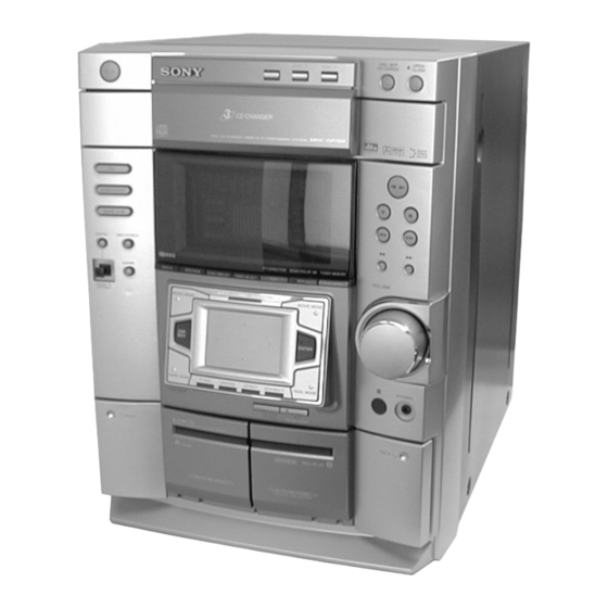
HCD-DP700 SECTION 1 GENERAL wk wl e; ea es ed Location of Parts and Controls 1 @/1 (POWER) button wh CD button 2 DISC 1-3 button wj DISPLAY 3 DISC SKIP EX-CHANGE button wk SPECTRUM button (US and AEP model only) or... - Page 5 HCD-DP700 This section is extracted from instruction manual. Turn on the system. Press CLOCK/TIMER SET on the remote. When you set the time for the first time, proceed to step 5. Press cursor V/v repeatedly to select CLOCK SET. Press ENTER.
-
Page 6: Disassemby
HCD-DP700 SECTION 2 DISASSEMBLY • The equipment can be removed using the following procedure. Case (Top) Loading Panel Front Panel Section Tape Mechanism Deck Head (A) Board, Head (B) Board And LEAF SW Board CD PANEL Board, Panel Board, OPT IN Board... - Page 7 HCD-DP700 2-2. LOADING PANEL 4 Pull-out the disc tray. CD mechanism deck (CDM58) 1 Turn the pulley to the direction of arrow. Front panel side pulley 2 Pull-out the disc tray. 2-3. FRONT PANEL SECTION qa CD mechanism deck (CDM58) 0 two screws (+BVTP 3 ×...
- Page 8 HCD-DP700 2-4. TAPE MECHANISM DECK 1 five screws (+BVTP 2.6 × 8) 2 Tape mechanism deck 2-5. CD PANEL BOARD, PANEL BOARD AND OPT BOARD 1 five screws (+BVTP 2.6 × 8) two claws qg flat type wire (CN108) 2 CD panel board...
- Page 9 HCD-DP700 2-6. ESCUTCHEON PAD (WITH TOUCH PAD) 1 button (edit) 6 two screws (TPG +P 2 × 8) 8 three screws 3 two screws (+BVTP 2.6 × 8) (+BVTP 2.6 × 8) 9 button (DSP) 2 two screws (+BVTP 2.6 × 8) 5 two screws (TPG +P 2 ×...
- Page 10 HCD-DP700 2-8. MAIN BOARD,TRANS BOARD 8 two screws 4 two screws 6 TRANS board (+BVTP 3 × 8) (+BVTT 4 × 8) 5 two screws 7 two screws (+BVTT 4 × 8) (+BVTT 3 × 8) 1 connector (CN914) 0 t wo screws (+BVTP 3 ×...
- Page 11 HCD-DP700 2-10. HEAD (A) BOARD, HEAD (B) BOARD AND LEAF SW BOARD 1 five claws 2 LEAF SW board 3 Remove the four solderings. 5 HEAD (A) board 6 HEAD (B) board 4 screw (+PTT 2 × 4), ground point 4 screw (+PTT 2 ×...
- Page 12 HCD-DP700 2-12. DRIVER BOARD, MOTOR BOARD AND CD SENSOR BOARD 8 screw (+PTPWH 2.6 × 8) 3 two screws (+BVTP 2.6 × 8) 5 MOTOR board 6 flat type wire (CN721) 4 Remove the two solderings of motor. 0 screw (+BVTP 2.6 × 8)
-
Page 13: Test Mode
HCD-DP700 SECTION 3 TEST MODE [Cold Reset] 9. To exit from this mode, press three buttons in the same manner • The cold reset clears all data including preset data stored in the as step 1, or disconnect the power cord. - Page 14 HCD-DP700 6. When the check is complete, a message of either OK or NG [Tape Deck Section] appears. • The sequence during the aging mode is following as below. • If an error occurred, stop display that step. * To return to normal mode again.
- Page 15 HCD-DP700 [CD Section] 2. CDM Error History <CDM58 Error History Display> • The sequence during the aging mode is following as below. 11 digits are displayed after the M character. Aging mode sequence (CD section): Example of display : M0FF400220000...
- Page 16 HCD-DP700 [CD Service Mode] • This mode can run the CD sled motor freely. Use this mode, for instance, when cleaning the pickup. Procedure: 1. Press POWER button to turn the set ON. 2. Select the function “CD”. 3. Press three buttons ENTER , DISC 1 , and STOP simultaneously.
-
Page 17: Mechanical Adjustments
HCD-DP700 SECTION 4 SECTION 5 MECHANICAL ADJUSTMENTS ELECTRICAL ADJUSTMENTS Precaution DECK SECTION 0 dB=0.775 V 1. Clean the following parts with a denatured alcohol-moistened swab: 1. Demagnetize the record/playback head with a head record/playback heads pinch rollers demagnetizer. erase head rubber belts 2. - Page 18 HCD-DP700 2. Turn the adjustment screw and check output peaks. If the peaks DECK B Tape Speed Adjustment do not match for L-CH and R-CH, turn the adjustment screw Note: Start the Tape Speed adjustment as below after setting to the test so that outputs match within 1dB of peak.
- Page 19 HCD-DP700 DECK B REC Bias Adjustment 4. Mode: Record Procedure: INTRODUCTION MD/VIDEO (AUDIO) IN When set to the test mode performed in Tape Speed Adjustment, 315 Hz, 50 mV (–23.8 dB) AF OSC when the tape is rewound after recording, the “REC memory mode”...
- Page 20 HCD-DP700 FM Tuned Level Adjustment CD SECTION FM RF SSG Note : 1. CD Block is basically designed to operate without adjustment. 75 Ω coaxial Therefore, check each item in order given. 2. Use LUV-P01 (4-999-032-01) unless otherwise indicated. 3. Use an oscilloscope with more than 10MΩ impedance.
- Page 21 HCD-DP700 Note: Clear RF signal waveform means that the shape “◊” can be Checking Location: clearly distinguished at the center of the waveform. [BD BOARD] RF signal waveform RF signal waveform VOLT/DIV : 200mV TIME/DIV : 500ns level : 1.45 ± 0.3Vp-p...
-
Page 22: Diagrams
HCD-DP700 SECTION 6 DIAGRAMS THIS NOTE IS COMMON FOR PRINTED WIRING BOARDS AND SCHEMATIC DIA- GRAMS. (In addition to this, the necessary note is printed in each block.) Note on Schematic Diagram: Note on Printed Wiring Boards: • X : parts extracted from the component side. -
Page 23: Circuit Board Location
HCD-DP700 6-1. CIRCUIT BOARD LOCATION • WAVEFORMS – BD BOARD – – MAIN BOARD – MOTOR board DRIVER board IC101 yj (XTAO) IC101 ra (TE) IC401 qa (XC-OUT) T301 4 CD PLAY MODE CD PLAY MODE STOP MODE TAPE B REC MODE... -
Page 24: Block Diagrams
HCD-DP700 6-2. BLOCK DIAGRAMS – TUNER/CD SECTION – FE1(E51,MX) (AEP) (EXCEPT AEP) AM/FM IF MPX FE3(AEP) LPF11 • RCH is omitted IC11 • Signal Path RF IF L-CH BUFFER IF OUT L OUT ANT IN FM IF : FM FM 75Ω... -
Page 25: Main Section
HCD-DP700 – MAIN SECTION – J601 L REC OUT IC607(1/2) SOUND PROCESSOR IC1201 MD VIDEO E51,MX L IN1 J1202 IC801 MAC IN RV1201 POWER MICVOL L IN4 TUNER L-CH LIN2 SECTION GAME J101 L-CH J602 MD/VIDEO AEP,UC,CND (AUDIO) SWOUT IC801... - Page 26 HCD-DP700 6-3. SCHEMATIC DIAGRAM – BD SECTION – • See page 23 for Waveforms. • See page 58, 59 for IC Block Diagrams. • See page 51, 52 for IC Pin Function. (Page 29)
- Page 27 HCD-DP700 6-4. PRINTED WIRING BOARD – BD SECTION – • See page 23 for Circuit Boards Location. • Semiconductor Location Ref. No. Location D101 IC101 IC102 IC103 Q101 Q102 (Page 28)
- Page 28 HCD-DP700 6-5. PRINTED WIRING BOARD – MAIN SECTION – • See page 23 for Circuit Boards Location. (Page 32) (Page 47) (Page 27) (Page 32) • Semiconductor Location Ref. No. Location A-11 D-11 D111 H-11 D112 G-12 D113 H-12 D501...
- Page 29 HCD-DP700 6-6. SCHEMATIC DIAGRAM – MAIN (1/3) SECTION – • See page 23 for Waveforms. • See page 59 for IC Block Diagrams. (Page 31) (Page 26) (Page 48) (Page 30) IC B/D (Page 30) (Page 46)
- Page 30 HCD-DP700 6-7. SCHEMATIC DIAGRAM – MAIN (2/3) SECTION – • See page 23 for Waveforms. • See page 53, 54 for IC Pin Function. (Page 34) (Page 33) (Page 29) (Page 50) AEP/US/CND MODEL : (Page 37) E51/MX MODEL :...
- Page 31 HCD-DP700 6-8. SCHEMATIC DIAGRAM – MAIN (3/3) SECTION – • See page 59, 60 for IC Block Diagrams. IC B/D IC B/D IC B/D (Page 29)
- Page 32 HCD-DP700 6-9. PRINTED WIRING BOARD – DSP SECTION – • See page 23 for Circuit Boards Location. • Semiconductor Location Ref. No. Location D607 D608 D609 D610 IC601 IC603 IC604 IC605 IC607 IC608 (Page 35) (Page 35) • Semiconductor Location Ref.
- Page 33 HCD-DP700 6-10. SCHEMATIC DIAGRAM – DSP (1/2) SECTION – • See page 61 for IC Block Diagrams. – • See page 56, 57 for IC Pin Function. (Page 30) (Page 35) TO OPT IN BOARD (Page 34) IC B/D (Page 34)
- Page 34 HCD-DP700 6-11. SCHEMATIC DIAGRAM – DSP (2/2) SECTION – • See page 61 for IC Block Diagrams. – (Page 30) (Page 33) (Page 33) IC B/D (Page 33) (Page 35)
-
Page 35: Printed Wiring Board
HCD-DP700 6-12. PRINTED WIRING BOARD – OPT SECTION – • See page 23 for Circuit Boards Location. 6-13. SCHEMATIC DIAGRAM – OPT SECTION – • See page 59 for IC Block Diagrams. (Page 32) (1/2) (Page 33) (Page 32) (2/2) -
Page 36: Printed Wiring Board Front Amp Section
HCD-DP700 6-14. PRINTED WIRING BOARD – FRONT AMP SECTION – (AEP/US/CND model) • See page 23 for Circuit Boards Location. (Page 28) (Page 28) • Semiconductor Location Ref. No. Location D801 D821 (Page 49) D830 D831 D851 D871 D881 D891... -
Page 37: Schematic Diagram Front Amp Section
HCD-DP700 6-15. SCHEMATIC DIAGRAM – FRONT AMP SECTION – (AEP/US/CND model) (Page 50) (Page 30) (Page 30) -
Page 38: Printed Wiring Board Front Amp Section
HCD-DP700 6-16. PRINTED WIRING BOARD – FRONT AMP SECTION – (E51/MX model) • See page 23 for Circuit Boards Location. (Page 28) (Page 41) (Page 28) • Semiconductor Location Ref. No. Location (Page 49) D801 D802 D821 D830 D831 D851... -
Page 39: Schematic Diagram Front Amp Section
HCD-DP700 6-17. SCHEMATIC DIAGRAM – FRONT AMP SECTION – (E51/MX model) (Page 50) (Page 30) (Page 30) (Page 40) -
Page 40: Schematic Diagram Surround Amp Section
HCD-DP700 6-18. SCHEMATIC DIAGRAM – SURROUND AMP SECTION – (Page 39) (Page 50) (Page 30) - Page 41 HCD-DP700 6-19. PRINTED WIRING BOARD – SURROUND AMP SECTION – • See page 23 for Circuit Boards Location. (Page 38) (Page 28) (Page 49) • Semiconductor Location Ref. No. Location D932 D1071 IC931 IC932 IC934 Q931 Q932...
- Page 42 HCD-DP700 6-20. PRINTED WIRING BOARD – PANEL SECTION – • See page 23 for Circuit Boards Location. • Semiconductor Location Ref. No. Location D1114 D1115 D1116 D1117 Q1114 Q1115 Q1116 • Semiconductor Location Ref. No. Location D1101 D-10 D1102 C-11...
- Page 43 HCD-DP700 6-21. SCHEMATIC DIAGRAM – PANEL (1/2) SECTION – • See page 23 for Waveforms. • See page 55 for IC Pin Function. (Page 30) (Page 44) (Page 44)
- Page 44 HCD-DP700 6-22. SCHEMATIC DIAGRAM – PANEL (2/2) SECTION – (Page 43) (Page 43)
- Page 45 HCD-DP700 6-23. PRINTED WIRING BOARD – LEAF SW SECTION – • See page 23 for Circuit Boards Location. (Page 28) • Semiconductor Location Ref. No. Location D1001 D1002 (Page 28) (Page 28) IC1001 IC1002 Q1001...
- Page 46 HCD-DP700 6-24. SCHEMATIC DIAGRAM – LEAF SW SECTION (Page 29)
- Page 47 HCD-DP700 6-25. PRINTED WIRING BOARD – DRIVER SECTION – • See page 23 for Circuit Boards Location. • Semiconductor Location Ref. No. Location D701 IC701 IC711 (Page 28)
-
Page 48: Ic Block Diagrams
HCD-DP700 6-26. SCHEMATIC DIAGRAM – DRIVER SECTION – • See page 61 for IC Block Diagrams. (Page 29) - Page 49 HCD-DP700 6-27. PRINTED WIRING BOARD – TRANS SECTION – • See page 23 for Circuit Boards Location. AEP/US/CND MODEL : (Page 36) E51/MX MODEL : (Page 38) (Page 28) • Semiconductor Location Ref. No. Location D911 D912 D913 (Page 41) Q971 •...
- Page 50 HCD-DP700 6-28. SCHEMATIC DIAGRAM – TRANS SECTION – (Page 40) (Page 30) AEP/US/CND MODEL : (Page 37) E51/MX MODEL : (Page 39)
-
Page 51: Ic Pin Functions
HCD-DP700 6-29. IC PIN FUNCTIONS • IC101 DIGITAL SIGNAL PROCESSOR (CXD3017Q) (BD Board) Pin No. Pin Name Function SOSQ Sub-Q serial output. SQCK Clock input for SQSO read-out XRST System reset. SYSM Muting input. DATA Serial date input,supplied from CPU. - Page 52 HCD-DP700 Pin No. Pin Name Function CLTV Control voltage input for master VCO. FILO Filter output for master PLL. FILI Filter input for master PLL. Chage-pump output for master PLL. AVDD3 — Analog powr supply. — Ground. — Power supply.
- Page 53 HCD-DP700 • IC401 MASTER CONTROL (M30622MGA-A36FP) (MAIN Board (2/3)) Pin No. Pin Name Function AMP-DATA Amp data signal output AMP-CLK Amp clock signal output AMP-LAT Amp latch signal output SIRCS Remote commander signal input DIG-Tx Digital common Tx signal output...
- Page 54 HCD-DP700 Pin No. Pin Name Function NO-USE Not used B TRG B deck trigger control signal output AMS-IN AMS signal input CAPM-H/L Capstan moter highi/low speed control signal output CAPM-CNT 1 Capstan moter REV/FWD/STOP control signal output A PLAY A deck play detect signal input...
- Page 55 HCD-DP700 • IC1101 DISPLAY CONTROL (MB90M407APF-G-105-BND) (PANEL Board (1/2)) Pin No. Pin Name Function 1 - 7 G7 - G1 Grid drive signal output to the fluorescent indicator 8 - 10 A1 - A3 Segment drive signal output the flourescent indicator tube Vss IO —...
- Page 56 HCD-DP700 • IC601 DECODER (CXD9617R) (DSP Board (1/2)) Pin No. Pin Name Function — Ground XRST Reset signal input EXTIN Sampling frequency switching signal input VDDI — Power supply Sampling frequency switching signal input PLOCK Internal PLL lock signal output —...
- Page 57 HCD-DP700 Pin No. Pin Name Function MOD0 Operation mode signal input (L : single chip mode, H : use prohibited) EXLOCK Lock signal input VDDI — Power supply — Ground 62 - 66 A17 - A13 External memory address output (SRAM)
-
Page 58: Ic Block Diagrams
HCD-DP700 6-30. IC BLOCK DIAGRAMS IC101 CXD3017Q (BD BOARD) 59 58 57 46 45 44 Digital LRCK PCMD OP Amp Interface Digital Asymmetry Converter Analog SW Corrector XTSL TES1 Clock EMPH Generator XVDD TEST XTAI XTAO SERVO DSP GENERATOR XVSS... - Page 59 HCD-DP700 IC103 CXA2581N-T4 (BD BOARD) OFST RW/ROM RFDCI DVCC 11 RFDCO EQ IN 26 RFC 25 VFC 24 BST AC SUM ON/OFF 23 RFG VOFST 22 VCC RW/ROM VOFST RW/ROM RW/ROM 19 TE_BAL DVCC RW/ROM 18 TE APC-OFF(Hi-Z) SW 12...
- Page 60 HCD-DP700 IC51 LC72131 (MAIN BOARD (3/3)) PHASE DETECTOR CHARGE PUMP POWER REFERENCE UNLOCK DIVIDER DETECTOR RESET SWALLOW COUNTER 1/16, 1/17 4BITS 12BITS PROGRAMMABLE DRIVER UNIVERSAL DATA SHIFT REGISTER LATCH INTERFACE COUNTER 2 3 4 5 6 7 8 9 IC81...
- Page 61 HCD-DP700 IC605 AK4527 (DSP BOARD (1/2)) IC701 BA6956AN (DRIVER BOARD) 44 43 42 41 40 39 38 37 36 35 34 AUDIO MCLK DZF2 CONTROL LOGIC RIN+ SDOS SDOUT RIN– LIN– FORMAT LIN+ CONVERTER SMUTE DATT ROUT1 BICK BICK LRCK...
-
Page 62: Exploded Views
HCD-DP700 SECTION 7 EXPLODED VIEWS NOTE: • -XX, -X mean standardized parts, so they may • Hardware (# mark) list and accessories and The components identified by have some differences from the original one. packing materials are given in the last of this mark 0 or dotted line with mark •... -
Page 63: Front Panel Section
HCD-DP700 7-2. FRONT PANEL SECTION Tape mechanism deck FL1101 not supplied Ref. No. Part No. Description Remarks Ref. No. Part No. Description Remarks 4-231-804-01 KNOB (VOL) 4-231-837-01 SPRING (TC-A) 4-231-803-01 RING (VOL) 4-231-836-01 SPRING (HEART CAM-A) X-4953-340-1 LID (B) ASSY, CASSETTE... -
Page 64: Chassis Section
HCD-DP700 7-3. CHASSIS SECTION not supplied not supplied not supplied 111 (E51) 110 (US,CND) T911 not supplied 110 (AEP, E51, MX) not supplied Ref. No. Part No. Description Remarks Ref. No. Part No. Description Remarks A-4475-627-A MAIN BOARD, COMPLETE (US, CND) -
Page 65: Tape Mechanism Deck Section-1 (Tcm-230Mwr41)
HCD-DP700 7-4. TAPE MECHANISM DECK SECTION-1 (TCM-230MWR41) • The thing that a part A curves is TCM-230MWR41. Note: Two different types of tape mechanism are used depending on models. They maintain compatibility as an entire mechanism even though there are some different parts are used. -
Page 66: Tape Mechanism Deck Section-2 (Tcm-230Awr41)
HCD-DP700 7-5. TAPE MECHANISM DECK SECTION-2 (TCM-230AWR41) • The thing that a part A doesn’t curve is TCM-230AWR41. Note: Two different types of tape mechanism are used depending on models. They maintain compatibility as an entire mechanism even though there are some different parts are used. -
Page 67: Cd Mechanism Deck Section (Cdm58E-30Bd60)
HCD-DP700 7-6. CD MECHANISM DECK SECTION (CDM58E-30BD60) M721 not supplied BU-30BD60 Ref. No. Part No. Description Remarks Ref. No. Part No. Description Remarks 4-933-134-11 SCREW (+PTPWH M2.6X8) X-4953-306-1 HOLDER (BU) (BU-30) ASSY 4-221-679-01 CAM (RELAY) X-4953-307-1 PULLEY (A) ASSY, CHUCKING 4-231-452-01 TABLE (NEW) 4-227-899-01 SCREW (DIA. -
Page 68: Base Unit Section (Bu-30Bd60)
HCD-DP700 7-7. BASE UNIT SECTION (BU-30BD60) not supplied not supplied not supplied Les composants identifiés par The components identified by mark 0 or dotted line with une marque 0 sont critiques mark 0 are critical for safety. pour la sécurité. -
Page 69: Electrical Parts List
HCD-DP700 SECTION 8 ELECTRICAL PARTS LIST NOTE: • Due to standardization, replacements in the • RESISTORS Ref. No. Part No. Description Remarks Ref. No. Part No. Description Remarks The components identified by parts list may be different from the parts All resistors are in ohms. - Page 70 HCD-DP700 CD-PANEL DRIVER Ref. No. Part No. Description Remarks Ref. No. Part No. Description Remarks R103 1-216-835-11 METAL CHIP 1/16W < TRANSISTOR > R104 1-216-839-11 METAL CHIP 1/16W R105 1-216-821-11 METAL CHIP 1/16W Q1114 8-729-900-80 TRANSISTOR DTC114ES Q1115 8-729-900-80 TRANSISTOR...
- Page 71 HCD-DP700 Ref. No. Part No. Description Remarks Ref. No. Part No. Description Remarks C604 1-164-156-11 CERAMIC CHIP 0.1uF C678 1-126-964-11 ELECT 10uF C605 1-164-156-11 CERAMIC CHIP 0.1uF C679 1-164-156-11 CERAMIC CHIP 0.1uF C680 1-126-964-11 ELECT 10uF C606 1-164-156-11 CERAMIC CHIP 0.1uF...
- Page 72 HCD-DP700 Ref. No. Part No. Description Remarks Ref. No. Part No. Description Remarks CN602 1-779-289-11 CONNECTOR, FFC (LIF(NON-ZIF)) 21P Q612 8-729-113-69 TRANSISTOR FN1F4M-M32 CN603 1-779-291-11 CONNECTOR, FFC (LIF(NON-ZIF)) 23P Q613 8-729-113-13 TRANSISTOR FA1A4M-L33 < DIODE > < RESISTOR > D601 8-719-158-02 DIODE RD3.9SB2...
- Page 73 HCD-DP700 FRONT AMP Ref. No. Part No. Description Remarks Ref. No. Part No. Description Remarks R676 1-216-809-11 METAL CHIP 1/16W R760 1-216-821-11 METAL CHIP 1/16W R677 1-216-830-11 METAL CHIP 5.6K 1/16W R761 1-216-821-11 METAL CHIP 1/16W R678 1-216-833-11 METAL CHIP...
- Page 74 HCD-DP700 FRONT AMP Ref. No. Part No. Description Remarks Ref. No. Part No. Description Remarks C808 1-128-552-51 ELECT 47uF < CONNECTOR > (US,CND,AEP) C808 1-128-560-11 ELECT 22uF 100V CN801 1-573-829-11 CONNECTOR, BOARD TO BOARD 15P (MX,E51) (AEP,US,CND) C812 1-136-165-00 FILM 0.1uF...
- Page 75 HCD-DP700 FRONT AMP HEAD (A) HEAD (B) LEAF SW Ref. No. Part No. Description Remarks Ref. No. Part No. Description Remarks R804 1-249-438-11 CARBON 1/4W R882 1-260-076-11 CARBON 1/2W 0 R805 1-220-755-11 METAL 0.22 (AEP,MX,E51) 0 R806 1-220-755-11 METAL 0.22...
- Page 76 HCD-DP700 LEAF SW MAIN Ref. No. Part No. Description Remarks Ref. No. Part No. Description Remarks < TRANSISTOR > 1-164-245-11 CERAMIC CHIP 0.015uF (MX,E51) Q1001 8-729-029-56 TRANSISTOR DTA144ESA 1-164-227-11 CERAMIC CHIP 0.022uF (US,CND,AEP) < RESISTOR > 1-164-245-11 CERAMIC CHIP 0.015uF...
- Page 77 HCD-DP700 MAIN Ref. No. Part No. Description Remarks Ref. No. Part No. Description Remarks 1-162-974-11 CERAMIC CHIP 0.01uF C331 1-126-965-91 ELECT 22uF (AEP) C332 1-137-427-11 MYLAR 120PF 1-162-924-11 CERAMIC CHIP 56PF C333 1-162-961-11 CERAMIC CHIP 330PF (AEP) C334 1-162-920-11 CERAMIC CHIP...
- Page 78 HCD-DP700 MAIN Ref. No. Part No. Description Remarks Ref. No. Part No. Description Remarks C499 1-164-156-11 CERAMIC CHIP 0.1uF D508 8-719-988-61 DIODE 1SS355TE-17 C501 1-126-964-11 ELECT 10uF D509 8-719-988-61 DIODE 1SS355TE-17 C502 1-136-165-00 FILM 0.1uF D510 8-719-988-61 DIODE 1SS355TE-17 C503 1-136-165-00 FILM 0.1uF...
- Page 79 HCD-DP700 MAIN Ref. No. Part No. Description Remarks Ref. No. Part No. Description Remarks JR19 1-216-864-11 METAL CHIP 1/16W Q304 8-729-900-63 TRANSISTOR BN1F4M-TP (US,CND,MX,E51) Q305 8-729-900-80 TRANSISTOR BA1A4M-TP JR21 1-216-864-11 METAL CHIP 1/16W Q391 8-729-140-04 TRANSISTOR 2SB1116-TP-LK JR22 1-216-864-11 METAL CHIP...
- Page 80 HCD-DP700 MAIN Ref. No. Part No. Description Remarks Ref. No. Part No. Description Remarks 1-216-809-11 METAL CHIP 1/16W R334 1-218-332-11 RES-CHIP 130K 1/16W 1-216-829-11 METAL CHIP 4.7K 1/16W R335 1-216-813-11 METAL CHIP 1/16W R336 1-216-846-11 METAL CHIP 120K 1/16W 1-216-829-11 METAL CHIP 4.7K...
- Page 81 HCD-DP700 MAIN Ref. No. Part No. Description Remarks Ref. No. Part No. Description Remarks R396 1-216-829-11 METAL CHIP 4.7K 1/16W R484 1-216-809-11 METAL CHIP 1/16W R397 1-216-820-11 METAL CHIP 1/16W R486 1-216-809-11 METAL CHIP 1/16W R398 1-216-823-11 METAL CHIP 1.5K...
- Page 82 HCD-DP700 MAIN MOTOR OPT IN OPT IN REAR PANEL Ref. No. Part No. Description Remarks Ref. No. Part No. Description Remarks < VIBRATOR > A-4726-481-A PANEL BOARD, COMPLETE (CND) *************************** 1-760-549-31 VIBRATOR, CRYSTAL (4.5MHz) 1-579-900-21 VIBRATOR, CRYSTAL (4.332MHz)(AEP) 4-224-584-01 HOLDER (FL) (CND,AEP,MX,E51) X401 1-567-098-41 VIBRATOR, CRYSTAL (32.768kHz)
- Page 83 HCD-DP700 PANEL Ref. No. Part No. Description Remarks Ref. No. Part No. Description Remarks C1212 1-124-584-00 ELECT 100uF Q1111 8-729-900-80 TRANSISTOR DTC114ES (MX,E51) Q1112 8-729-900-80 TRANSISTOR DTC114ES C1213 1-126-157-11 ELECT 10uF Q1113 8-729-119-78 TRANSISTOR 2SC2785-HFE (MX,E51) Q1120 8-729-119-78 TRANSISTOR 2SC2785-HFE...
- Page 84 HCD-DP700 PANEL Ref. No. Part No. Description Remarks Ref. No. Part No. Description Remarks R1160 1-249-419-11 CARBON 1.5K 1/4W F R1285 1-249-417-11 CARBON 1/4W F R1161 1-249-421-11 CARBON 2.2K 1/4W F R1162 1-249-422-11 CARBON 2.7K 1/4W F R1286 1-249-417-11 CARBON...
- Page 85 HCD-DP700 CD SENSOR SUB TRANS SURROUND AMP Ref. No. Part No. Description Remarks Ref. No. Part No. Description Remarks 1-675-911-14 CD SENSOR BOARD < TRANSISTOR > **************** Q901 8-729-119-78 TRANSISTOR 2SC2785-HFE < CAPACITOR > < RESISTOR > C712 1-164-159-11 CERAMIC 0.1uF...
- Page 86 HCD-DP700 TRANS Ref. No. Part No. Description Remarks Ref. No. Part No. Description Remarks R1072 1-249-441-11 CARBON 100K 1/4W (MX,E51) MISCELLANEOUS ************************************************************** *************** 0 M961 1-680-189-11 TRANS BOARD 1-763-072-11 FAN. DC 1-796-001-11 TOUCH PAD ************* FL1101 1-518-722-11 INDICATOR TUBE, FLUORESCENT <...
- Page 87 HCD-DP700 Ref. No. Part No. Description Remarks Ref. No. Part No. Description Remarks 4-231-990-61 INSTRUCTION MANUAL (DUTCH, ITALIAN, POLISH) (AEP) ************************************************************ ************** HARDWARE LIST ************** 7-685-646-79 SCREW +BVTP 3X8 TYPE2 N-S 7-685-647-79 SCREW +BVTP 3X10 TYPE2 N-S 7-685-105-19 TPG +P 2X8, TYPE2 N-S...
- Page 88 HCD-DP700 REVISION HISTORY Clicking the version allows you to jump to the revised page. Also, clicking the version at the upper right on the revised page allows you to jump to the next revised page. Ver. Date Description of Revision...
Need help?
Do you have a question about the HCD-DP700 and is the answer not in the manual?
Questions and answers