Table of Contents
Advertisement
Important Service Notes ............................................................................................................................................ 2
Specifications ................................................................................................................................................................. 2
NAMES OF PARTS ............................................................................................................................................................... 3
Operation Manual .......................................................................................................................................................... 4
Quick Guide ....................................................................................................................................................................... 7
Disassembly ...................................................................................................................................................................... 8
Removing And Reinstalling The Main Parts ....................................................................................................... 11
Adjustment ..................................................................................................................................................................... 14
Explanation Of Error Display ................................................................................................................................ 29
Explanation Of Mechanism Error ......................................................................................................................... 30
Notes On Schematic Diagram .................................................................................................................................. 33
Block Diagram ............................................................................................................................................................... 34
Schematic Diagram/Wiring Side Of P.w.board ................................................................................................... 40
Voltage (Md Main Pwb) ................................................................................................................................................ 58
Waveforms Of Cd Circuit .......................................................................................................................................... 59
Waveforms Of Md Circuit .......................................................................................................................................... 60
TROUBLE SHOOTING ........................................................................................................................................................ 62
Function Table Of Ic .................................................................................................................................................... 71
Parts Guide/EXPLODED VIEW
SERVICE MANUAL
CONTENTS
SHARP CORPORATION
– 1 –
• In the interests of user-safety the set should be restored to its
original condition and only parts identical to those specified should
be used.
This document has been published to be used
for after sales service only.
The contents are subject to change without notice.
MD-R3
No. S2814MDR3////
MD-R3
Page
Advertisement
Table of Contents
Troubleshooting

Subscribe to Our Youtube Channel
Related Manuals for Sharp MD-R3


Summary of Contents for Sharp MD-R3
- Page 1 MD-R3 SERVICE MANUAL No. S2814MDR3//// MD-R3 • In the interests of user-safety the set should be restored to its original condition and only parts identical to those specified should be used. CONTENTS Page IMPORTANT SERVICE NOTES ............................2 SPECIFICATIONS ................................. 2 NAMES OF PARTS ................................
-
Page 2: Important Service Notes
MD-R3 FOR A COMPLETE DESCRIPTION OF THE OPERATION OF THIS UNIT, PLEASE REFER TO THE OPERATION MANUAL. IMPORTANT SERVICE NOTES BEFORE RETURNING THE AUDIO PRODUCT (Fire & Shock Hazard) Before returning the audio product to the user, perform the following safety checks. -
Page 3: Names Of Parts
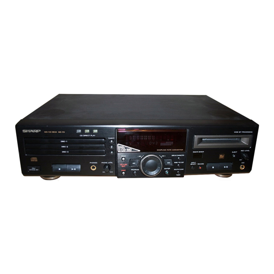
MD-R3 NAME OF PARTS Front panel DISC TRACK DATE OVER 1 2 3 4 5 6 7 TOTAL 8 9 10 11 12 13 REMAIN 15 16 17 18 19 20 MONO LP PRGM RANDOM TIMER REC CLOCK 14 1516... -
Page 4: Operation Manual
MD-R3 Names of controls 1. Direct Key Buttons 2. Play Mode Button 3. Music Scan Button 4. Input Select Button 5. Display Button 6. Auto Mark Button 7. Time Button 8. MD Track Up/Cue Button: 9. MD Track Down/Review Button: 10. - Page 5 MD-R3 – 5 –...
- Page 6 MD-R3 – 6 –...
- Page 7 MD-R3 – 7 –...
-
Page 8: Disassembly
MD-R3 DISASSEMBLY Top Cabinet (A1)x1 Caution on Disassembly ø3x10mm Follow the below-mentioned notes when disassembling the unit and reassembling it, to keep it safe and ensure excellent performance: 1. Take the minidisc out of the unit. 2. When disassembling the machine, be sure to withdraw the power plug from the socket in advance. - Page 9 MD-R3 Shield Case CD Changer Servo PWB Block (R1) x 2 ø3 x 6mm Tray Switch (M2)x3 (R1) x 2 (M1)x3 (N2)x2 ø3 x 6mm ø3x10mm MD Mechanism Unit (P1)x1 ø2x7mm CD Changer PWB (N1)x2 (Remove 4 soldering joints). ø2.6x10mm...
- Page 10 MD-R3 • Jog knob replacement procedure Jog Knob Jog Decoration FL Window Jog Decoration Front Panel VOLUME Display PWB Jog Knob Push directly the jog knob with pliers etc. Figure 10-1 Display PWB Remove the pawl of jog decoration with fine piece such as tweezers, press, and remove the jog knob.
-
Page 11: Removing And Reinstalling The Main Parts
MD-R3 REMOVING AND REINSTALLING THE MAIN PARTS (A1) x2 CD MECHANISM SECTION ø2.6 x5mm Stop Washer For the procedure to remove the CD mechanism from the (A3) x1 main unit, refer to Disassembling Procedure, Steps 1, 5, 11, Pickup and 14. - Page 12 MD-R3 (A1)x1 MD MECHANISM SECTION ø1.7x5mm Perform steps 1, 3, 15 to 17 of the disassembly method to remove the MD mechanism. Magnetic Head How to remove the magnetic head (See Fig. 12-1) 1. Remove the screws (A1) x 1 pc.
- Page 13 MD-R3 How to remove the sled motor/loading motor (See Fig. 13-1) (D1)x2 (D1)x2 Ø1.7x2mm Ø1.7x2mm 1. Remove the screws (D1) x 1 pcs., and remove the sled motor/loading motor. Caution: Be careful so that the gear is not damaged. (The damaged gear emits noise during searching.)
-
Page 14: Adjustment
MD-R3 ADJUSTMENT CD SECTION Extension cable When making adjustment or checking operation, use the following extension cable as necessary. Type Extension cable Parts No. For CD PWB (TP751, 6-pin) QCNWK0043AFZZ CD SERVO PWB CNP700A TP751 BI851/CNS552 CNP751 CNS903 Extension cable for... - Page 15 MD-R3 Button operation in CD test mode 1. [STOP] : Specific operation is stopped, resulting in TEST mode waiting state. The pickup slide is kept in stop state. 2. [ : The pickup slides toward the external periphery. 3. [ : The pickup slides toward the internal periphery.
- Page 16 MD-R3 Reference Vertically CD level symmetrical 1/2 VCC waveform 0.5~1.5Vp - p Adjust to get uniform and minimized error waveform. Figure 16-1 TRACKING ERROR BALANCE Apply a black tape Figure 16-3 FOCUS OFFSET/TRACKING OFFSET (1.2 to 1.5 wide). Waveform TP751, pin 1...
-
Page 17: Test Mode
MD-R3 TEST MODE 1) Mode there are 5 kinds TEST MODE as below. MODE PUSH KEY A) MD TEST MODE ENTER PLAY B) AUDIO TEST MODE REVIEW C) KEY TEST MODE ENTER 2) How to start and quit TEST MODE. - Page 18 MD-R3 KEY TEST KEY NAME ILLUMINATE KEY NAME ILLUMINATE SEGMENT SEGMENT TIMER 10 ROW DOT INPUT SELECT DISPLAY 11 ROW DOT EJECT 7 ROW DOT REVIEW PLAY 4 ROW DOT STOP 5 ROW DOT ENTER 8 ROW DOT 6 ROW DOT JOG.
- Page 19 MD-R3 • Test Mode 1. EJECT mode • TEMP setting (of EEPROM setting) • CONTROL setting (of EEPROM setting) • Setting of laser power (record/playback power) 2. AUTO pre-adjustment mode • Automatic pre-adjustment is performed. (After adjustment the grating adjustment mode is set.) •...
- Page 20 MD-R3 2. AUTO pre-adjustment mode (Low reflection disc only) Setting Method Step No. Remarks Display Step 1 Testmode STOP state [ t s m Step 2 Press once the ENTER button. AUTO pre-adjustment menu A U T O Step 3 Press once the MD PLAY button.
- Page 21 MD-R3 Step No. Setting Method Remarks Display Step 18 Press once the ENTER button. Indication of measurement value [ L B O : _ _ _] Step 19 Press once the ENTER button. Indication of measurement value [ L E O :...
- Page 22 MD-R3 Step No. Setting Method Remarks Display Step 22 Press once the ENTER button. Focus ATT (B signal) setting [ S B G : Step 23 Press once the ENTER button. Offset "0" setting A signal offset measurement [ H A O :...
- Page 23 MD-R3 8. EEPROM setting mode a) Focus setting Step No. Setting Method Remarks Display Step 1 Testmode STOP state [ t s m Step 2 Press the ENTER button seventimes. EEPROM setting menu [E E P R O M _ S E T] Step 3 Press once the MD PLAY button.
- Page 24 MD-R3 Step No. Setting Method Remarks Display Step 11 Press once the ENTER button. Tracking kick pulse level setting (for one line jump) [ T R K L V 0 _ _ Step 12 Press once the ENTER button. Tracking kick pulse level setting (for 10 line jump)
- Page 25 MD-R3 e) TEMP setting Setting Method Step No. Remarks Display Step 1 Testmode STOP state [ t s m Step 2 Press the ENTER button seven times. EEPROM setting menu [E E P R O M _ S E T] Step 3 Press once the MD PLAY button.
- Page 26 MD-R3 g) ADJUST setting Setting Method Step No. Remarks Display Step 1 Test mode STOP state [ t s m (or continuous record/playback state or specific menu state of other mode) Step 2 Input the B2h command 7 times, including NOP...
- Page 27 MD-R3 • Whenever the DISPLAY/CHARACTER button is pressed in the continuous playback mode, the indication changes as follows. * Pit section Continuous playback (SUBQ address indication + C1 error indication) remains. * Groove section Continuous playback (ADIP address indication + C1 error indication) remains.
- Page 28 MD-R3 Mechanism Adjustment 1. Optical pickup grating inspecting method OSILLOSCOPE 42 pin of IC 1101 GND (TP1131) 100K 26 pin of IC 1101 EOUT (TP1133) 470p GND CH1 CH2 470p Spindle Motor 25 pin of IC 1101 100K FOUT (TP1132)
-
Page 29: Explanation Of Error Display
MD-R3 EXPLANATION OF ERROR DISPLAY Error display Errors Corrective action Can't REC • Defect occurred successively 10 times during REC-PLAY. • Check that the disc is free from flaw, dust • As a result of occurrence of defect during REC-PLAY the and fingerprint. -
Page 30: Explanation Of Mechanism Error
MD-R3 Error display Corrective action Errors DEFECT • Focusing error was caused by shock during REC-PLAY. • Check that the disc is free from flaw, dust, fingerprint and black spot. Check for disc disalignment and run-out. TOC W ERROR • Although UTOC can be read but UTOC cannot be rewritten. - Page 31 MD-R3 -PROM Data List Focus setting Slide setting Initial Setting Item indication Initial Setting Item indication S L G S L 2 F F 1 S L D L I M F F 2 S L D L E V...
- Page 32 MD-R3 -PROM Setting Mode Chart Figure 32 – 32 –...
-
Page 33: Notes On Schematic Diagram
MD-R3 NOTES ON SCHEMATIC DIAGRAM • The indicated voltage in each section is the one measured by • Resistor: Digital Multimeter between such a section and the chassis To differentiate the units of resistors, such symbol as K and with no signal given. -
Page 34: Block Diagram
MD-R3 CH1-OUTA D. BUF OPTICAL PICKUP UNIT – + CH1-OUTB D. BUF CH1-INA FOCUS COIL CH1-INB TRACKING COIL TR-B – + CD+5V VREG OUT VOLTAGE REGULATOR MUTE Q701 IC700 BA5914FP FOCUS/TRACKING/ SPIN/SLIDE DRIVER LASER DRIVER Q751 CH2-INB – CH2-INA CD+5V... - Page 35 MD-R3 CH1-OUTA D. BUF – + – CH1-OUTB CH4-OUTA M702 SLED D. BUF D. BUF MOTOR CH4-OUTB CH1-INA M701 SPINDLE D. BUF MOTOR CH4-INA CH1-INB TR-B CH4-INB SW702 + – – + PICKUP IN BIAS IN VREG OUT LTAGE GULATOR...
- Page 36 MD-R3 TX301 DIGITAL OUTPUT MD UNIT SYSCL 74HC10AP J301 IC302 COAXIAL IN NAND GATE IC301 INVERTER 74HCU04 RX301 DIGITAL INPUT Q930 Q935 BUTTON BLOCK JOG VOLUME SW901 CD5V CD UNIT BACK UP 5V CD7.5V FL VP IC901 SW501 RESET IX0240AW...
- Page 37 MD-R3 A–9V VR101 REC VOL 2 9 4 8 3 VINL,VINR A+9V J101 IC101 LINE IN A–9V NJU4560D IC380 LINE IN AMP MC14066B A+9V IC201 SYSCLK,WS,DATA0,DATA1 ANALOG SWITCH UDA1340 AD/DA CONVERTER L3MODE L3CLK L3DATA J351 Q380 26 24 25 23 10 MIC JACK A–9V...
- Page 38 MD-R3 Figure 38 BLOCK DIAGRAM (5/6) – 38 –...
- Page 39 MD-R3 SWITCHING QB102 TRAY MOTOR MOB2 MOB1 MAIN CAM MOTOR – – VREF VREF OUT1 OUT1 M GND M GND OUT2 OUT2 M +9V M +9V MICOM 44 43 42 41 SW-B SW-1 SW-C IKISUGI SW-D CLOCK ICB101 M-CONT1 MODE DATA...
- Page 40 MD-R3 Q751 R753 2SA1015 GR 1/2VCC C751 C750 4.7/25 – IC750 M62472FP 1/2VCC – R793 120K SERVO CONTRO R792 120K – R790 120K – – R791 I/V AMP. – 120K HF AMP. – R794 R755 – HFOK VR1A – R795...
- Page 41 MD-R3 IC750 M62472FP R760 ERVO CONTROL C774 4.7K R758 (CH) – HF– – I/V AMP. R759 HF AMP. – C773 R781 0.001 HFOK 1.2K CD SIGNAL – – C772 C811 7.7K CNS502 0.033 100/10 P47 8 - H 330K CD 5V FE AMP.
- Page 42 MD-R3 RB161 ICB104 220K RESET M.GND 5.08V 4.9V M+9V CB141 CB140 0.1 (ML) 0.1 (ML) XB101 3MHz LB103 100 H RB103 P47 9 - H D.GND 11 10 CNP505 M.GND LB102 D.GND TO MAIN PWB 10 H LB105 10 H...
- Page 43 MD-R3 ICB102 TA7291S LOADING MOTOR DRIVER 5.07V CB125 100P RB139 5.06V RB141 1 (1/2W) 0.8V CB121 100/16 0.8V RB140 SW-A 5.07V KEY OUT0 RB142 5.07V KEY OUT1 CB123 0.047 KEY OUT2 (ML) 5.07V KEY OUT3 5.07V D+5V CB134 5.07V D+5V...
- Page 44 MD-R3 P46 1 - C TO MAIN PWB P46 4 - A P47 11 - B CNP351 TO MAIN PWB TO MAIN PWB CNP101 CNP652 CNS351 CNS652 CNS101 3 2 1 HEAD BI351 MIC PWB-B3 VR651-1 1K(C) HEADPHONES VOLUME C358...
- Page 45 MD-R3 HEADPHONES PWB-B2 C925 C927 0.001 0.001 FL901 J651 C926 C928 C661 0.001 0.001 0.001 HEADPHONES C662 0.001 CNS651 CNP651 C663 CNW655 C901 C902 –31V C903 R963 R945 R931 R935 100 99 98 97 96 95 94 93 92 91 90 89 88 87 86 85 84 83 82 81 H OPEN –27V...
- Page 46 MD-R3 P44 4 - A TO DISPLAY PWB CNS101 IC101-1 NJM4560D C107 R103 R109 OPE AMP. CNP101 1/50 R101 C115 47/10 L-CH C109 L-CH (1/2) C101 C103 220P R105 0.022 100P R119 C105 100K – L101 R107 220P (CH) 100K 7.8V...
- Page 47 MD-R3 )...MUTE ON Q451 C451 R451 2SC2878 B R455 47/10 MUTE L-CH –6.3V(0.6V) C455 R453 C459 820P IC601-1 470P R457 C453 470P NJM4580D LINE AMP. R607 J101 L451 R617 C613 LINE OUT 0.22 H 0.01V 47/10 )...MUTE ON C607 (1/2) –6.3V...
- Page 48 MD-R3 TP1141 TP1131 C1107 C1110 0.0047 TP1275 0.47 C1106 TP1142 0.47 99 98 97 96 95 94 EFMAGI EFMAGC C1119 ADIPI 330P TP1274 TP1140 EFMMON (CH) R1155 AVCC ADIPO EFMO-I EFMO-I C1202 TP1139 EFMI 99 98 & AGND DIFF AOUT-IN...
- Page 49 MD-R3 MD MAIN PWB-E ANALOG PLAY BACK SIGNAL DIGITAL RECORD SIGNAL DIGITAL PLAYBACK SIGNAL R1211 C1208 0.047 TP1275 TP1210 99 98 97 96 95 94 93 92 91 90 89 88 87 86 85 84 83 82 81 80 79 78 77 76...
- Page 50 MD-R3 P56 3 - A P52 5 - A TO MD MAIN PWB TO DISPLAY PWB CN1902 CNP901 FC402 FC401 P54 2 - E TO CD SERVO CNS502 IC501 R418 R417 D651 C227 C118 22201816141210 8 6 4 2 CNP402...
- Page 51 MD-R3 P54 2 - E P53 11 - A MAIN PWB-A TO CD SERVO PWB TO CD CHANGER PWB CNS502 CNS505 Q502 D554 Q501 F552 F551 D502 D553 R503 D552 C544 C504 D551 C503 5 17 19 21 23 16 18 20 22 24...
- Page 52 MD-R3 DISPLAY PWB-B1 Rec. VR101 Volume COLOR TABLE BROWN P50 5 - A RD(R) CNP402 ORANGE CNS101 TO MAIN PWB IC902 YELLOW P50 1 - C GREEN CNP101 BLUE TO MAIN PWB J351 VIOLET MIC PWB-B3 R923 C909 GRAY R906...
- Page 53 MD-R3 P50 5 - H P51 8 - B TO MAIN PWB TO MAIN PWB CNP505 CNP504 CNS504 CNS505 5 4 3 2 1 1 2 3 4 BIB101 BIB102 6 5 4 3 2 1 LB103 CB141 CB102 ICB104...
- Page 54 MD-R3 P52 6 - B TO DISPLAY PWB CD MOTOR PWB-G CNS903 CD SERVO PWB-C FOCUS R812 OFFSET TRACKING R757 GAIN R761 PICKUP IN TP751 VR753 TRACKING C756 SPIN MOTOR R763 ERROR VR752 M701 TRACKING BALANCE R762 R764 OFFSET R809...
- Page 55 MD-R3 MD SPINDLE M901 COLOR TABLE BROWN RD(R) ORANGE YELLOW GREEN BLUE TO MD MAIN PWB VIOLET CN1603 GRAY P56 1 - F WH(W) WHITE BLACK PINK MD SLED M902 MD LOADING M903 TO MD MAIN PWB CN1602 TO MD MAIN PWB...
- Page 56 MD-R3 P50 4 - A TO MAIN PWB CNP401 MD MAIN PWB - E (TOP VIEW) CN1902 CN1252 TO MAGNETIC Q1820 HEAD C1251 P55 9 - H C1252 R1251 R1827 R1459 R1939 R1463 Q1253 Q1254 C1425 R1461 R1940 R1223 IC1251...
- Page 57 MD-R3 P51 10 - H TO MAIN PWB MD MAIN PWB - E (BOTTOM VIEW) CNP301 TP1518 TP1504 TP1516 TP1519 R1947 TP1520 TP1908 TP1524 TP1502 TP1252 TP1522 TP1512 TP1503 TP1501 R1759 TP1907 R1805 TP1521 TP1523 Q1807 TP1905 R1758 COLOR TABLE...
-
Page 58: Voltage (Md Main Pwb)
MD-R3 VOLTAGE (MD MAIN PWB) IC1601 IC1916 Q1801 IC1907 IC1201 IC1401 VOLTAGE NO. VOLTAGE NO. VOLTAGE NO. VOLTAGE NO. VOLTAGE NO. VOLTAGE VOLTAGE 1.25V 1.58V 2.8V 1.48V 3.2V 2.6V 1.5V 1.58V 4.9V 1.6V 0.2V 5.5V 3.2V 2.6V 3.2V 5.5V DIC input:2.2V 1.6V... -
Page 59: Waveforms Of Cd Circuit
MD-R3 WAVEFORMS OF CD CIRCUIT 0.2V/1mS (DC range) IC700 2V/1mS (DC range) [Disc playback mode] [Disc playback mode] Potential difference 0V 1/2VCC Disc free from flaw TRIG Disc having flaw IC750 (the same as above) In test mode 2 (disc is not loaded. -
Page 60: Waveforms Of Md Circuit
MD-R3 WAVEFORMS OF MD CIRCUIT PLAY STATE PIT PLAY Stopped Stopped NORM: 100M S/s NORM: 1M S/s 1997 / 08 / 04 09:30:15 1997 / 08 / 04 13:35:24 CH1 500mV 200mV 500ns/div 1ms/div AC 10:1 DC 10:1 DC 10:1... - Page 61 MD-R3 PLAY Stopped Stopped NORM: 1k S/s NORM: 100M S/s 1997 / 08 / 04 14:19:52 1997 / 08 / 04 11:23:12 1s/div 2us/div DC 10:1 DC 10:1 DC 10:1 DC 10:1 DC 10:1 DC 10:1 DC 10:1 Filter Filter...
-
Page 62: Trouble Shooting
MD-R3 TROUBLE SHOOTING (CD SECTION) CD fails to operate If the objective lens of optical pickup is contaminated, CD may fail to operate. At first clean the objective lens, and check playback operation. If CD does not operate persistently, check as follows. - Page 63 MD-R3 • Laser does not light Is 5V applied to the pin 13 CD LD ON terminal of IC901? IC901 is defective. Is +5V applied to the C751 side of Is +4.0V applied to the emitter of Q751? R753 is defective.
- Page 64 MD-R3 • Track search failure Set the TEST mode, and check whether the slide motor is Check as stated in item "Slide motor fails to run". started with (skip) (skip). s the following waveform output to the pin 29 of IC750 in track IC750 is defective.
- Page 65 MD-R3 • Spindle motor CLV servo failure Does the spindle motor run in the CD TEST mode3? Is voltage generated for about 0.3 to Spindle motor failure 1.5 sec between the pins 17 and 18 or wire breakage. of IC700 when the mode is changed...
- Page 66 MD-R3 TROUBLE SHOOTING (MD SECTION) When MD fails operate If the objective lens of optical pickup is contaminated, MD may fail to operate. At first, clean the objective lens to check playback operation. If MD fails persistently to operate, perform checks as follows.
- Page 67 MD-R3 • Disc loading is not normal. Is disc loaded when it is inserted? Check CNP1601 and SW1956. Is the pin 4 of CNP1601 set to L state? Is change observed on the pin 23 or 24 of IC1601? Check IC1401.
- Page 68 MD-R3 • Normal playback When it has been confirmed that EEPROM value is normal in the TEST mode Is initialization performed normally when high reflection disc is Does the playback time display advance? played back? Check IC1201 Does disc rotate normally?
- Page 69 MD-R3 • Record and playback operation Insert the low reflection disc, and after verifying the audio output in the normal mode playback set the record/playback TEST mode Recording from start address cannot be performed. Check whether the disc is record-prohibited.
- Page 70 MD-R3 • Disc motor fails to run Check soldering joint and parts of pins 24 and 25 of IC1201, and Does waveform appear on the pins 24 and 25 of IC1201 in the peripheral circuit. TEST mode focus gain coarse adjustment step?
-
Page 71: Function Table Of Ic
MD-R3 FUNCTION TABLE OF IC IC901 RH-iX0240AWZZ: System Control Microcomputer (IX0240AW) (1/2) Terminal Name Input/Output Port Name Function Pin No. P77/AN7-P75/AN5 KEY1-KEY3 Input Key input P74/AN4 — Input Not used P73/AN3 Input Initial setting read-in P72/AN2 JOG_AD Input Jog dial read-in... - Page 72 MD-R3 IC901 RH-iX0240AWZZ: System Control Microcomputer (IX0240AW) (2/2) Terminal Name Input/Output Pin No. Port Name Function 65-71 P37/SEG31- S31-S25 Output Segment for FL drive P31/SEG25 P30/SEG24 Output Segment for FL drive 73-80 P97/SEG23- S0-S8 Output Segment for FL drive P90/SEG16...
- Page 73 MD-R3 IC1101 VHiiR3R55//-1:RF Signal Control (IR3R55) Function Terminal Name Pin No. RF signal input terminal 1 Input of RF signal output of pickup RF signal input terminal 2 Input of RF signal output of pickup RF signal input terminal 3 Input of RF signal output of pickup...
- Page 74 MD-R3 IC1201 VHiLR376481-1:ENDEC/ATRAC (LR376481) (1/2) Input/Output Function Terminal Name Pin No. EFMMON Output EFM monitor output AVCC — Analog power EFMI Input EFM signal input from RF amp. AGND — Analog GND Input Focus error signal A Input Tracking error signal E...
- Page 75 MD-R3 IC1201 VHiLR376481-1:ENDEC/ATRAC (LR376481) (2/2) Function Terminal Name Input/Output Pin No. TESO1 Output PLLLR. Microcomputer extension output port 2 in case of selection TESO3 In/Output PLLOSC. Microcomputer extension output port 3 in case of selection TEST4 In/Output EXTCLK. Microcomputer extension output port 4 in case of selection...
- Page 76 MD-R3 IC1401 RX-iX0232AWZZ:MD System Microcomputer (IX0232AW) (1/2) Function Terminal Name Input/Output Pin No. P96/ANEX1 Output Not used P95/ANEX0 Output Not used P94/DA1 Output LDVAR (laser power adjustment output) P93/DA0 Output ADJS (for automatic adjustment step check) P92/TB2 Output Not used...
- Page 77 MD-R3 IC1401 RX-iX0232AWZZ:MD System Microcomputer (IX0232AW) (2/2) Input/Output Function Terminal Name Pin No. P42/A18 In/Output SYS D2 (data bus 2) P41/A17 In/Output SYS D1 (data bus 1) P40/A16 In/Output SYS D0 (data bus 0) P37/A15 Output Not used P36/A14 Output...
- Page 78 MD-R3 IC1101 VHiiR3R55//-1:RF Signal Control (IR3R55) ADIPI ADIPO DIFF DIFF ADLPFO ADIP REFI 22KO REFO 22KI BIAS RFADD TCGI TCGO AOUT BOUT EOUT LOGIC FOUT Figure 78-1 BLOCK DIAGRAM OF IC IC1201 VHiLR376481-1:ENDEC/ATRAC (LR376481) 75 74 73 72 71 70 69 68 67 66 65 64 63 62 61 60 59 58 57 56 55 54 53 52 51...
- Page 79 “HOW TO ORDER REPLACEMENT PARTS” To have your order filled promptly and correctly, please furnish the For U.S.A. only following information. Contact your nearest SHARP Parts Distributor to order. 1. MODEL NUMBER 2. REF. No. 3. PART NO. 4. DESCRIPTION For location of SHARP Parts Distributor, Please call Toll-Free;...
- Page 80 MD-R3 PRICE PRICE PART CODE DESCRIPTION PARTS CODE DESCRIPTION RANK RANK INTEGRATED CIRCUITS D508 VHEMTZJ270D-1 AA Zener,27V,MTZJ27D D509,510 VHD1SS133//-1 AA Silicon,1SS133 IC101 VHINJM4560D-1 AH Ope Amp.,NJM4560D D511 VHERD9R1JS1-1 AA Zener,9.1V,RD9.1JS1 IC201 VHIUDA1340/-1 BA AD/DA Converter,UDA1340 D512 VHEMTZJ8R2C-1 AB Zener,8.2V,MTZJ8.2C IC301...
- Page 81 MD-R3 PRICE PRICE DESCRIPTION PARTS CODE DESCRIPTION PART CODE RANK RANK C224 VCKYTV1HF223Z AA 0.022 F,50V C761 VCKYTV1HB223K AA 0.022 F,50V C225,226 VCKYPU1HB101K AA 100 pF,50V C762 VCKYTV1CB104K AA 0.1 F,16V C227 VCKYTV1EF104Z AA 0.1 F,25V C763 RC-GZA106AF1C AB 10 F,16V,Electrolytic...
- Page 82 MD-R3 PRICE PRICE PART CODE DESCRIPTION PARTS CODE DESCRIPTION RANK RANK C1631 VCKYTV1CF105Z AB 1 F,16V R313 VRD-ST2CD102J AA 1 kohm,1/6W C1650~1653 VCCSCY1HL821J AA 820 pF,50V R350 VRS-TV2AB101J AA 100 ohm,1/10W C1654,1655 VCKYCY1EB153K AA 0.015 F,25V R351,352 VRS-TV2AB104J AA 100 kohm,1/10W...
- Page 83 MD-R3 PRICE PRICE DESCRIPTION PARTS CODE DESCRIPTION PART CODE RANK RANK R772 VRS-TV2AB823J AA 82 kohms,1/10W R1261~1263 VRS-CY1JB103J AA 10 kohm,1/16W R773 VRS-TV2AB562J AA 5.6 kohms,1/10W R1266 VRS-CY1JB103J AA 10 kohm,1/16W R774 VRS-TV2AB473J AA 47 kohms,1/10W R1281 VRS-CY1JB470J AA 47 ohms,1/16W...
- Page 84 MD-R3 PRICE PRICE PART CODE DESCRIPTION PARTS CODE DESCRIPTION RANK RANK R1962 VRS-CY1JB224J AA 220 kohms,1/16W CNS902 QCNWN1167AWZZ J AH Connector Ass’y,5Pin R1963 VRS-CY1JB152J AA 1.5 kohms,1/16W CNS903 QCNWN1168AWZZ J AL Connector Ass’y,12Pin R1964 VRS-CY1JB682J AA 6.8 kohms,1/16W CNS1252 QCNWN1044AWZZ J AG Connector Ass’y,2Pin...
- Page 85 MD-R3 PRICE PRICE DESCRIPTION PARTS CODE DESCRIPTION PART CODE RANK RANK MLEVP0076AWZZ J AC Lever,Catch NROLP0007AWZZ J AB Rollar,Cam Guide MLEVP0077AWZZ J AC Lever,Slider NPLYR0004AWZZ AC Pulley,Drive MSPRD0103AWFJ J AB Spring,Roller Holder NGERH0052AWZZ J AC Gear,Idler MSPRD0105AWFJ J AB Spring,Spin...
-
Page 86: Quick Guide
MD-R3 PRICE PRICE PART CODE DESCRIPTION PARTS CODE DESCRIPTION RANK RANK GCOVA1165AWSA J AL Cover,CD Tray 3 HDECP0042AWSA J AE Filter,Remote Control JKNBZ0444AWSA AH Knob,Edit JKNBZ0442AWSA AG Knob,CD Edit JKNBZ0443AWSA AH Knob,MD JKNBZ0445AWSA AH Knob,Disc Select PRDAR0102AWFW J AG Heat Sink... - Page 87 MD-R3 306-2 306-1 306-3 703x2 M701 M702 305x2 SW702 PWB-G Figure 8 CD MECHANISM EXPLODED VIEW – 87 – – 8 –...
- Page 88 MD-R3 CD Mechanism 805x4 803x2 804x3 104 105 801x2 111x2 110x2 108x3 108x3 SWB101 PWB-H ~104 108x3 MOB1 123x4 PWB-D MOB2 80mm 806x2 Figure 9 CD CHANGER MECHANISM EXPLODED VIEW – 9 – – 88 –...
- Page 89 MD-R3 611x2 CNS1252 611x2 SW1956 PWB-F SW1953 1952 SW1955 SW1954 603x2 CFW1901 603x2 PWB-E 612x4 M902 M903 M901 606x3 Figure 10 MD MECHANISM EXPLODED VIEW – 89 – – 10 –...
- Page 90 MD-R3 606x3 606x5 CD Changer Unit 609x3 PWB-B2 613x3 PWB-C PWB-B5 602x2 602x6 PWB-B4 614x3 FL901 602x11 602x2 201-1 PWB-B1 201-2 PWB-B3 MD Unit Silicon 610x4 603x2 Grease 603x2 607x2 608x2 605x4 PWB-A with SW901 226x6 222x2 221x2 606x2 609x2...
-
Page 91: Packing Of The Set
MD-R3 PACKING OF THE SET Feature Label Polyethylene Bag, Unit SSAKP0056AWZZ Polyethylene Bag, Accessories SSAKH0025AWZZ • Operation Manual • Quick Guide Remote Control Polyethylene Bag, Warranty 92LBAG667B Analog Connecting Cable x 2 Packing Add.,Left/Right SPAKA0164AWZZ Packing Case SPAKC0636AWZZ Bar Cord Label : Not Replacement Item –... - Page 92 MD-R3 © COPYRIGHT 1998 BY SHARP COPORATION ALL RIGHTS RESERVED. No part of this publication may be reproduced, stored in a retrieval system, or transmitted in any from or by any means, electronic, mechanical, photocopying, recording, or otherwise, without prior written permission of the publisher.
Need help?
Do you have a question about the MD-R3 and is the answer not in the manual?
Questions and answers
Het display van mijn Sharp MD R3 brand niet meer maar alles doet het ook de CD speler en de minidisc speler werken gewoon met de afstandsbediening Vr gr Gerard