Table of Contents
Advertisement
Advertisement
Table of Contents

Related Manuals for Fujitsu MCJ3230AP

Summary of Contents for Fujitsu MCJ3230AP
- Page 1 C156-E205-01EN MCJ3230AP OPTICAL DISK DRIVE PRODUCT MANUAL...
-
Page 2: For Safe Operation
"Important Alert Items" in this manual. Keep this manual handy, and keep it carefully. FUJITSU makes every effort to prevent users and bystanders from being injured or from suffering damage to their property. Use the product according to this manual. -
Page 3: Revision History
Revision History (1/1) Revised section (*1) Edition Date Details (Added/Deleted/Altered) 2001.07.24 — — Section(s) with asterisk (*) refer to the previous edition when those were deleted. C156-E205-01EN... - Page 4 This page is intentionally left blank.
- Page 6 This chapter introduces the MCJ3230AP optical disk drive and describes its features, drive configuration, and system configuration. Chapter 2 Specifications This chapter describes the specifications of the MCJ3230AP optical disk drive and the specifications of optical disk cartridges. Chapter 3 Installation Requirements...
-
Page 7: Conventions Used In This Manual
This manual contains a list of the abbreviations used in this manual and their meanings. CONVENTIONS USED IN THIS MANUAL Throughout this manual, the MCJ3230AP optical disk drive are described as an "ODD," "drive," "unit," "target (TARG)," or "device." Decimal values are indicated without any modifiers added. - Page 8 (Example) Low temperature burns: The surface temperatures of some ICs on the printed circuit board unit in the optical disk drive exceed 55°C while operating. Be careful of low tenperature burns. The main alert messages in the text are also listed in the “Important Alert Items.” Attention Please forward any comments you may have regarding this manual.
- Page 9 DISCLAIMER Failure of the MCJ3230AP optical disk drive is defined as a failure requiring adjustment, repair, or replacement. Fujitsu is not responsible for failure due to misuse, operation outside the specified environment conditions, power line trouble, controller problems, cable failure, or other failure not caused by the optical disk drive itself.
-
Page 10: Important Alert Items
Important Alert Items Important Alert Messages The important alert messages in this manual are as follows: A hazardous situation could result in minor or moderate personal injury if the user does not perform the procedure correctly. Also, damage to the product or other property, may occur if the user does not perform the procedure correctly. - Page 11 Data loss: In case of regular repair, the optical disk cartridge should not be attached except where the cartridge causes the error. And before having the drive repaired, save the data in the cartridge. Fujitsu is not responsible for data last during maintenance or repair. Alert message is on.
-
Page 12: Manual Organization
MANUAL ORGANIZATION OPTICAL DISK DRIVES PRODUCT MANUAL (C156-E205) OPTICAL DISK DRIVES MAINTENANCE MANUAL (C156-F043) <This manual> C156-E205-01EN GENERAL DESCRIPTION SPECIFICATIONS INSTALLATION REQUIREMENTS HOST INTERFACE OPERATION AND CLEANING DIAGNOSTICS AND MAINTENANCE MAINTENANCE AND DIAGNOSIS FAULT ANALYSIS REMOVAL AND REPLACEMENT PROCEDURES PRINCIPLES OF OPERATION CLEANING... - Page 13 JTC1= Joint Technical Committee 1 viii Name International Organization for Standardization International Electrical for Commission Concerned organization American National Standards Institute (ANSI) Small From Factor Committee (SFF) ISO/IEC (*1) ISO/IEC (*1) ISO/IEC JTC1 (*1) FUJITSU LIMITED SONY CORPORATION FUJITSU LIMITED SONY CORPORATION C156-E205-01EN...
- Page 14 CHAPTER 1 General Description... 1-1 Features 1.1.1 Performance 1.1.2 Reliability 1.1.3 Maintainability/operability 1.1.4 Adaptability 1.1.5 Interface Drive Configuration 1.2.1 Drive model 1.2.2 Configuration 1.2.3 Mechanical sections 1.2.4 Control circuit section System Configuration CHAPTER 2 Specifications... 2-1 Optical Disk Drive Specifications 2.1.1 Model and product number 2.1.2...
-
Page 15: Table Of Contents
Contents 3.1.1 Temperature measurement point 3.1.2 Temperature requirements and measuring method 3.1.3 Air flow 3.1.4 Temperature rise under several conditions 3.1.5 Air purity Mounting Requirements 3.2.1 External dimensions 3.2.2 Installation direction 3.2.3 Centers of gravity 3.2.4 Notes on mounting Power Supply Requirements Cable Connections 3.4.1 Drive connectors... - Page 16 Interface Registers 4.3.1 I/O registers 4.3.1.1 Alternate Status register 4.3.1.2 ATA Command register 4.3.1.3 Data register 4.3.1.4 Device Control register 4.3.1.5 Drive Address register 4.3.1.6 ATAPI Byte Count register 4.3.1.7 ATAPI Block Device Select register 4.3.1.8 Error register 4.3.1.9 ATA Features register 4.3.1.10 ATAPI Features register 4.3.1.11 ATA Sector Count register 4.3.1.12 ATAPI Interrupt Reason register...
- Page 17 Contents 4.5.4 FLUSH CACHE (E7h) 4.5.5 GET MEDIA STATUS (DAh) 4.5.6 IDENTIFY PACKET DEVICE (A1h) 4.5.7 IDLE IMMEDIATE (E1h) 4.5.8 NOP (00h) 4.5.9 PACKET (A0h) 4.5.10 SET FEATURES (Efh) 4.5.11 SLEEP (E6h) 4.5.12 STANDBY IMMEDIATE (E0h) Packet Commands 4.6.1 ERASE command 4.6.2 FORMAT UNIT command 4.6.3...
- Page 18 4.7.1 Register/PIO data transfer timing 4.7.2 Multiword DMA data transfer timing 4.7.3 Ultra DMA data in transfer (initialization timing) 4.7.4 Ultra DMA data in transfer (continuous transfer timing) 4.7.5 Ultra DMA data in transfer (host stop timing) 4.7.6 Ultra DMA data in transfer (device end timing) 4.7.7 Ultra DMA data in transfer (host end timing) 4.7.8...
- Page 19 Contents 6.2.1 Maintenance requirements 6.2.2 Revision number Glossary ...GL-1 Abbreviations ...AB-1 Index ... IN-1 C156-E205-01EN...
- Page 20 Figures Figure 1.1 Figure 1.2 Figure 1.3 Figure 1.4 Figure 1.5 Figure 1.6 Figure 2.1 Figure 2.2 Figure 2.3 Figure 3.1 Figure 3.2 Figure 3.3 Figure 3.4 Figure 3.5 Figure 3.6 Figure 3.7 Figure 3.8 Figure 3.9 Figure 3.10 Cable connection diagram Figure 3.11 Jumper settings at factory shipping Figure 3.12 Master device setting Figure 3.13 Slave device setting...
- Page 21 Contents Figure 4.10 Ultra DMA data out transfer (continuous transfer timing) Figure 4.11 Ultra DMA data out transfer (device stop timing) Figure 4.12 Ultra DMA data out transfer (host suspend timing) Figure 4.13 Ultra DMA data out transfer (device end timing) Figure 4.14 Power-on and reset timing Figure 5.1 Figure 5.2...
- Page 22 Table 4.12 Table 4.13 Table 4.14 Table 4.15 Table 4.16 Table 4.17 Table 4.18 Table 4.19 Table 4.20 Table 4.21 Table 4.22 Table 4.23 Table 4.24 Table 4.25 Table 4.26 Table 4.27 Table 4.28 Table 4.29 Table 4.30 Table 4.31 Table 4.32 Table 4.33 Table 4.34...
- Page 23 Contents Table 4.55 Table 4.56 Table 4.57 Table 4.58 Table 4.59 Table 4.60 Table 4.61 Table 4.62 Table 4.63 Table 4.64 Table 4.65 Table 4.66 Table 4.67 Table 4.68 Table 4.69 Table 4.70 Table 4.71 Table 4.72 Table 4.73 Table 4.74 Table 4.75 Table 4.76 Table 4.77...
- Page 24 Table 4.98 Table 4.99 Table 4.100 Request sense data Table 4.101 Error code Table 4.102 Sense key Table 4.103 Logical block address format Table 4.104 ASC/ASCQ list (1/2) Table 4.105 Format Progress Indication Bytes Table 4.106 SEND DIAGNOSTIC command Table 4.107 SEEK command Table 4.108 START/STOP UNIT command Table 4.109 START/STOP/EJECT processing Table 4.110 SYNCHRONIZE CACHE command...
- Page 26 This page is intentionally left blank.
-
Page 27: Chapter 1 General Description
1.3 System Configuration This chapter describes the features and configuration of the optical disk drives. The MCJ3230AP (hereafter, the optical disk drive) is the successor model to the MCE3130AP. This optical disk drive, which maintains compatibility with the MCE3130AP, offers high performance and high capacity. Supporting 2.3 GB of storage capacity, this device delivers superior performance with a 5,455-rpm rotational speed, and supports security functions. - Page 28 General Description 1.1.1 Performance (1) Half-height standard 90 mm (3.5-inch) size (25.4 mm height) The ATAPI controller can be directly connected to the system EIDE bus. The controller meets the specifications of the standard 25.4 mm height 90 mm (3.5-inch) fixed disk drive form factor. (2) 2.3 GB capacity The optical disk drive conforms to the 2.3 GB GIGAMO standard.
- Page 29 (7) Dust resistance The optical disk unit provides low-power consumption, eliminating the need for a cooling fan. The top of the cartridge is sealed with film, and the bottom of the optical disk unit is sealed with sheet metal, providing protection that is not complicated.
- Page 30 General Description 1.1.4 Adaptability (1) Wide operating environment An LSI circuits reduce power consumption. This drive features a wide operating environment (5 to 45°C, general office environment). Dust particles are class 5 millions or less. (2) Vibration resistance (shock resistance) Rubber vibration isolators protect the drive against external shock or vibration.
- Page 31 (3) Data buffer 7,600 KB buffer is used to transfer data between the EIDE bus and disk. Since data is stored in this buffer, the host can execute input-output processing effectively by using the high-speed data transfer capability of the EIDE bus without regard to the data transfer rate of the optical disk drive.
-
Page 32: Drive Configuration
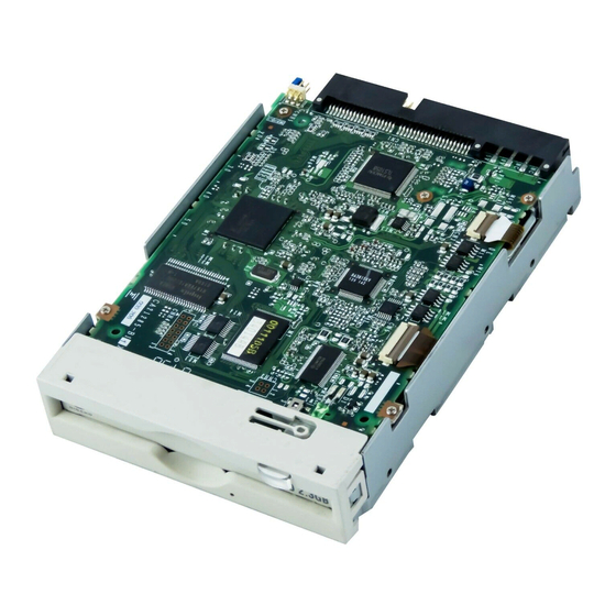
General Description 1.2 Drive Configuration 1.2.1 Drive model Figures 1.1 and 1.2 show the outer view. Figure 1.1 Outer view (with panel) Figure 1.2 Outer view (without panel) C156-E205-01EN... -
Page 33: Figure 1.3 Optical Disk Drive Configuration
1.2.2 Configuration Figure 1.3 shows the drive configuration. The drive consists of mechanical sections, a fixed optics section, actuator, and a control circuit section. The mechanical sections include the spindle motor, actuator section, bias magnet, and the cartridge folder vertical motion mechanism. The fixed optics section consists of the optical components, position detector, and LD controller. -
Page 34: Figure 1.4 Control Circuit Section Block Diagram
General Description The positioner is driven by a linear voice coil motor. A pulse-width modulation (PWM) is adopted as a driving system and realizes low power consumption and high-speed access. (4) Separate optical sections The optical head section is separated in such a way that the fixed optics section is separated from the moving optics section to minimize seek time and positioning error. - Page 35 The control circuit section is divided into two parts: an ATAPI controller section which deals with control between the ATAPI interface and drive interface, and a drive circuit section which controls the drive. (1) ATAPI controller circuit section The ATAPI controller circuit's reliability is improved by large-scale integrated circuit technology.
-
Page 36: Figure 1.5 System Configuration With One Optical Disk Drive
General Description 1.3 System Configuration Figures 1.5 and 1.6 show the PC AT interface system configuration. The interface can be directly connected to the 40-pin AT-compatible IDE interface. Host system AT bus (Host interface) Figure 1.5 System configuration with one optical disk drive Host system AT bus (Host interface) -
Page 37: Chapter 2 Specifications
2.1.1 Model and product number Table 2.1 lists the model and order number. Table 2.1 Model and order number Model Name Order No. MCJ3230AP CA05890-B501 CA05890-B701 CA05890-B601 Note: The panel colors (2.5Y 7.2/0.4) are indicated in Munsell symbols. (JIS Z8721) -
Page 38: Drive Specifications
Specifications 2.1.2 Drive specifications Table 2.2 lists MCJ3230AP drive specifications Table 2.2 Specifications (1 of 2) [MCJ3230AP] Item Optical disk cartridge 128 MB media Total capacity Unformatted 181 MB Formatted 128 MB Capacity/track Unformatted 18,100 bytes Formatted 12,800 bytes Capacity/sector Unformatted... - Page 39 Table 2.2 Specifications (2 of 2) [MCJ3230AP] Item Optical disk cartridge 128 MB media Density 24,424 bpi (1.04µm/bit) 15,875 tpi Loading time (*3) 8 sec. (typ) Unloading time (*4) 4 sec. (typ) Load/unload life 20,000 Host interface ATAPI (ATA/ATAPI-4 standard)
-
Page 40: Table 2.3 Environmental And Power Requirements
(5 to 500 Hz, sine sweep AV record/play) Shock 19.6 m/s (10ms, half-sine pulse) 9.8 m/s (5 to 500 Hz, sine sweep) Shock 49 m/s (10 ms, half-sine pulse) Shock 490 m/s (10 ms, half-sine pulse) Requirement: Packing conditions specified by Fujitsu C156-E205-01EN... -
Page 41: Error Rate
For details, refer to section 3.1.3 'Air Flow' 1. Current limiter value for +5 VDC power: 5 A or less 2. Specifications under transporting condition are under the packaging specified by Fujitsu. 3. A voltage drop may occur depending on the used power supply or power cable. - Page 42 Specifications 2.1.5 Reliability (1) Mean time between failures (MTBF) The MTBF is 120,000 hours or more. Failure due to disk errors is not included. Conditions Power-on time: 200 hours/month or less LD-on time: 20% or less of power-on time Environment Temp.: 25°C Note: The MTBF is defined as follows: total operating time in all fields (hours)
-
Page 43: Table 2.4 Recommended Optical Disk Cartridge Specifications
2.2 Optical Disk Cartridge Specifications 2.2.1 Recommended optical disk cartridge specifications The following three disk types comply with the specifications. Table 2.4 shows the specifications of the optical disk cartridge recommended for this optical disk drive. The use of another disk cartridge may lower drive performance. -
Page 44: Figure 2.1 Optical Disk Cartridge
Specifications 2.2.2 Optical disk cartridge Figure 2.1 shows an optical disk cartridge. The figure below shows the cartridge with its shutter open. Shutter closed 2) Shutter Shutter open Figure 2.1 Optical disk cartridge 1) Cartridge case 3) Write protect tab 4) Disk 5) Hub C156-E205-01EN... - Page 45 The following explains the components of the optical disk drive shown in Figure 2.1: 1) Cartridge case Covers the disk to protect it from damage when handled and facilitates disk replacement. The cartridge case is labeled and has a write protect tab. 2) Shutter Protects the disk against dust.
-
Page 46: Table 2.5 Disk Specifications
Specifications 2.2.3 Disk specifications (1) 128 MB disk The ISO/IEC10090 defines 128 MB disk specification. (2) 230 MB disk The ISO/IEC13963 defines 230 MB disk specification. (3) 540 MB/640 MB disk The ISO/IEC15041 defines 540 MB/640 MB disk specification. (4) 1.3 GB disk The Cherry Book defines 1.3 GB disk specification. -
Page 47: Defect Management Schematic Diagram
2.3 Defect Management 2.3.1 Defect management schematic diagram Defective sectors on the disk shall be replaced by good sectors according to the defect management scheme as follows: Defective sectors found during surface certification are handled by a sector slipping algorithm. Defective sectors found after initialization are handled by a linear replacement algorithm. -
Page 48: Figure 2.3 Example Of Alternate Processing
Specifications Figure 2.3 Example of alternate processing 2-12 C156-E205-01EN... -
Page 49: Temperature Measurement Point
CHAPTER 3 Installation Requirements 3.1 Environmental Requirements 3.2 Mounting Requirements 3.3 Power supply Requirements 3.4 Cable Connections 3.5 Jumper Settings 3.6 Notes on Drive Handling 3.7 Mounting 3.8 Cable Connections 3.9 Operation Confirmation and Preparation for Use after Installation 3.10 Dismounting Drive This chapter describes environmental, mounting, power supply, and connection requirements. -
Page 50: Figure 3.1 Surface Temperature Measurement Points
Installation Requirements (a) Inside optical disk cartridge Hole for inserting thermocouple (b) IC (controller, read amp) IC (controller) IC (power amp) Figure 3.1 Surface temperature measurement points Operating of inner partition wall Tip of thermocouple IC (read amp) C156-E205-01EN... -
Page 51: Temperature Requirements And Measuring Method
3.1.2 Temperature requirements and measuring method Table 3.1 shows the temperature requirement at each measurement point shown in Figure 3.1. Table 3.1 Temperature requirements at measurement points Measurement point Cartridge inside IC (controller) surface IC (read amp.) surface IC (power amp.) surface Following procedure is for temperature measurement of inside cartridge. -
Page 52: Temperature Rise Under Several Conditions
Installation Requirements 3.1.4 Temperature rise under several conditions Table 3.2 Temperature at each measuring point (Reference) [Ambient atmospheric temperature of the optical disk drive: 45°C] Measurement point Inside cartridge IC (controller) surface IC (read amp.) surface IC (power amp.) surface Thermal sensor Notes: The above data are data estimated as they were measured where the... -
Page 53: Mounting Requirements
3.2 Mounting Requirements 3.2.1 External dimensions Figures 3.2 to 3.3 show the dimensions of the drive and the positions of the mounting holes. C156-E205-01EN 3.2 Mounting Requirements... -
Page 54: Figure 3.2 Dimensions
Installation Requirements Unit: mm Figure 3.2 Dimensions C156-E205-01EN... -
Page 55: Figure 3.3 Dimensions (Without Panel)
3.2 Mounting Requirements Unit: mm Figure 3.3 Dimensions (without panel) C156-E205-01EN... -
Page 56: Figure 3.4 Installation Directions
Installation Requirements 3.2.2 Installation direction Figure 3.4 shows the permissible installation directions for this drive. The mounting angle tolerance must be within -5 to 10 from the horizontal. (-) shows that the insertion faces below. " Horizontal Disk insertion slot Manual eject hole "... -
Page 57: Figure 3.5 Centers Of Gravity
3.2 Mounting Requirements 3.2.3 Centers of gravity Figure 3.5 shows the centers of gravity of the drive. Figure 3.5 Centers of gravity C156-E205-01EN... -
Page 58: Figure 3.6 Mounting Frame Structure
Installation Requirements 3.2.4 Notes on mounting (1) Mounting frame structure and clearance a) For vibration resistance and heat dissipation, this optical disk drive uses an embossed structure as shown in Figure 3.6, as well as a frame which has a construction similar to other frames which perform the same function. -
Page 59: Figure 3.7 Service Clearance
(2) Panel function processing When installed in a cabinet, do not change the panel formal. The processing is installation status and the disk insertion door can be closed from any locations. (3) Service clearance Figure 3.7 shows locations which must be accessed for installation and maintenance. -
Page 60: Figure 3.8 Current Waveform (+5 Vdc)
Installation Requirements (7) System ground The optical disk drive should be grounded to the signal ground (SG) of the power supply of the system. This SG line should be supplied with the system. The Frame Ground is shorted in the optical disk drive by a metal strip attached to the vibration isolation rubber between the frame (FG) and the base (SG). -
Page 61: Cable Connections
3.4 Cable Connections 3.4.1 Drive connectors The optical disk drive (ODD) has connectors. Figure 3.9 shows the location of the connectors. " AT interface connector (40-pin) and power supply connector (4-pin) 1 pin Figure 3.9 Connector and terminal locations Power supply connector +12 VDC or not connected +12 VDC RETURN (GND) or not connected +5 VDC RETURN (GND) -
Page 62: Drive Connection
3.4.3 Drive connection Figure 3.10 is a diagram showing cable connections between equipment. Host system Figure 3.10 Cable connection diagram 3-14 Name Model name FCN-707B040-AU/B 445-248-40 1-480424-0 170121-4 AWG18 DC power ODD1 ODD2 Vendor Fujitsu Fujitsu SPECTRS STRIP Power supply C156-E205-01EN... -
Page 63: Mode Setting
3.5 Jumper Settings 3.5.1 Jumper settings at factory shipping Figure 3.11 shows jumper settings at factory shipping. 5-6 short-circuited: Sets the master device. Figure 3.11 Jumper settings at factory shipping 3.5.2 Mode setting (1) Setting master device mode Figure 3.12 shows the setting for recognizing the master device (device 0). Figure 3.12 Master device setting C156-E205-01EN CNH5... -
Page 64: Figure 3.13 Slave Device Setting
Installation Requirements (2) Setting slave device mode Figure 3.13 shows the setting for recognizing the slave device (device 1). Figure 3.13 Slave device setting (3) Setting cable select mode Figure 3.14 shows the master device/slave device setting when the CSEL signal is connected to the interface. -
Page 65: Figure 3.15 Cable Select Examples
CSEL conductor Host system CSEL conductor Host system Figure 3.15 Cable select examples C156-E205-01EN Master device Example 1 Open Slave device Example 2 3.5 Jumper Settings Open Slave device Master device 3-17... -
Page 66: Notes On Drive Handling
Installation Requirements 3.6 Notes on Drive Handling (1) General notes Note the following points to maintain drive performance and reliability: Device damage: 1) Shock or vibration applied to the drive that exceeds the values defined in the standard damage the drive. Use care when unpacking. - Page 67 (3) Installation a) Do not connect or disconnect the connectors or change the terminal settings when the power is on. b) Do not move the drive with the power on. c) Eject the optical disk cartridge, lock the carriage securing the head, turn off the power, then move the drive.
- Page 68 Installation Requirements Desiccant MCJ3230AP Conductive bag Eject pin (use a sealing tape) Shipping Label (2) Master carton (12/24 units) Single-unit packing (5) Transportation a) Transport the optical disk drive packed in principle, with the UP sign upward. b) After unpacking, minimize the transportation distance and use cushions to avoid shock and vibration.
-
Page 69: Checks Before Mounting The Drive
3.7 Mounting 3.7.1 Checks before mounting the drive Before mounting the optical disk drive in the system cabinet, check whether the jumper settings are set correctly. 3.7.2 Mounting procedure How the drive is mounted depends on the system cabinet structure. Determine the mounting procedure in consideration of the requirements of each system. -
Page 70: Operation Confirmation And Preparation For Use After Installation
Installation Requirements 1) Make sure that the system power is off. 2) Do not connect or disconnect any cable when the power is on. 1) Connect the DC ground cable (only if required to decrease ground noise). 2) Connect the power cables. 3) Connect the AT interface cable. -
Page 71: Dismounting Drive
The BUSY LED is on while the optical disk drive is executing seek, write, or read operations. The BUSY LED is on momentarily, so it seems as if it blinked or is off. The eject motor turns once when the power is turned on so that in case the spindle motor position deviates due to shocks received by the drive during transport the position is corrected to allow the cartridge to be inserted normally. - Page 72 Installation Requirements 4) Remove the four screws securing the drive, then remove the drive from the system cabinet. 5) When storing or transporting the drive, put the drive into an antistatic bag. (See Section 3.6.) 3-24 C156-E205-01EN...
-
Page 73: Chapter 4 Host Interface
CHAPTER 4 Host Interface 4.1 Pin Assignment 4.2 Signal Description 4.3 Interface Registers 4.4 Various Processes 4.5 ATA Commands 4.6 Packet Commands 4.7 Timing This chapter describes host interface specification. C156-E205-01EN... -
Page 74: Pin Assignment
Host Interface 4.1 Pin Assignment The table below lists pin assignments of the interface connector. Table 4.1 Connector pin assignments (1/2) Description Reset Ground Data bus bit 7 Data bus bit 8 Data bus bit 6 Data bus bit 9 Data bus bit 5 Data bus bit 10 Data bus bit 4... - Page 75 Table 4.1 Connector pin assignments (2/2) Ground I/O Ready DMA ready during Ultra DMA data out bursts Data strobe during Ultra DMA data in bursts Cable Select DMA Acknowledge Ground Interrupt Request 16 Bit I/O Device Address Bit 1 PASSED DIAGNOSTICS Cable assembly type identifier Device Address Bit 0 Device Address Bit 2...
-
Page 76: Table 4.2 Signal Description
Host Interface 4.2 Signal Description Table 4.2 Signal description (1/2) Signal name RESET- 3, 5, 7, 9, 11, DD7-0 13, 15, 17, 18, DD15-8 16, 14, 12, 10, 8, 6, 4 DMARQ DIOW- STOP DIOR- HDMARDY- HSTROBE IORDY DDMARDY- DSTROBE CSEL DMACK- INTRQ... - Page 77 Table 4.2 Signal description (2/2) Signal name CS0- CS1- DASP- 2, 19, 22, 24, Ground 26, 30, 40 C156-E205-01EN Description Select signal used to select the command block register Select signal used to select the control block register When reset, slave (device 1) output signal indicating that the slave (device 1) exists.
-
Page 78: Interface Registers
Host Interface 4.3 Interface Registers 4.3.1 I/O registers This section provides the I/O register functions and mapping. Definitions of each register vary depending on which ATA or ATAPI commands are used. Table 4.3 I/O port functions and mapping Address signal CS0- CS1- The letter A indicates that the bit is asserted, N indicates that the bit is negated,... -
Page 79: Ata Command Register
4.3.1.1 Alternate Status register This register contains the same information as that of the ATAPI Status register, except that the ODD does not recognize interrupts when reading this register. Therefore, the ODD does not clear the INTRQ signal and does not clear interrupts during the pending. -
Page 80: Table 4.6 Bit Definitions Of Drive Address Register
Host Interface 4.3.1.5 Drive Address register This register's bits are defined as shown below. Table 4.6 Bit definitions of Drive Address register nWTG nHS3 HiZ is always in the high-impedance state. nWTG indicates the status of the ODD internal data write control signal (Write Gate). -
Page 81: Table 4.8 Bit Definitions Of Atapi Block Device Select Register
4.3.1.7 ATAPI Block Device Select register This register's bits are defined as shown below. Table 4.8 Bit definitions of ATAPI Block Device Select register Unused Unused Unused Bits 7, 6, 5, 3, 2, 1, and 0 are not used. The ODD ignores all value sets in these bits. -
Page 82: Ata Sector Count Register
Host Interface 4.3.1.9 ATA Features register This register is used for the SET FEATURES command. 4.3.1.10 ATAPI Features register This register's bits are defined as shown below. Table 4.10 Bit definitions of ATAPI Features register Reserved All values in bits 7 to 2 are ignored. OVERLAP is not used. -
Page 83: Sector Number Register
Packet command transfer Data or parameter transfer (from the ODD to the host) Data or parameter transfer (from the host to the ODD) The completion status in the Status register is effective. 4.3.1.13 Sector Number register This register is not used. The ODD ignores all specified values. 4.3.1.14 ATAPI Status register This register indicates the status of the ODD. - Page 84 Host Interface The ODD sets BSY: a) After RESET- is negated or within 400 ns of setting the SRST bit of the Device Control Register b) Within 400 ns of receiving a command when the DRQ bit is not set c) Between data transfer blocks of the PIO data-in/PIO data-out command when the DRQ bit is not set d) After data block transfer with the PIO data-out command when the DRQ...
-
Page 85: Various Processes
4.4 Various Processes 4.4.1 Reset response There are four types of resets. Power-on reset " The ODD performs initialization such as initial diagnostics and default setting. If any media is mounted, it also spins up media. Hardware reset " The ODD is reset when the RESET- signal is asserted. The ODD initializes the interface controller by setting default values. -
Page 86: Automatic Alternate Sector Assignment Function
Host Interface " UNIT ATTENTION is not generated. " The contents set with the MODE SELECT and Set Feature commands remain unchanged. 4.4.2 Signature The ODD specifies the following as signatures that indicate the support of the PACKET command function in the task file. Sector Count = 01h Sector Number = 01h Cylinder Low = 14h... -
Page 87: Cache Function
After automatic alternate assignment terminates successfully, the ODD does not report any error. 4.4.5 Cache function The ODD supports the read cache and MO write cache. The read cache consists of the read ahead cache and the LRU cache that reads write data remaining in the data buffer. -
Page 88: Media Status Notification Function
Host Interface without reading it from media. If the cache is hit with a read command, the ODD makes the data in the hit segment being kept in the highest priority. The data listed below cannot be stored in the read cache. Data read before power-off Data already stored before media is mounted All buffer data is discarded under the following conditions:... -
Page 89: Power Mode
The GET MEDIA STATUS command is enabled. The Eject switch is disabled. The media status notification function is disabled at power-on reset, software reset, when the DEVICE RESET command is received, or when the EXECUTE DEVICE DIAGNOSTIC command is received. 4.4.7 Power management function The ODD provides the power management function that minimizes the power consumed. -
Page 90: Standby Timer
Host Interface 4.4.7.4 Idle mode In idle mode, the servo and read/write circuits stop. The ODD can receive a command from the host, but because some circuits stop, the ODD takes 1 s seconds (standard) to access media. If no command is issued within a specified time (180 s) in active mode, the ODD automatically enters pre-idle mode, then enters idle mode. -
Page 91: Unsupported Functions
4.4.7.8 Power mode transition The power mode transits as shown in Figure 4.1. inserted. Media is (1) The ODD enters idle mode because it receives the Idle Immediate command or because it receives no commands within a specified time. (2) The ODD enters idle mode with the Idle Immediate command. (3) The ODD enters standby mode with the Standby Immediate command and standby timer. -
Page 92: Led Indications
Host Interface The ODD also does not support the following functions which are not supported by ATAPI devices. SMART feature set Host Protected Area feature set 4.4.9 LED Indications The ODD notifies the operator of a serious error by turning on or blinking the LED lamp. -
Page 93: Ata Commands
4.5 ATA Commands Table 4.17 lists supported ATA commands. This section represents ODD registers as shown below. Cylinders High/Low registers: CY Sector register: SC Device/Head register: DH Sector Number register: SN Features register: FR Table 4.17 Command codes and parameters Protocol Command name CHECK POWER MODE... -
Page 94: Check Power Mode (E5H)
Host Interface ND - A non data command PI - A PIO data-in command 4.5.1 CHECK POWER MODE (E5h) Table 4.18 CHECK POWER MODE command The CHECK POWER MODE command sets the ODD power mode status in the SC register, then notifies the host of the value in Table 4.19 When the drive is in sleep mode, the interface is inactive and the ODD cannot receive this command. -
Page 95: Execute Device Diagnostic (90H)
4.5.2 DEVICE RESET (08h) Table 4.20 DEVICE RESET command The DEVICE RESET command resets the ODD. When the ODD receives the DEVICE RESET command, it sets the BSY bit to 1. After reset is completed, the ODD sets the BUSY bit to 0. INTRQ is not asserted. 4.5.3 EXECUTE DEVICE DIAGNOSTIC (90h) Table 4.21 EXECUTE DEVICE DIAGNOSTIC command When the ODD receives this command, it recognizes self-diagnostics. -
Page 96: Self-Diagnosis Detailed Code
Host Interface When the ODD receives this command, it responds to the command regardless of the DEV bit value; this means that the drive is unit 0 or 1. When the ODD is device 0 (master), its response after the command is received depends on whether device 1 (slave) is connected. -
Page 97: Get Media Status (Dah)
4.5.4 FLUSH CACHE (E7h) Table 4.23 FLUSH CACHE command The FLUSH CACHE command writes unwritten data in the cache memory in the data buffer to the media. 4.5.5 GET MEDIA STATUS (DAh) Table 4.24 GET MEDIA STATUS command The GET MEDIA STATUS command respond with the ODD status. The command ends abnormally in either of the conditions given below and sets the value shown in Table 4.25 in the Error register. -
Page 98: Identify Packet Device (A1H)
Host Interface When the Eject switch is pressed When media is write-protected Otherwise, the command ends normally. If a hardware error by which the command cannot be executed occurs, as is the case with other commands, the command ends with Aborted Command. Bit 7 Bit 6 Bit 5... -
Page 99: Table
15-14 12-8 0000h 10-19 "xxx...xxx" 20-22 0000h 23-26 "aaab" 27-46 “FUJITSU MCJ3230AP” 47-48 0000h 0F00h C156-E205-01EN Description General configuration information Protocol type (10b = ATAPI device) Reserved Device type 00000b = Direct access unit Replaceable media device 1b CMD DRQ type (10b = Accelerated DRQ) -
Page 100: Table
Host Interface Table 4.27 Device parameter information (2/6) Word Value Bits 0000h 0200h 15-8 0000h 15-0 0007h 15-3 54-62 0000h 0407h (Default value) 0003h 15-2 0078h (120) 0078h (120) 0078h (120) 0078h (120) 69-70 0000h 07D0h (2000) 0000h (0000) 73-79 0000h 4-28 Description... -
Page 101: Table
Table 4.27 Device parameter information (3/6) Word Value Bits 0020h 0015h 4278h 4010h 13-8 4000h C156-E205-01EN Description Major Version number (ATA/ATAPI-5) Minor Version number (ATA/ATAPI-5 T13 1321D revision 1) Command set supported (A value of less than 1 indicates that the command is supported.) Unused (0b) NOP command (1b) READ BUFFER command (0b) -
Page 102: Table
Host Interface Table 4.27 Device parameter information (4/6) Word Value Bits 13-0 4278h (Default value) 0000h (Default value) 15-8 4-30 Description Reserved (0b) Command set supported and whether the function is enabled or disabled (A value of less than 1 indicates that the command is supported and enabled.) Unused (0b) NOP command support (1b) -
Page 103: Table
Table 4.27 Device parameter information (5/6) Word Value Bits 4000h 13-0 0007h 15-13 (Default value) 89-92 0000h xxxxh 12-8 C156-E205-01EN Description Command set supported and whether the function is enabled or disabled (A value of less than 1 indicates that the command is supported and enabled.) Reserved Reserved (0b) -
Page 104: Table
Host Interface Table 4.27 Device parameter information (6/6) Word Value Bits 10-9 94-126 0000h 0001h 15-2 0000h 15-9 129- 0000h 0000h 15-8 4-32 Description - for device 1 If PDIAG- is asserted: 1b If not: 0b Reserved Reserved (0b) Media status notification function supported (01b) Reserved (0b) Security level (0b) Reserved (0b) -
Page 105: Idle Immediate (E1H)
4.5.7 IDLE IMMEDIATE (E1h) Table 4.28 IDLE IMMEDIATE command The ODD sets the power mode to idle mode. 4.5.8 NOP (00h) The NOP command enables 16-bit access for Status register checking. The ODD judges an unsupported command. The command ends with Aborted Command. C156-E205-01EN Table 4.29 NOP command 4.5 ATA Commands... -
Page 106: Packet (A0H)
Host Interface 4.5.9 PACKET (A0h) The PACKET command issues the ATAPI packet command. For the Byte Count Limit, specify the maximum number of bytes transferred per INTRQ in PIO mode. When the value of the Byte Count Limit is smaller than 2048, the data is transferred in 2048-byte units. -
Page 107: Set Features (Efh)
4.5.10 SET FEATURES (EFh) Table 4.31 SET FEATURES command The SET FEATURES command changes the ODD operating mode to the mode set in the SC and FR registers. If the specified value is not supported by the ODD or an invalid value, the ODD reports Aborted Command. Table 4.32 FR register setting value Setting value... -
Page 108: Transfer Setting Values In The Sc Register
Host Interface Table 4.33 Transfer setting values in the SC register Transfer mode PIO default transfer mode PIO default transfer mode (without IORDY signal) PIO flow control transfer mode (with IORDY signal) Undefined Multiword DMA transfer mode Ultra DMA transfer mode Undefined Mode indicates the number of transfer modes. -
Page 109: Sleep (E6H)
4.5.11 SLEEP (E6h) The SLEEP command sets the ODD in sleep mode. The ODD enters sleep mode by following the steps given below. 1. The ODD spins down media. 2. The ODD issues an interrupt to the host to report command end. After the host receives the interrupt, the ODD deactivates the interface. -
Page 110: Standby Immediate (E0H)
Host Interface 4.5.12 STANDBY IMMEDIATE (E0h) Table 4.37 STANDBY IMMEDIATE command The ODD sets the power mode to standby mode. 4-38 C156-E205-01EN... -
Page 111: Packet Commands
4.6 Packet Commands The ODD supports the packet commands listed below. Table 4.38 Packet command codes and parameters Command ERASE (10) FORMAT UNIT INQUIRY MODE SELECT (6) MODE SELECT (10) MODE SENSE (6) MODE SENSE (10) PREVENT/ALLOW MEDIUM REMOVAL READ (10) READ CAPACITY READ FORMAT CAPACITIES READ DEFECT DATA (10) -
Page 112: Erase Command
Host Interface In this chapter, unless otherwise specified, the value of data marked as "Reserved" that is sent from the host is ignored. In addition, unless otherwise specified, 0 is returned to the data marked as "Reserved" that is sent from the device to the host. However, if the data marked as "Reserved"... -
Page 113: Format Unit Parameter List
4.6.2 FORMAT UNIT command Table 4.40 FORMAT UNIT command Byte Reserved 5-11 The FORMAT UNIT command formats media physically on the basis of the specified parameter values. When the FmtData bit is 1, the FORMAT UNIT parameter list must be transferred. -
Page 114: Inquiry Command
Host Interface When the IMMED (Immediate) bit is 1, the ODD responds with immediate end after the command is received and before formatting is completed. At this time, during formatting, the Ready bit of the Status register is set to 0, and then set to1 after formatting is completed. -
Page 115: Inquiry Data
Response data format (2h) Additional length (2Bh) Reserved Vendor Information "FUJITSU" (in ASCII) Products Identification "MCJ3230AP" (in ASCII) Firmware Revision Level "0000" - "999z" (in ASCII) Firmware Local Revision 00h - FFh (in HEX) Boot Firmware Revision Level 00h - FFh (in HEX) Signature "MO"... -
Page 116: Table
Host Interface 4.6.4 MODE SELECT (6) command Table 4.45 MODE SELECT (6) command Byte Reserved 9-11 The MODE SELECT (6) command sets various device operating modes. The PF (Page Format) bit must be 1. If the PF bit is 0, the command responds with Check Condition. -
Page 117: Mode Parameter Header
Table 4.47 lists the mode parameter list. Byte The mode parameter list consists of a mode parameter header Block Descriptor and Mode Page (s). Table 4.48 lists the mode parameter header. Table 4.48 Mode parameter header Byte The values specified for Mode Data Length, Medium Type Code, and WP are ignored. -
Page 118: Read-Write Error Recovery Page
Host Interface Table 4.50 lists the Mode Page format. Byte 4.6.4.1 Read-Write error recovery page Table 4.51 Read-Write error recovery page Byte PS (1) AWRE Reserved 9-11 When the AWRE (Automatic Write Reallocation Enable) bit is 0, no automatic alternate block assignment is made for the WRITE (10), or WRITE AND VERIFY command. -
Page 119: Changeable Values In The Read-Write Recovery Page
RECOVERED ERROR is reported: When 7 to 8 error bytes per interleaving was corrected by the ECC correction during read operation When a defect sector is detected and replaced with an alternate sector during a write operation When an error occurs in one of four sets of media data during media management information (DMA) write operation with the FORMAT UNIT command (MEDIUM ERROR is set if an error occurs in two, three, or four sets of four sets.) -
Page 120: Flexible Disk Page
Host Interface 4.6.4.2 Flexible disk page Byte 10-19 21-27 28-29 30-31 This page is supported for compatibility of device driver. Recommendation: A device driver should not be used this page, because if device driver uses of this page and it is not able to keep compatibility for logically of media (No guarantee). -
Page 121: Table 4.55 Changeable Values In Flexible Disk Page
Table 4.55 Changeable values in flexible disk page Byte 10-19 21-27 28-29 30-31 Table 4.56 Default values in flexible disk page Byte In case of 640 Mbytes, 1.3 Gbytes and 2.3 Gbytes media = 800h In case of Not Ready = the value of the maximum capacity media among the 10-19 21-27 28-29... -
Page 122: Table 4.58 Changeable Values In The Caching Page
Host Interface 4.6.4.3 Caching page Byte PS (1) 3-19 When the WCE (Write Cache Enable) bit is 0, the write cache function for the WRITE (10), or WRITE AND VERIFY command is disabled. When the bit of WCE is 1, the write cache function is enabled. When the RCD (Read Cache Disable) bit is 0, the read ahead cache function for the READ (10) command is enabled. -
Page 123: Table 4.61 Power Condition Page Variable
4.6.4.4 Power Condition page Table 4.60 Power Condition Page Byte PS (1) 8-11 The values specified for the Idle bit and Idle Condition Timer are ignored. It always operates in accordance with the default timer value in the ODD. When the Standby bit is 1, specify the time after the device enters idle mode until it enters standby mode. -
Page 124: Table 4.62 Power Condition Page Default Value
Host Interface Table 4-62 Power Condition Page Default value Byte 8-11 4.6.4.5 Verify Control Page Table 4-63 Verify Control Page Byte PS (1) Reserved The Verify Control Page is a vendor unique page. When the Audio Visual Mode (AV) bit is 0, the cache mode is applied. When the AV bit is 1, the AV data support mode is applied. -
Page 125: Table 4.66 Verify Control Page Default Value
The DevType specifies the Device Type value that is provided in response to the Identify command and the Identify Packet Device command. To validate the specified value, instruct the system to save the specification, and power on again. The Verify Control Page can be saved. Table 4.65 Verify Control Page variable Byte Table 4.66 Verify Control Page default value... -
Page 126: Table 4.69 Mode Parameter Header
Host Interface For information about the supported mode page, see Table 4.46, Mode Page Codes. Table 4.68 shows the Mode Parameter List. Table 4.68 Mode Parameter List Byte The Mode Parameter List consists of the Mode Parameter Header, the Block Descriptor, and the Mode Page. -
Page 127: Table 4.70 Mode Sense (6) Command
4.6.6 MODE SENSE (6) command Table 4.70 MODE SENSE (6) command Byte Reserved 5-11 The MODE SENSE (6) command transfers the mode parameter list to the host. When the Disable Block Descriptors (DBD) is 1, the Block Descriptor is not returned. -
Page 128: Table 4.73 Mode Parameter Header
Host Interface Byte The mode parameter list consists of a mode parameter header and Block Descriptor and Mode Page. The mode parameter header is shown in Table 4.73. Table 4.73 Mode parameter header Byte Medium Type Code returns the following values: 03h for non overwrite 07h for overwrite 03h for other media and Not Ready state... -
Page 129: Table 4.76 Mode Sense (10) Command
Byte Each field value of the Block Descriptor is validated only when the accessible media is inserted. If not, 0 is returned. Table 4.75 shows the mode page format. Byte A value of 1 in PS indicates that the page descriptor can be saved on the Flash ROM. -
Page 130: Table 4.78 Mode Parameter Header
Host Interface The MODE SENSE (10) command performs the same processing as the MODE SENSE (6) command. For an explanation of each field, see Section 4.6.6, MODE SENSE (6) command. Table 4.77 shows the mode parameter list. Table 4.77 Mode Parameter List Byte The Mode Parameter List consists of the Mode Parameter Header, the Block Descriptor, and the Mode Page. -
Page 131: Prevent/Allow Medium Removal Command
4.6.8 PREVENT/ALLOW MEDIUM REMOVAL command Table 4.79 PREVENT/ALLOW MEDIUM REMOVAL command Byte 5-11 The PREVENT/ALLOW MEDIUM REMOVAL command allows or inhibits media ejection on the device. A value of 0 in the Prevent bit allows ejection and a value of 1 disables ejection. The power-on default value is Enabled. -
Page 132: Table 4.82 Read Capacity Command
Host Interface 4.6.9 READ (10) command Table 4.81 READ (10) command Byte 9-11 The READ (10) command reads data for the specified number of blocks from the specified logical block address and transfers it. Logical Block Address specifies the head logical block address used to start reading. -
Page 133: Table 4.85 Read Format Capacities Data Format
Table 4.83 READ CAPACITY data Byte Last Block Address specifies LBA of the last accessible block. Block Length in Bytes indicates the number of bytes per block. 4.6.11READ FORMAT CAPACITIES command Table 4.84 READ FORMAT CAPACITIES command Byte 9-11 The READ FORMAT CAPACITIES command transfers data on the capacity of media currently loaded to the host. -
Page 134: Table 4.87 Current/Maximum Capacity Descriptor
Host Interface Capacity List Length indicates the length of the capacity descriptor in bytes. Table 4.87 Current/Maximum capacity descriptor Byte Number of Blocks indicates the number of addressable blocks. Descriptor Code indicates the type of descriptor to be reported to the host. Block Length indicates the length of the block in bytes. -
Page 135: Table 4.90 Defect List Format - Read Defect Data (10)
The READ DEFECT DATA command transfers media defect data to the host. When Plist is 1, the command transfers header and PDL. When Glist is 1, this command transfers header and SDL. When both Plist and Glist are 0, it transfers the header. -
Page 136: Table 4.95 Defect List Format - Read Defect Data (12)
Host Interface Table 4.93 Sector Address Format Byte For disks other than 2.3 GB: 00b For 2.3-GB disks: 00b Groove 10b Land 4.6.13 READ DEFECT DATA (12) command Table 4.94 READ DEFECT DATA (12) command Byte Reserved 10-11 The READ DEFECT DATA (12) command transfers the defect data to the host. When Plist is 1, the command transfers header and PDL. -
Page 137: Table 4.96 Defect List Header - Read Defect Data (12)
Table 4.96 Defect List Header - READ DEFECT DATA (12) Byte 4.6.14 READ LONG command Table 4.97 READ LONG command Byte 9-11 The READ LONG command reads data in the data, CRC, and ECC sections from the specified logical block address. The transfer byte length must be a multiple of 600 (258h) bytes for 512 byte media and a multiple of 2380 (94Ch) bytes for 2048 byte media. -
Page 138: Table 4.98 Receive Diagnostic Results Command
Host Interface 4.6.15 RECEIVE DIAGNOSTIC RESULTS command Table 4.98 RECEIVE DIAGNOSTIC RESULTS command Byte 5-11 The RECEIVE DIAGNOSTIC RESULTS command transfers the diagnostic results indicated by the SEND DIAGNOSTIC command to the host. The RECEIVE DIAGNOSTC RESULT command must be issued following the SEND DIAGNOSTIC command. -
Page 139: Table 4.100 Request Sense Data
When the ODD detects a CRC error involving the Ultra DMA transfer during the data transfer using this command, it returns the CHECK CONDITION. (The Sense Key of the Error register indicates ABORTED COMMAND.) The original sense data at the CRC error occurrence is reported normally using the REQUEST SENSE command. -
Page 140: Table 4.103 Logical Block Address Format
Host Interface Sense Key outlines the error. The definition of Sense Key is listed in Table 4.102. Sense Key Abbreviation NO SENSE RECOVERED ERROR NOT READY MEDIUM ERROR HARDWARE ERROR ILLEGAL REQUEST UNIT ATTENTION DATA PROTECT BLANK CHECK 9h-Ah Reserved ABORTED COMMAND Ch-Fh... -
Page 141: Table 4.104 Asc/Ascq List (1/2)
Additional Sense Code (ASC)/Additional Sense Code Qualifier (ASCQ) indicates detailed error information. The definition of ASC/ASCQ is shown in Table 4.104. Table 4.104 ASC/ASCQ list (1/2) Sense ASCQ LOGICAL UNIT NOT READY, CAUSE NOT REPORTABLE LOGICAL UNIT NOT READY, FORMAT IN PROGRESS TRACK FOLLOWING ERROR LOGICAL UNIT COMMUNICATION CRC ERROR TRACKING SERVO ERROR... -
Page 142: Table 4.105 Format Progress Indication Bytes
Host Interface Table 4.104 ASC/ASCQ list (2/2) Sense ASCQ INCOMPATIBLE MEDIUM INSTALLED CANNOT READ MEDIUM/UNKNOWN FORMAT MEDIUM FORMAT CORRUPTED FORMAT COMMAND FAILED NO DEFECT SPARE LOCATION AVAILABLE DEFECT LIST UPDATE FAILURE ROUNDED PARAMETER MEDIUM NOT PRESENT DIAGNOSTIC FAILURE ON COMPONENT NN INTERNAL TARGET FAILURE COMMAND PHASE ERROR DATA PHASE ERROR... -
Page 143: Send Diagnostic Command
4.6.17 SEND DIAGNOSTIC command Table 4.106 SEND DIAGNOSTIC command Byte 5-11 The SEND DIAGNOSTIC command instructs diagnostic operation from the host. When the Self-Test bit is 1, the command executes diagnostics on the data buffer. If an error occurs, the device responds with Check Condition. Parameter List Length specifies the data length of diagnostic parameters to be transferred. -
Page 144: Start/Stop Unit Command
Host Interface 4.6.19 START/STOP UNIT command Table 4.108 START/STOP UNIT command Byte 5-11 The START/STOP UNIT command ejects media or starts and stops rotating the disk. When the IMMED (Immediate) bit is 1, command completion is reported before processing is completed. Processing for other values is listed in Table 4.109. -
Page 145: Synchronize Cache Command
4.6.20 SYNCHRONIZE CACHE command Table 4.110 SYNCHRONIZE CACHE command Byte 9-11 The SYNCHRONIZE CACHE command writes cache memory data not written yet in the data buffer to media. The IMMED (Immediate) bit is not supported. When the IMMED bit is 1, the command responds with Check Condition. -
Page 146: Write (10) Command
Host Interface 4.6.22 VERIFY command Byte 9-11 The VERIFY command verifies for the specified number of blocks from the specified logical block address. Logical Block Address specifies the head logical block address from which verification starts. Verification Length specifies the number of blocks to be verified and transferred. When Verification Length is 0, the command verifies no block and ends normally. -
Page 147: Write And Verify Command
The WRITE (10) command receives and writes data for the specified number of blocks from the specified logical block address. Logical Block Address specifies the head logical block address used to start writing. Transfer Length specifies the number of blocks to be transferred and written. When Transfer Length is 0, the command does not carry out data transfer. -
Page 148: Write Buffer Command
If write operation to the flash ROM ends abnormally, the command responds with Check Condition. If power failure or interface cable disconnection occurs during downloading, flash ROM data may not be assured. Valid download data is Fujitsu distributed data only. 4-76 Operation Code (3Bh) Reserved... -
Page 149: Write Long Command
4.6.26 WRITE LONG command Table 4.116 WRITE LONG command Byte 9-11 The WRITE LONG command writes data in the data, CRC, and ECC sections to the specified logical block address. The transfer byte length must be a multiple of 600 (258h) bytes for 512 byte media and a multiple of 2380 (94Ch) bytes for 2048 byte media. -
Page 150: Timing
Host Interface 4.7 Timing 4.7.1 Register/PIO data transfer timing DA(2:0) CS0-/CS1- DIOR- /DIOW- WRITE DD(15:0) READ DD(15:0) IOCS16- IORDY Figure 4.2 Register/PIO data transfer 4-78 C156-E205-01EN... -
Page 151: Table 4.117 Register/Pio Data Transfer Timing Parameters
Table 4.117 Register/PIO data transfer timing parameters Symbol Timing parameter Cycle time DIOR-/DIOW- setup time DIOR-/DIOW- pulse width DIOR-/DIOW- recovery time DIOW- data setup time DIOW- data hold time DIOR- data setup time DIOR- data hold time DIOR- data High –Z time From address decided to IOCS16- asserted From address decided to IOCS16- released DIOR-DIOW- to address valid hold time... -
Page 152: Multiword Dma Data Transfer Timing
Host Interface 4.7.2 Multiword DMA data transfer timing CS0-/CS1- DMARQ DMACK- DIOR/DIOW- READ DD(15:0) WRITE DD(15:0) Figure 4.3 Multiword DMA data transfer 4-80 C156-E205-01EN... -
Page 153: Table 4.118 Multiword Dma Data Transfer Timing Parameters
Table 4.118 Multiword DMA data transfer timing parameters Symbol Timing parameter Cycle time DIOR-/DIOW- pulse width DIOR- data access time DIOR- data hold time DIOR-/DIOW- data setup time DIOW- data hold time DMACK- to DIOR/DIOW- setup time DIOR-/DIOW to DMACK- hold time DIOR-/DIOW negated pulse width DIOR-/DIOW to DMARQ- delay time CS (1:0) to DIOR /DIOW valid time... -
Page 154: Figure 4.5 Ultra Dma Data In Transfer (Continuous Transfer Timing)
Host Interface 4.7.3 Ultra DMA data in transfer (initialization timing) DMARQ DMACK- tACK STOP tACK HDMARDY DSTROBE DS(15.0) tACK DA(2.0) tACK CS0-,CS1- Figure 4.4 Ultra DMA data in transfer (initialization timing) 4.7.4 Ultra DMA data in transfer (continuous transfer timing) tCYC DSTROBE at device... -
Page 155: Figure 4.7 Ultra Dma Data In Transfer (Device End Timing)
4.7.5 Ultra DMA data in transfer (host stop timing) DMARQ DRMACK- STOP HDMARDY- DSTROBE DD(15:0) Figure 4.6 Ultra DMA data in transfer (host stop timing) 4.7.6 Ultra DMA data in transfer (device end timing) DMARQ DMACK- STOP HDMARDY DSTROBE tZAH DD(15:0) DD(2:0) CS0-, CS1-... -
Page 156: Ultra Dma Data In Transfer (Host End Timing)
Host Interface 4.7.7 Ultra DMA data in transfer (host end timing) DMARQ DMACK- STOP HDMARDY- tRFS DSTROBE DD(15:0) DA(2:0) CS0-, CS1- Figure 4.8 Ultra DMA data in transfer (host end timing) 4-84 tMLI tZAH tMLI tDVS tACK tACK tIORDYZ tDVH tACK tACK C156-E205-01EN... -
Page 157: Figure 4.9 Ultra Dma Data Out Transfer (Initialization Timing)
4.7.8 Ultra DMA data out transfer (initialization timing) DMARQ DMACK- tACK STOP tZIORDY DDMARDY- tACK HSTROBE DD(15:0) tACK DA(2:0) tACK CS0-, CS1- Figure 4.9 Ultra DMA data out transfer (initialization timing) 4.7.9 Ultra DMA data out transfer (continuous transfer timing) tCYC HSTROBE at host... -
Page 158: Ultra Dma Data Out Transfer (Device Stop Timing)
Host Interface 4.7.10 Ultra DMA data out transfer (device stop timing) DMARQ DMACK- STOP DDMARDY- HSTROBE DD(15:0) Figure 4.11 Ultra DMA data out transfer (device stop timing) 4-86 tRFS C156-E205-01EN... -
Page 159: Ultra Dma Data Out Transfer (Host Suspend Timing)
4.7.11 Ultra DMA data out transfer (host suspend timing) DMARQ DMACK- STOP DDMARDY- HSTROBE DD(15:0) DA(2:0) CS0-, CS1- Figure 4.12 Ultra DMA data out transfer (host suspend timing) C156-E205-01EN tMLI tMLI tDVS 4.7 Timing tIORDYZ tACK tDVH tACK tACK 4-87... -
Page 160: Ultra Dma Data Out Transfer (Device End Timing)
Host Interface 4.7.12 Ultra DMA data out transfer (device end timing) DMARQ DMACK- STOP DDMARDY- tRFS HSTROBE DD(15:0) DA(2:0) CS0-, CS1- Figure 4.13 Ultra DMA data out transfer (device end timing) 4-88 tMLI tMLI tDVS tACK tIORDYZ tACK tDVH tACK tACK C156-E205-01EN... -
Page 161: Table 4.119 Ultra Dma Data Out Transfer Parameter
Table 4.119 Ultra DMA data out transfer parameter Symbol Timing parameter t2CYCTYP Average 2-cycle time tCYC Cycle time (for non-target clock and at clock change) t2CYC 2-cycle time (at clock change) Data setup time on receiving side Data hold time on receiving side tDVS Data enabled setup time on sending side tDVH... -
Page 162: Power-On And Reset Timing
Host Interface 4.7.13 Power-on and Reset Timing RESET- Device 0 BSY Device 0 DRDY Device 0 PDIAG-out Device 0 DASP-out Device 0 DASP-in Device 0 PDIAG-in Device 1 BSY Device 1 DRDY Device 1 DASP-out Device 1 PDIAG-out Device 0 sets the BSY bit to 0 when device 1 is not connected. Device 0 uses DASP- to indicate that it is in operation when device 1 is not connected. -
Page 163: Table
Table 4.120 Power-on and reset timing Symbol Timing parameter RESET- pulse width Device 0 RESET- negation to BSY bit set to one, release PDIAG - Device 0 release DASP- Device 0 sample time of DASP- Device 0 sample time of PDIAG- Device 1 RESET- negation to BSY bit set to one Device 1 assert DASP- Device 1 negate PDIAG - if asserted... - Page 164 This page is intentionally left blank.
-
Page 165: Chapter 5 Operation And Cleaning
CHAPTER 5 Operation and Cleaning 5.1 Operating Optical Disk Drive 5.2 Cleaning Drive 5.3 Optical Disk Cartridge Operation 5.4 Cleaning Optical Disk Cartridge This chapter describes how to operate and clean the drive and the optical disk cartridges. 5.1 Operating Optical Disk Drive The drive has an automatic load function. -
Page 166: Figure 5.1 Optical Disk Drive Front View (With Panel)
Operation and Cleaning 5.1.1 Optical disk drive Horizontal Horizontal Disk insertion slot Manual eject hole Vertical (Two orientations) Figure 5.1 Optical disk drive front view (with panel) The following explains the parts and functions of the optical disk drive (the following numbers correspond to the numbers in Figures 5.1): 1) Disk insertion slot Use this slot to insert and eject the optical disk cartridge. -
Page 167: Note
5.1.2 Note To maintain the performance and reliability of the drive, keep the following point in mind: When the drive is in the busy state, do not eject the optical disk cartridge. Particularly, do not manually eject the cartridge by force. Be careful sufficiently not to insert the different drive (etc. -
Page 168: Figure 5.2 Inserting Cartridge
Operation and Cleaning 4) Push the cartridge into the slot until it completes moving below (a little further in than the operator panel). The cartridge remains inserted in the drive. The BUSY LED indicator lamp lights when the drive power is turned on. The cartridge remains inserted in the drive. -
Page 169: Ejecting (Removing) Cartridge
5.1.4 Ejecting (removing) cartridge Remove the cartridge as explained below. (1) When the drive power is on: The cartridge can be removed by pressing the eject button. (See figure 5.3) Notes: 1) If the ATAPI command prevents ejection, the cartridge cannot be removed. -
Page 170: Table 5.1 Head Cleaner
Operation and Cleaning 5.2 Cleaning Drive When a dust or smoke of cigarette is stained to the lens actuator, a performance of whole drive may be down. Clean the lens actuator periodically using following head cleaner. Note: Cleaning period differs depending on the installation condition. Usually, cleaning period is once a three months. -
Page 171: Figure 5.4 Optial Disk Cartridge
5.3 Optical Disk Cartridge Operation 5.3.1 Optical disk cartridge Figure 5.4 shows the optical disk cartridge. For operation and cleaning, users should be familiar with the parts shown in the figure. See Subsection 2.3.2 for the functions of the parts. Shutter closed 2. -
Page 172: Figure 5.5 Write Protect Tab
Operation and Cleaning 5.3.2 Write protect tab Moving the write protect table determines whether to enable or disable writing of the optical disk cartridge. Use a fingernail to move the write protect tab (it must be completely moved to the end because there is play in the middle). Figure 5.5 shows the write protect tab location on the optical disk cartridge and the moving state of the write protect tab (see "write enabled"... -
Page 173: Figure 5.6 How To Stick An Index Label On The Mo Cartridge
5.3.3 How to affix an index label on the MO cartridge (See figure 5.6) (1) Note the following when affixing an index label: Be careful not to let the label become misaligned. Be sure to prevent the formation of air bubbles or peeling. (2) How to affix an index label Follow the procedure below when affixing an index label. - Page 174 Operation and Cleaning (2) When storing the cartridge: Do not place a heavy objects on the cartridge. Do not store the cartridge where exposed to direct sunlight or where the temperature changes sharply, the temperature is high, or the humidity is high. Do not store the cartridge in a dusty or smoky place.
-
Page 175: Table 5.2 Cleaning Kit
5.4 Cleaning Optical Disk Cartridge Dust or cigarette smoke particulates on the disk surface lowers the performance of the cartridge. Regularly clean the disk. The cleaning frequency depends on the drive installation environment. Determine how often the drive should be cleaned in consideration of the environment. -
Page 176: Figure 5.7 Cleaning Procedure (1)
Operation and Cleaning Damage for disk medium: Use the cleaning solution and cleaning cloth specified in Table 5.2. If other than the specified items is used, disk media surface may be damaged. (2) Notes on usage and storage of cleaning kit When storaging the cleaning solution, tighten the cap. -
Page 177: Figure 5.8 Cleaning Procedure (2)
2) Set the cartridge with keeping label side down and shutter open to the shutter stopper of the setting case as shown in Figure 5.8. Spindle Setting case as shown Figure 5.8 Cleaning procedure (2) Damage for disk medium: At setting the cartridge to the setting case, do not apply the heavy shock and push hardly. - Page 178 Operation and Cleaning Eye inflammation: In case of contact with eyes, immediately flush eyes with water. 6) Wipe the disk surface from the hub outward. 7) Turn the revolving knob, then wipe the disk surface. Figure 5.10 Cleaning procedure (4) 8) If the excess cleaning solution remains on the disk surface, wipe out with the cleaning cloth.
-
Page 179: Chapter 6 Diagnosis And Maintenance
CHAPTER 6 Diagnosis and Maintenance 6.1 Diagnosis 6.2 Maintenance Information This chapter contains diagnosis and maintenance information. 6.1 Diagnosis Table 6.1 shows a test executed by the diagnostic function. The drive has a self-diagnostic function. This function can check the basic operations of the drive. -
Page 180: Initial Self-Diagnosis
Diagnosis and Maintenance 6.1.1 Initial self-diagnosis When the power is turned on, the optical disk drive starts initial self-diagnosis. Basic hardware functions are tested during initial self-diagnosis. The hardware function test checks the normality of the basic controller operation. This test includes the normality check of the ROM in which microcodes are stored, microprocessor (MPU) peripheral circuit test, memory (RAM) test, and data buffer test. -
Page 181: Maintenance Information
(3) Service system and repair Fujitsu provides a service system and repair facility for its optical disk drive. Submit information required to replace or repair the drive to your Fujitsu representative. The following information should be included:... -
Page 182: Figure 6.2 Revision Number Indication
(See Figure 6.2.) When a revision number is changed after shipment, Fujitsu issues "Revision Number Change Request/Notice" to indicate the new revision number. The user must update the revision label as described above when changing the revision number. -
Page 183: Glossary
Axial acceleration Acceleration on the recording layer along with the line perpendicular to the disk reference surface to a specified rotation speed. Axial acceleration is detected by optical means. Axial displacement A displacement at a point on the recording layer in a direction perpendicular to the disk reference surface from its original standard position. - Page 184 Disk reference surface An ideal flat ring surface of an ideal spindle that is in contact with the clamp area on the disk. It is perpendicular to the rotation axis. Error correction code An error correction code designed to correct specific errors in data. Error detection and correction A series of data by adding a redundant code to data in the existing format.
- Page 185 Status A single-byte information reported from the target to the initiator at the end of each command execution. The status indicates the end status of a command. C156-E205-01EN Glossary GL-3...
- Page 186 This page is intentionally left blank.
-
Page 187: Acronyms And Abbreviations
Acronyms and Abbreviations Alternating Current ACKnowledge ALPG Automatic Laser Power Control Address Mark ANSI American National Standards Institute ARRE Automatic Read Reallocation Enabled Additional Sense Code ASCII American Standard Code for Information Interchange ASCQ Additional Sense Code Qualifier ATteNtion American Wire Gauge AWRE Automatic Write Reallocation Enabled... - Page 188 N.C. No Connection Optional Disk Drive Offset Detection Flag Original Equipment Manufacturer PostAmble Part Number Page Control Printed Circuit Assembly Page Control Field Parameter Code Reset Primary Defect List Phase Encoded Part Page Format Phase-Locked Loop Partial Medium Indicator Parameter Pointer Control Pulse Width Modulation Random-Access Memory RelAdr...
-
Page 189: Index
00h 4-33 08h 4-23 128 MB disk 2-10 1.3 GB disk 2-10 230 MB disk 2-10 2.3 GB capacity 1-2 2.3 GB disk 2-10 540 MB/640 MB disk 2-10 +5 VDC 3-12 90h 4-23 A0h 4-34 A1h 4-26 Abnormal termination of processing 3-23 Active mode 4-17 Actuator section 1-7 Adaptability 1-4... - Page 190 Cleaning tool 5-11 Command code and parameter 4-21 Compatible with international standard 1-2 Configuration 1-7 Confirming initial operation 3-22 Connection check 3-23 Connector and terminal location 3-13 Connector pin assignment 4-2, 4-3 Continuous block processing 1-4 Continuous transfer timing 4-82, 4-85 Control circuit section 1-8 Control circuit section block diagram 1-8 Controller, read amp 3-2...
- Page 191 General description 1-1 General notes 3-18 GET MEDIA STATUS 4-25 GET MEDIA STATUS command 4-25 Half-height standard 90 mm (3.5-inch) 1-2 Hardware reset 4-13, Head cleaner 5-6 High-speed data transfer 1-2 High-speed mean seek time 1-2 Host end timing 4-84 Host interface 4-1 Host stop timing 4-83 Host suspend timing 4-87...
- Page 192 Optical disk cartridge load/eject 1-7 Optical disk cartridge operation 5-7 Optical disk cartridge specification 2-7 Optical disk drive 5-2 Optical disk drive configuration 1-7 Optical disk drive front view 5-2 Optical disk drive specification 2-1 Outer view 1-6 Packed item (cleaning kit) 5-11 PACKET 4-34 PACKET command 4-34, 4-39 PACKET command code and parameter...
- Page 193 Sleep mode 4-18 Specification 2-1 Spindle motor 1-7 STANDBY IMMEDIATE 4-38 STANDBY IMMEDIATE command 4-38 Standby mode 4-18 Standby timer 4-18 START/STOP/EJECT processing 4-72 START/STOP UNIT command 4-72 Storage 3-20 Storing cartridge 5-10 Surface temperature measurement point 3-2 SYNCHRONOUS CACHE command 4-73 System configuration 1-10 System configuration with one optical disk drive 1-10...
- Page 194 This page is intentionally left blank.
- Page 195 FUJITSU LIMITED Storage Product Group 4-1-1, Kamikodanaka, Nakahara-ku, Kawasaki 211-8588, Japan TEL: 81-44-754-8350 FAX: 81-44-754-8351 FUJITSU COMPUTER PRODUCTS OF AMERICA, INC. 2904 Orchard Parkway, San Jose, California 95134-2009, U.S.A. TEL: 1-408-432-6333 FAX: 1-408-894-1709 FUJITSU CANADA INC. 2800 Matheson Blvd. East, Mississauga, Toronto,...
- Page 196 This page is intentionally left blank.
-
Page 197: Reader's Comment Form
Your comments or suggestions on this document are cordially solicited. For any comments and suggestions you may have, please complete and submit this form to your FUJITSU representative. The comments and suggestions will be used in planning future editions. Thank you for your cooperation.
Need help?
Do you have a question about the MCJ3230AP and is the answer not in the manual?
Questions and answers