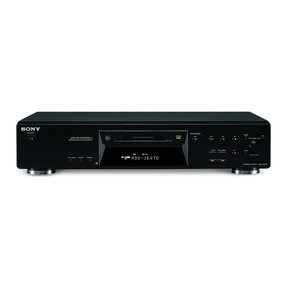
Sony MDS-JE470 - Md Player Service Manual
Minidisc deck
Hide thumbs
Also See for MDS-JE470 - Md Player:
- Operating instructions manual (48 pages) ,
- Limited warranty (1 page)
Table of Contents
Advertisement
SERVICE MANUAL
Ver 1.0 2001. 05
US and foreign patents licensed form Dolby Laboratories
Licensing Corporation.
System
Disc
Laser
Laser output
1)
This output is the value measured at a distance of
200 mm from the objective lens surface on the
Optical Pick-up Block with 7 mm aperture.
Laser diode
Revolutions (CLV)
Error correction
Sampling frequency
Coding
Modulation system
Number of channels
Frequency response
Signal-to-noise ratio
Wow and flutter
Sony Corporation
9-873-891-11
Home Audio Company
2001E0200-1
Shinagawa Tec Service Manual Production Group
© 2001.5
MDS-JE470
SPECIFICATIONS
MiniDisc digital audio
system
MiniDisc
Semiconductor laser
( λ = 780 nm) Emission
duration: continuous
MAX 44.6 µW
1)
Material: GaAlAs
400 rpm to 900 rpm
ACIRC (Advanced Cross
Interleave Reed Solomon
Code)
44.1 kHz
ATRAC (Adaptive
TRansform Acoustic
Coding)/ATRAC 3
EFM (Eight-to-Fourteen
Modulation)
2 stereo channels
5 to 20,000 Hz ±0.3 dB
Over 96 dB
during play
Below measurable limit
Canadian Model
Australian Model
Model Name Using Similar Mechanism
MD Mechanism Type
Optical Pick-up Type
I nputs
ANALOG IN
Jack type: phono
Impedance: 47 kilohms
Rated input: 500 mVrms
Minimum input:
125 mVrms
DIGITAL OPTICAL IN
Connector type: square
optical
Impedance: 660 nm
(optical wave length)
Outputs
ANALOG OUT
Jack type: phono
Rated output: 2 Vrms (at
50 kilohms)
Load impedance: over
10 kilohms
US Model
AEP Model
UK Model
E Model
MDS-S50
MDM-7A
KMS-260B/260E
— Continued on next page —
MINIDISC DECK
Advertisement
Table of Contents

Related Manuals for Sony MDS-JE470 - Md Player


Summary of Contents for Sony MDS-JE470 - Md Player
- Page 1 2 stereo channels 5 to 20,000 Hz ±0.3 dB Frequency response Signal-to-noise ratio Over 96 dB during play Wow and flutter Below measurable limit MINIDISC DECK Sony Corporation 9-873-891-11 Home Audio Company 2001E0200-1 Shinagawa Tec Service Manual Production Group © 2001.5...
- Page 2 E0001/ fingerprints, etc.), scratched, or the deck needs in order to operate. MEMORY NG substandard in quality. , Consult your nearest Sony dealer. , Replace the disc and repeat the There is a problem with the optical recording procedure. E0101/ pickup.
- Page 3 MDS-JE470 1. While pressing the lAMSL knob and x button, connect the power plug to the outlet, and release the lAMSL knob and x button. When the test mode is set, “[Check]” will be displayed. 2. Rotate the lAMSL knob and when “[Service]” is displayed, press the YES button. 3.
-
Page 4: Table Of Contents
MDS-JE470 Display History Mode for erasing the total spdl rp tm time spdl change These histories are based on the time of replacement of the spindle motor. If the spindle motor has been replaced, perform this procedure and erase the history. Procedure 1. -
Page 5: Servicing Notes
CRITIQUES POUR LA SÉCURITÉ DE FONCTIONNEMENT. NE COMPONENTS WITH SONY PARTS WHOSE PART NUMBERS REMPLACER CES COMPOSANTS QUE PAR DES PIÈSES SONY APPEAR AS SHOWN IN THIS MANUAL OR IN SUPPLEMENTS DONT LES NUMÉROS SONT DONNÉS DANS CE MANUEL OU PUBLISHED BY SONY. - Page 6 MDS-JE470 JIG FOR CHECKING BD BOARD WAVEFORM The special jig (J-2501-196-A) is useful for checking the waveform of the BD board. The names of terminals and the checking items to be performed are shown as follows. GND : Ground I+3V : For measuring IOP (Check the deterioration of the optical pick-up laser) IOP : For measuring IOP (Check the deterioration of the optical pick-up laser) : TRK error signal (Traverse adjustment) : Reference level for checking the signal...
- Page 7 MDS-JE470 Iop DATA RECORDING AND DISPLAY WHEN OPTICAL PICK-UP AND NON-VOLATILE MEMORY (IC195 OF BD BOARD) ARE REPLACED The Iop value labeled on the optical pick-up can be recorded in the non-volatile memory. By recording the value, it will eliminate the need to look at the value on the label of the optical pick-up.
- Page 8 MDS-JE470 OPTICAL PICK-UP BLOCK TYPE DISCRIMINATION There are two types of the optical pick-up block in this model. These are compatible except for the laser power. Check the type of the optical pick-up block before replacement. Ajdust following items after replacing the optical pick-up block. •...
- Page 9 MDS-JE470 CHECKS PRIOR TO PARTS REPLACEMENT AND ADJUSTMENTS Before performing repairs, perform the following checks to determine the faulty locations up to a certain extent. Details of the procedures are described in “5 Electrical Adjustments”. • 5-6-2. Laser power check (see page 28) •...
- Page 10 MDS-JE470 RETRY CAUSE DISPLAY MODE • In this test mode, the causes for retry of the unit during recording can be displayed on the fluorescent indicator tube. During playback, the “track mode” for obtaining track information will be set. This is useful for locating the faulty part of the unit. •...
- Page 11 MDS-JE470 Reading the Display: Convert the hexadecimal display into binary display. If more than two causes, they will be added. Example When 42 is displayed: Higher bit : 4 = 0100 t b6 Lower bit : 2 = 0010 t b1 In this case, the retry cause is combined of “CLV unlock”...
-
Page 12: General
MDS-JE470 SECTION 2 GENERAL This section is extracted from instruction manual. Parts Identification The items are arranged in alphabetical order. Refer to the pages indicated in parentheses ( ) for details. Main unit 0 qa STANDBY EJECT MENU/ MDLP TIMER GROUP REC OFF PLAY ON/OFF... -
Page 13: Disassembly
MDS-JE470 SECTION 3 DISASSEMBLY • This set can be disassembled in the order shown below. 3-1. DISASSEMBLY FLOW • Abbreviation : Singapore 3-2 UPPER CASE (408226) 3-5 PT BOARD 3-6 MECHANISM DECK 3-3 FRONT PANEL 3-4 MAIN BOARD VOL-SEL BOARD (SP model) SECTION (MDM-7A) SECTION 3-7 OVER LIGHT HEAD... -
Page 14: Upper Case (408226)
MDS-JE470 3-2. UPPER CASE (408226) 2 Case (408226) 1 Two screws (CASE 3TP2) 1 Screw (CASE 3TP2) 1 Two screws (CASE 3TP2) 3-3. FRONT PANEL SECTION 3 Connector (CN830) 5 Claw 2 Connector (CN390) 1 Wire (flat type) (17core) (CN3) 4 Two screws 5 Claw (+BVTP3x8) -
Page 15: Main Board
MDS-JE470 3-4. MAIN BOARD 6 Two screws (+BVTP3x8) 3 Connector (CN400) 2 Wire (flat type) (23core) (CN1) 1 Wire (flat type) (27core) (CN2) 7 MAIN board 4 Two screws (+BVTP3x8) 5 screw (+BVTP3x8) 3-5. PT BOARD, VOL-SEL BOARD (SP model) 3 Three screws (+PTTWH M3) 5 PT board... -
Page 16: Mechanism Deck Section (Mdm-7A)
MDS-JE470 3-6. MECHANISM DECK SECTION (MDM-7A) 3 Mechanism deck 2 Two step screws (+BVTTWH M3) 2 Two step screws (+BVTTWH M3) 1 Harness 3-7. OVER LIGHT HEAD (HR901), BD BOARD Note 1: If you disconnect the connector (CN104), you can remove the BD board without removing the over write head (HR901). -
Page 17: Holder Assy
MDS-JE470 3-8. HOLDER ASSY 2 Claw 6 Holder ASSY 4 Boss 4 Boss 1 Spring (holder), tension 3-9. LOADING MOTOR ASSY (M103) 1 Belt (loading) 2 Two screws (PWH1.7x2.5) 3 Motor ASSY, loading (M103) -
Page 18: Sled Motor Assy (M102), Slider
MDS-JE470 3-10. SLED MOTOR ASSY (M102), SLIDER 5 Remove the claw. Shift the slider in the arrow direction. 4 Slider (EJ) 8 Lever (head) 6 Slider 1 Two screws (BTP2X6) 2 Guide (L) 9 Two screws (PWH1.7X2.5) 7 Lever (CHG) 0 Motor ASSY, sled (M102) 3-11. -
Page 19: Spindle Moter Assy (M101)
MDS-JE470 3-12. SPINDLE MOTER ASSY (M101) 2 Spindle motor ASSY (M101) 1 Three screws (M1.7), tapping... -
Page 20: Test Mode
MDS-JE470 SECTION 4 TEST MODE 4-1. PRECAUTIONS FOR USE OF TEST MODE • As loading related operations will be performed regardless of the test mode operations being performed, be sure to check that the disc is stopped before setting and removing it. Even if the A EJECT button is pressed while the disc is rotating during continuous playback, continuous recording, etc., the disc will not stop rotating. - Page 21 MDS-JE470 4-5. SELECTING THE TEST MODE There are 26 types of test modes as shown below. The groups can be switched by rotating the l AMS L knob. After selecting the group to be used, press the YES button. After setting a certain group, rotating the l AMS L knob switches between these modes. Refer to “Group”...
- Page 22 MDS-JE470 4-5-1. Operating the Continuous Playback Mode 1. Entering the continuous playback mode 1 Set the disc in the unit. (Whichever recordable discs or discs for playback only are available.) 2 Rotate the l AMS L knob and display “CPLAY1 MODE”(C34). 3 Press the YES button to change the display to “CPLAY1 MID”.
- Page 23 MDS-JE470 4-6. FUNCTIONS OF OTHER BUTTONS Function Contents Sets continuous playback when pressed in the STOP state. When pressed during continuous playback, the tracking servo turns ON/OFF. Stops continuous playback and continuous recording. The sled moves to the outer circumference only when this is pressed. The sled moves to the inner circumference only when this is pressed.
- Page 24 MDS-JE470 4-8. MEANINGS OF OTHER DISPLAYS Contents Display When Lit When Off Servo ON Servo OFF Tracking servo OFF Tracking servo ON Recording mode ON Recording mode OFF SYNC CLV low speed mode CLV normal mode L.SYNC ABCD adjustment completed OVER Tracking offset cancel ON Tracking offset cancel OFF...
-
Page 25: Electrical Adjustments
MDS-JE470 SECTION 5 ELECTRICAL ADJUSTMENTS Note : 260B: KMS-260B 260E: KMS-260E 5-1. PARTS REPLACEMENT AND ADJUSTMENT If malfunctions caused by Optical pick-up such as sound skipping are suspected, follow the following check. Check before replacement Start 5-6-2. Laser Power Check (See page 28) 5-6-3. - Page 26 MDS-JE470 Adjustment flow • Abbreviation Start OP: Optical pick-up After turning off and then on the power, initialize the EEPROM Replace IC195 For details, refer to 4-11. WHEN MEMORY NG IS DISPLAYED (See page 24) 5-7. INITIAL SETTING OF ADJUSTMENT VALUE Replace OP or IO195 (See page 31) 5-9.
- Page 27 MDS-JE470 5-2. PRECAUTIONS FOR CHECKING LASER DIODE EMISSION To check the emission of the laser diode during adjustments, never view directly from the top as this may lose your eye-sight. 5-3. PRECAUTIONS FOR USE OF OPTICAL PICK- UP (KMS-260B/260E) As the laser diode in the optical pick-up is easily damaged by static electricity, solder the laser tap of the flexible board when using it.
- Page 28 MDS-JE470 5-5. USING THE CONTINUOUSLY RECORDED DISC Checking Procedure: 1. Set the laser power meter on the objective lens of the optical * This disc is used in focus bias adjustment and error rate check. pick-up. (When it cannot be set properly, press the m button The following describes how to create a continuous recording or M button to move the optical pick-up.) disc.
- Page 29 MDS-JE470 5-6-4. Auto Check 6. Observe the waveform of the oscilloscope, and check that the This test mode performs C-REC and C-PLAY automatically for specified value is satisfied. Do not rotate the AMS knob. mainly checking the characteristics of the optical pick-up. To (Read power traverse checking) perform this test mode, the laser power must first be checked.
- Page 30 MDS-JE470 16. Observe the waveform of the oscilloscope, and check that the 5-6-8. C PLAY Check specified value is satisfied. Do not rotate the l AMS L knob. MO Error Rate Check Checking Procedure : (Traverse Waveform) 1. Load a continuously recorded test disc (MDW-74/GA-1). (Refer to “5-5.
- Page 31 MDS-JE470 5-7. INITIAL SETTING OF ADJUSTMENT VALUE 5-9. TEMPERATURE COMPENSATION OFFSET ADJUTMENT Note: Save the temperature data at that time in the non-volatile memory Mode which sets the adjustment results recorded in the non-vola- as 25 ˚C reference data. tile memory to the initial setting value. However the results of the Note : temperature compensation offset adjustment will not change to the 1.
- Page 32 MDS-JE470 7. Then, rotate the l AMS L knob and display “LDPWR 5-12. TRAVERSE ADJUSTMENT CHECK”. Connection : 8. Press the YES button once and display “LD 0.9 mW $ ”. Oscilloscope Check that the reading of the laser power meter become the speci- fied value.
- Page 33 MDS-JE470 11. Rotate the l AMS L knob until the waveform of the 5-13. FOCUS BIAS ADJUSTMENT oscilloscope moves closer to the specified value. Adjusting Procedure : In this adjustment, waveform varies at intervals of approx. 2%. 1. Load a test disk (MDW-74/GA-1). Adjust the waveform so that the specified value is satisfied as 2.
- Page 34 MDS-JE470 5-14. ERROR RATE CHECK 5-16. AUTO GAIN CONTROL OUTPUT LEVEL 5-14-1. CD Error Rate Check ADJUSTMENT Checking Procedure : Be sure to perform this adjustment when the Optical pick-up is re- 1. Load a check disc (MD) TDYS-1. placed. 2.
- Page 35 MDS-JE470 5-17. ADJUSTING POINTS AND CONNECTING POINTS [BD BOARD] (SIDE A) CN101 D101 [BD BOARD] (SIDE B) IC101 CN105 IC102 NOTE IC151 IC190 IC195 1 27 CN103 CN102 NOTE:It is useful to use the jig. for checking the waveform. (Refer to Servicing Note on page 6.)
-
Page 36: Diagrams
MDS-JE470 SECTION 6 DIAGRAMS 6-1. CIRCUIT BOARDS LOCATION PT board VOL-SEL board (SP model) KEY-SW board MAIN board DISPLAY board BD board • Abbreviation : Singapore model... - Page 37 MDS-JE470 • WAVEFORMS THIS NOTE IS COMMON FOR PRINTED WIRING BOARDS AND SCHEMATIC DIAGRAMS. – BD Board – – MAIN Board – (In addition to this, the necessary note is printed in each block.) IC101 ek (RF) IC1 qd (XOUT) These are omitted.
-
Page 38: Bd Section
MDS-JE470 6-2. BLOCK DIAGRAMS – BD SECTION – DIGITAL SIGNAL PROCESSOR, EFM/ACIRC ENCODER/DECODER, SHOCK PROOF MEMORY CONTROLLER, ATRAC ENCODER/DECODER IC151 (1/2) IC151 (1/2) OVER WRITE EFMO ADDT ADDT HEAD DRIVE IC181 SAMPLING DATAI (Page39) , Q181, 182 HR901 FILI RATE SCTX XBCKI OVER WRITE HEAD... -
Page 39: Main Section
MDS-JE470 – MAIN SECTION – A/D, D/A CONVERTER IC500 • SIGNAL PATH J300 : PLAY (ANALOG OUT) : REC (ANALOG IN) AINL HIGH-PASS FILTER, LINE AMP ADDT SDTO SUB- ANALOG DIGITAL CONVERTER AINR TRACKTION IC310 ATTENUATOR BLOCK (Page38) AUDIO INTERFACE LOW-PASS AOUTL+ MIX AMP... -
Page 40: Printed Wiring Board - Bd Board
MDS-JE470 6-3. PRINTED WIRING BOARD – BD Board – • See page 36 for Circuit Board Location. There are a few cases that the part isn’t mounted in model is printed on diagram. OPTICAL PICK - UP BLOCK (KMS - 260B/260E) BD BOARD (SIDE B) BD BOARD... -
Page 41: Schematic Diagram - Bd Section (1/2)
MDS-JE470 6-4. SCHEMATIC DIAGRAM – BD SECTION (1/2) – • See page 37 for Waveforms. • See page 52 for IC Pin Functions. • See page 50 for IC Block Diagrams. BOARD (KMS - 260B/260E) (2/2) (Page 42) BOARD (2/2) (Page 42) BOARD (2/2) -
Page 42: Schematic Diagram - Bd Section (2/2)
MDS-JE470 6-5. SCHEMATIC DIAGRAM – BD SECTION (2/2) – • See page 37 for Waveforms. • See page 53 for IC Pin Functions. • See page 50 for IC Block Diagrams. BOARD (1/2) MAIN (Page 41) BOARD(1/2) (Page 43) BOARD (1/2) (Page 41) MAIN... -
Page 43: Schematic Diagram - Main Section (1/2)
MDS-JE470 6-6. SCHEMATIC DIAGRAM – MAIN SECTION (1/2) – • See page 37 for Waveforms. • See page 56 for IC Pin Functions. • See page 51 for IC Block Diagrams. -
Page 44: Schematic Diagram - Main Section (2/2)
MDS-JE470 6-7. SCHEMATIC DIAGRAM – MAIN SECTION (2/2) – • See page 51 for IC Block Diagrams. -
Page 45: Printed Wiring Board - Main Section
MDS-JE470 6-8. PRINTED WIRING BOARD – MAIN SECTION – • See page 36 for Circuit Board Location. There are a few cases that the part isn’t mounted in model is printed on diagram. • Semiconductor DISPLAY BOARD Location CN701 BD BOARD (Page46) CN102 Ref. -
Page 46: Printed Wiring Board - Display Section
MDS-JE470 6-9. PRINTED WIRING BOARD – DISPLAY SECTION – • See page 36 for Circuit Board Location. There are a few cases that the part isn’t mounted in model is printed on diagram. DISPLAY BOARD FLUORESCENT INDICATOR TUBE 3 2 1 1-681-736- (12) MAIN... -
Page 47: Schematic Diagram - Display Section
MDS-JE470 6-10. SCHEMATIC DIAGRAM – DISPLAY SECTION –... -
Page 48: Printed Wiring Board - Power Section
MDS-JE470 6-11. PRINTED WIRING BOARD – POWER SECTION – • See page 36 for Circuit Board Location. There are a few cases that the part isn’t mounted in model is printed on diagram. VOLTAGE SELECT VOL-SEL BOARD 115V 230V AC IN 1-681-738- (12) PT BOARD... -
Page 49: Schematic Diagram - Power Section
MDS-JE470 6-12. SCHEMATIC DIAGRAM – POWER SECTION –... -
Page 50: Ic Block Diagrams
MDS-JE470 6-13. IC BLOCK DIAGRAMS IC151 CXD2662R (BD BOARD) IC101 CXA2523AR (BD BOARD) 100 99 98 97 96 95 94 93 92 91 90 89 88 87 86 85 84 83 82 81 80 79 78 77 76 SPINDLE GENERATOR SERVO 75 TE MNT0... - Page 51 MDS-JE470 IC500 AK4524 (MAIN BOARD) VCOM AINR AOUTR+ AOUTR– CONVERTER CONVERTER AOUTL+ BLOCK BLOCK AOUTL– AINL VREF AGND DGND TEST CLOCK GENERATOR CLKO & DIVIDER XTALE 10 H.P.F. LRCK 11 D-ATT CONTROL AUDIO BICK 12 INTERFACE REGISTER SDTO 13 CCLK INTERFACE CONTROLLER D-ATT,...
-
Page 52: Ic Pin Functions
MDS-JE470 6-14. IC PIN FUNCTION DESCRIPTION • IC101 CXA2523AR RF Amplifier (BD BOARD) Pin No. Pin Name Description I-V converted RF signal I input I-V converted RF signal J input Middle point voltage (+1.5V) generation output 4 - 9 A to F Signal input from the optical pick-up detector Light amount monitor input Laser APC output... - Page 53 MDS-JE470 • IC151 CXD2662R Digital Signal Processor, Digital Servo Signal Processor (BD BOARD) Pin No. Pin Name Desription MNT0 (FOK) Not used (open) MNT1 (SHCK) Track jump detection signal output to the system control MNT2 (XBUSY) In the state of executire command signal output MNT3 (SLOC) Not used (open) SWDT...
- Page 54 MDS-JE470 Pin No. Pin Name Description Data input/output for DRAM 50, 51 D2, D3 MVCI I (S) Clock input from an external VCO (Fixed at “L”) ASYO Playback EFM duplex signal output ASYI I (A) Playback EFM comparator slice level input AVDD +3V power supply (Analog) BIAS...
- Page 55 MDS-JE470 Pin No. Pin Name Description Tracking servo drive PWM output (+) TFDR +3V power supply (Digital) DVDD Focus servo drive PWM output (+) FFDR Focus servo drive PWM output (–) FRDR 176.4 kHz clock signal output (X’tal) (Not used) Sled servo drive PWM output (–) SRDR Sled servo drive PWM output (+)
- Page 56 MDS-JE470 • IC1 M30803MG-107FP SYSTEM CONTROL (MAIN BOARD) Pin No. Pin Name Description FLDT Serial data signal output to the display driver. FLCK Serial clock signal output to the display driver. L: Active A1-IN A1 Control input. (Fixed at L) SIRCS Remote control input.
- Page 57 MDS-JE470 Pin No. Pin Name Description ADA. LATCH Latch signal output to the AK4524. L: Active Not used. (Fixed at L) L : DINT1/H : CLIP — Not used. (open) — Not used. PROTECT Recording-protection claw detection input from the protection detection switch. H: Protect Clock signal output to the EEP-ROM.
- Page 58 MDS-JE470 Pin No. Pin Name Description Strobe signal output to the power supply circuit. H: Power supply ON: L: standby BEEP SW — Not used. — Not used. FLCS Chip select signal output to the MSM9202 (IC760) 85, 86 D.VOL0,1 —...
-
Page 59: Exploded Views
MDS-JE470 SECTION 7 EXPLODED VIEWS NOTE: • -XX, -X mean standardized parts, so they may • Color indication of Appearance Parts have some differences from the original one. Example : The components identified by mark 0 or • Items marked “*” are not stocked since they KNOB, BALANCE (WHITE) (RED) dotted line with mark 0 are critical for safety. -
Page 60: Front Panel Section
MDS-JE470 7-2. FRONT PANEL SECTION 59 54 FL750 supplied Ref. No. Part No. Description Remarks Ref. No. Part No. Description Remarks X-4953-710-1 PANEL ASSY, FRONT...(BLACK) A-2007-911-A DISPLAY BOARD, COMPLETE (AEP,UK,HK,AUS) (AEP,UK,HK,SP,AUS) X-4953-711-1 PANEL ASSY, FRONT...(SILVER) (AEP,UK) A-2007-915-A DISPLAY BOARD, COMPLETE (SP) X-4953-712-1 PANEL ASSY, FRONT...(BLACK) (US,CND) 4-949-935-41 CUSHION (FL) 4-951-620-01 SCREW (2.6X8), +BVTP... -
Page 61: Mechanism Section-1 (Mdm-7A)
MDS-JE470 7-3. MECHANISM SECTION-1 (MDM-7A) Ref. No. Part No. Description Remarks Ref. No. Part No. Description Remarks 4-996-267-01 BASE (BU-D) 4-231-118-01 SPRING (HOLDER), TENSION 4-231-319-01 SCREW (2X6) CZN, +B (P) TRI 4-227-019-02 PLATE (HOLDER) ASSY, RETAINER 4-227-007-01 GEAR (SB) 4-227-013-01 SPRING (EJ), TENSION 4-227-025-01 BELT (LOADING) 4-226-995-01 SLIDER (EJ) 3-372-761-01 SCREW (M1.7), TAPPING... -
Page 62: Mechanism Section-2 (Mdm-7A)
MDS-JE470 7-4. MECHANISM SECTION-2 (MDM-7A) HR901 359 362 S102 M101 M102 not supplied M103 The components identified by Les composants identifiés par mark 0 or dotted line with mark une marque 0 sont critiques 0 are critical for safety. pour la sécurité. Replace only with part number Ne les remplacer que par une specified. -
Page 63: Electrical Parts List
MDS-JE470 SECTION 8 ELECTRICAL PARTS LIST Ref. No. Part No. Description Remarks Ref. No. Part No. Description Remarks NOTE: • Due to standardization, replacements in the • COILS When indicating parts by reference number, uH: µH parts list may be different from the parts please include the board name. - Page 64 MDS-JE470 Ref. No. Part No. Description Remarks Ref. No. Part No. Description Remarks IC190 8-759-460-72 IC BA033FP-E2 R116 1-216-839-11 METAL CHIP 1/16W IC195 8-759-640-41 IC BR24C08F-E2 R117 1-216-837-11 METAL CHIP 1/16W R118 1-218-855-11 METAL CHIP 2.2K 0.5% 1/16W <JUMPER RESISTOR> R119 1-218-863-11 METAL CHIP 4.7K...
- Page 65 MDS-JE470 MAIN KEY-SW DISPLAY Ref. No. Part No. Description Remarks Ref. No. Part No. Description Remarks A-2007-907-A DISPLAY BOARD, COMPLETE (US,CND) R781 1-249-401-11 CARBON 1/4W F A-2007-911-A DISPLAY BOARD, COMPLETE (AEP,UK,HK,AUS) R782 1-247-807-31 CARBON 1/4W A-2007-915-A DISPLAY BOARD, COMPLETE (SP) ************************* <SWITCH>...
- Page 66 MDS-JE470 MAIN Ref. No. Part No. Description Remarks Ref. No. Part No. Description Remarks 1-164-159-11 CERAMIC 0.1uF C520 1-126-934-11 ELECT 220uF 1-162-306-11 CERAMIC 0.01uF C522 1-164-159-11 CERAMIC 0.1uF 1-162-306-11 CERAMIC 0.01uF C523 1-104-665-11 ELECT 100uF 1-162-294-31 CERAMIC 0.001uF C524 1-164-159-11 CERAMIC 0.1uF C100 1-126-964-11 ELECT...
- Page 67 MDS-JE470 MAIN Ref. No. Part No. Description Remarks Ref. No. Part No. Description Remarks <FERRITE BEAD> 1-249-429-11 CARBON 1/4W 1-249-429-11 CARBON 1/4W FB460 1-414-093-11 FERRITE FB465 1-414-093-11 FERRITE 1-249-429-11 CARBON 1/4W R100 1-249-441-11 CARBON 100K 1/4W <IC> R111 1-249-435-11 CARBON 1/4W R112 1-249-431-11 CARBON...
- Page 68 MDS-JE470 VOL-SEL MAIN Ref. No. Part No. Description Remarks Ref. No. Part No. Description Remarks R513 1-249-401-11 CARBON 1/4W F 1-681-738-12 VOL-SEL BOARD (SP) R514 1-249-401-11 CARBON 1/4W F ************* R515 1-247-807-31 CARBON 1/4W R516 1-247-807-31 CARBON 1/4W <CONNECTOR> R517 1-247-807-31 CARBON 1/4W CN990...
- Page 69 MDS-JE470...
- Page 70 MDS-JE470 REVISION HISTORY Clicking the version allows you to jump to the revised page. Also, clicking the version at the upper right on the revised page allows you to jump to the next revised page. Ver. Date Description of Revision 2001.05...
Need help?
Do you have a question about the MDS-JE470 - Md Player and is the answer not in the manual?
Questions and answers