Table of Contents
Advertisement
SERVICE MANUAL
Ver. 1.4 2007.12
• SonicStage and the SonicStage logo are trademarks or registered trademarks of Sony
Corporation.
• OpenMG, ATRAC, ATRAC3, ATRAC3plus, ATRAC Advanced Lossless and their logos are
trademarks of Sony Corporation.
• "WALKMAN"and "WALKMAN" logo are registered trademarks of Sony Corporation.
is a trademark of Sony Corporation.
• Microsoft, Windows, Windows Vista and Windows Media are trademarks or registered
trademarks of Microsoft Corporation in the United States and/or other countries.
• Adobe and Adobe Reader are trademarks or registered trademarks of Adobe Systems
Incorporated in the United States and/or other countries.
• MPEG Layer-3 audio coding technology and patents licensed from Fraunhofer IIS and
Thomson.
• IBM and PC/AT are registered trademarks of International Business Machines Corporation.
• Macintosh is a trademark of Apple Inc.
• QuickTime is a trademark or registered trademark of Apple Inc. in the U.S. and/or other
countries.
• Pentium is a trademark or a registered trademark of Intel Corporation.
• This software is based in part on the work of the Independent JPEG Group.
• THIS PRODUCT IS LICENSED UNDER THE MPEG-4 VISUAL PATENT PORTFOLIO
LICENSE FOR THE PERSONAL AND NON-COMMERCIAL USE OF A CONSUMER FOR
(i) ENCODING VIDEO IN COMPLIANCE WITH THE MPEG-4 VISUAL STANDARD
("MPEG-4 VIDEO") AND/OR
(ii) DECODING MPEG-4 VIDEO THAT WAS ENCODED BY A CONSUMER ENGAGED
IN A PERSONAL AND NON-COMMERCIAL ACTIVITY AND/OR WAS OBTAINED
FROM A VIDEO PROVIDER LICENSED BY MPEG LA TO PROVIDE MPEG-4 VIDEO.
NO LICENSE IS GRANTED OR SHALL BE IMPLIED FOR ANY OTHER USE.
ADDITIONAL INFORMATION INCLUDING THAT RELATING TO PROMOTIONAL,
INTERNAL AND COMMERCIAL USES AND LICENSING MAY BE OBTAINED FROM
FROM MPEG LA, LLC. SEE HTTP://WWW.MPEGLA.COM
• THIS PRODUCT IS LICENSED UNDER THE AVC PATENT PORTFOLIO LICENSE FOR
THE PERSONAL AND NON-COMMERCIAL USE OF A CONSUMER TO
(i) ENCODE VIDEO IN COMPLIANCE WITH THE AVC STANDARD ("AVC VIDEO")
AND/OR
(ii) DECODE AVC VIDEO THAT WAS ENCODED BY A CONSUMER ENGAGED IN A
PERSONAL AND
NON-COMMERCIAL ACTIVITY AND/OR WAS OBTAINED FROM A VIDEO PROVIDER
LICENSED TO PROVIDE AVC VIDEO. NO LICENSE IS GRANTED OR SHALL BE
IMPLIED FOR ANY OTHER USE.
ADDITIONAL INFORMATION MAY BE OBTAINED FROM MPEG LA, L.L.C. SEE
HTTP://MPEGLA.COM
• US and foreign patents licensed from Dolby Laboratories.
• All other trademarks and registered trademarks are trademarks or registered trademarks of their
respective holders. In this manual,
TM
and
®
marks are not specified.
This product is protected by certain intellectual property rights of Microsoft Corporation.
Use or distribution of such technology outside of this product is prohibited without a license from
from Microsoft or an authorized Microsoft subsidiary.
Program ©2007 Sony Corporation
Documentation ©2007 Sony Corporation
Sony Corporation
9-887-631-05
Audio Business Group
2007L05-1
Published by Sony Techno Create Corporation
© 2007.12
NW-A805/A806/A808/
NWZ-A815/A816/A818
Photo: NW-A808
Supported file format
Music (NW-A805/A806/A808)
Codec
MP3
WMA*
ATRAC
ATRAC
Advanced
Lossless*
AAC*
The number of songsMax. 65,535
Music (NWZ-A815/A816/A818)
File format
MP3(MPEG1 Layer3) file format, ASF file format, MP4 file format, Wave-Riff file
format
File extension
File extension MP3 (.mp3), WMA (.wma), AAC-LC*
Codec
MP3
Linear PCM
Video
Video
File format
MP4 file format, "Memory Stick" video format
File extension
.mp4, .m4v
Codec
MP3
Audio
File size
Max. 2 GB
The number of files
Max. 1,000
US Model
NWZ-A815/A816/A818
Canadian Model
AEP Model
UK Model
Australian Model
New Zealand Model
Hong Kong Model
Singapore Model
NW-A805/A806/A808/NWZ-A815/A816/A818
Chinese Model
Tourist Model
NW-A805/A806/A808
SPECIFICATIONS
Bit rate: 32 to 320 kbps, variable bit rate-compliant (VBR)
Sampling frequency*
1
: 32, 44.1, 48 kHz
2
Bit rate: 32 to 192 kbps, variable bit rate-compliant (VBR)
Sampling frequency*
1
: 44.1 kHz
3
3
Bit rate: 48 to 352 kbps (66*
, 105*
, 132 kbps for ATRAC3)
Sampling frequency*
1
: 44.1 kHz
Bit rate: 64 to 352 kbps (132 kbps for ATRAC3 base layer)
Sampling frequency*
1
: 44.1 kHz
4
2
Bit rate: 16 to 320 kbps, variable bit rate-compliant (VBR)*
1
Sampling frequency*
: 8, 11.025, 12, 16, 22.05, 24, 32, 44.1, 48 kHz
1
(.mp4, .m4a, .3gp), Linear PCM
(.wav)
Bit rate: 32 to 320 kbps (Supports variable bit rate (VBR))
2
Sampling frequency*
: 32, 44.1, 48 kHz
2
WMA*
Bit rate: 32 to 192 kbps (Supports variable bit rate (VBR))
2
Sampling frequency*
: 44.1 kHz
2
AAC-LC*
Bit rate: 16 to 320 kbps (Supports variable bit rate (VBR))*
2
Sampling frequency*
: 8, 11.025, 12, 16, 22.05, 24, 32, 44.1, 48 kHz
Bit rate: 1,411 kbps
2
Sampling frequency*
: 44.1 kHz
MPEG-4
Profile: Simple Profile
(NW-A805/A806/A808)
Bit rate: Max. 2,500 kbps
AVC
Profile: Baseline Profile
(H.264/AVC)
Level: 1.2, 1.3
Bit rate: Max. 768 kbps
Frame rate: Max. 30 fps
Resolution: Max. QVGA (320 × 240)
AAC-LC
Channel number: Max. 2 channels
Sampling frequency: 24, 32, 44.1, 48 kHz
Bit rate: Max. 288 kbps per 1 channel
– Continued on next page –
DIGITAL MEDIA PLAYER
E Model
5
3
Advertisement
Table of Contents

Related Manuals for Sony NWZA816P - DIGITAL MEDIA PLAYER/MP3 PLAYER


Summary of Contents for Sony NWZA816P - DIGITAL MEDIA PLAYER/MP3 PLAYER
-
Page 1: Specifications
E Model Chinese Model Tourist Model NW-A805/A806/A808 Photo: NW-A808 • SonicStage and the SonicStage logo are trademarks or registered trademarks of Sony SPECIFICATIONS Corporation. Supported file format • OpenMG, ATRAC, ATRAC3, ATRAC3plus, ATRAC Advanced Lossless and their logos are trademarks of Sony Corporation. - Page 2 NW-A805/A806/A808/NWZ-A815/A816/A818 Ver. 1.2 Interface Photo* Headphone: Stereo mini-jack File format Compatible with DCF 2.0/Exif 2.21file format WM-PORT (multiple connecting terminal): 22 pins File extension .jpg Hi-Speed USB (USB 2.0 compliant) Codec JPEG (Baseline) Number of pixels: Max. 4,000 × 4,000 pixels (16,000,000 pixels) Operating temperature The number of files Max.
-
Page 3: Table Of Contents
NW-A805/A806/A808/NWZ-A815/A816/A818 Ver. 1.2 SECTION 1 SERVICING NOTES TABLE OF CONTENTS UNLEADED SOLDER Boards requiring use of unleaded solder are printed with the lead- SERVICING NOTES free mark (LF) indicating the solder contains no lead..........3 (Caution: Some printed circuit boards may not come printed with the lead free mark due to their particular size) GENERAL .............. - Page 4 NW-A805/A806/A808/NWZ-A815/A816/A818 Ver. 1.3 NOTE THE MAIN BOARD REPLACING When the MAIN board is replaced, format it according to the following. Formatting Memory (Format) You can format the built-in flash memory of the player. If the memory is formatted, all music, video and photo data, etc., will be erased.
- Page 5 NW-A805/A806/A808/NWZ-A815/A816/A818 Ver. 1.4 COLOR VARIATION COLOR Model Destination BLACK VIOLET WHITE PINK SILVER BLUE AEP, UK NW-A805 E, AUS, JE AEP, UK NW-A806 E, AUS, JE AEP, UK NW-A808 E, AUS, JE US (CircuitCity) NWZ-A815 CND, AEP, UK, NZ, HK, SP, AUS z (Note) US (BestBuy) US (CircuitCity)
-
Page 6: General
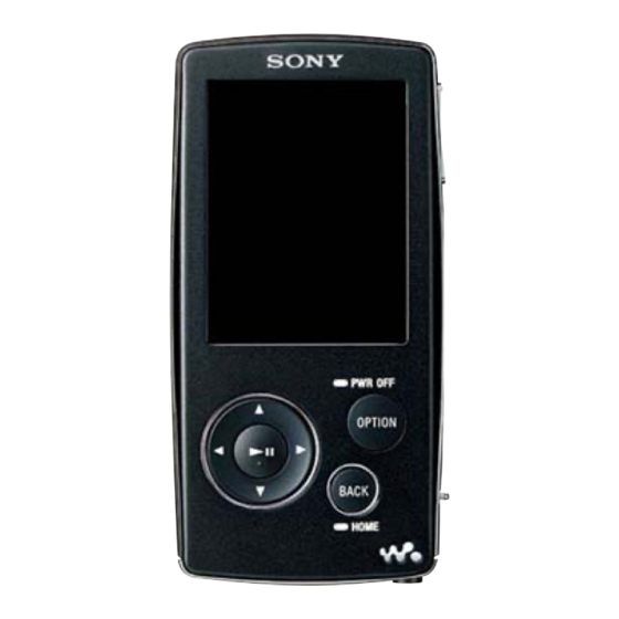
NW-A805/A806/A808/NWZ-A815/A816/A818 SECTION 2 This section is extracted from instruction manual. GENERAL Parts and Controls Front Rear 1 5-way button* 8 Strap hole 5 OPTION/PWR OFF button* Starts playback and enables Displays the Option menu. This is used to attach a strap (sold navigation of the player’s on-screen If you press and hold the OPTION/ separately). -
Page 7: Disassembly
NW-A805/A806/A808/NWZ-A815/A816/A818 Ver. 1.3 SECTION 3 DISASSEMBLY • This set can be disassembled in the order shown below. 3-1. DISASSEMBLY FLOW 3-2. REAR CABINET ASSY (Page 7) 3-3. MAIN BOARD (Page 8) 3-4. HOLDER CONNECTOR (Page 8) 3-5. NAND BOARD, 3-6. NOTE WHEN INSTALLING THE SVX SWITCH FLEXIBLE (PWB ASSY) SVX SWITCH FLEXIBLE (PWB ASSY) (Page 9) (Page 9) -
Page 8: Main Board
NW-A805/A806/A808/NWZ-A815/A816/A818 3-3. MAIN BOARD 9 insulating sheet (main) 1 cushion (connector) q; spacer (PWB) 2 sheet (harness) 6 screw (M1.4) qa spacer (IC) qg MAIN board 4 battery assy connector (CN901) 3 LCD flexible board qf spacer (SRAM) (CN801) 8 connector (CN601) qs Remove two solders. -
Page 9: Nand Board, Svx Switch Flexible (Pwb Assy)
NW-A805/A806/A808/NWZ-A815/A816/A818 Ver. 1.4 3-5. NAND BOARD, SVX SWITCH FLEXIBLE (PWB ASSY) 9 sheet (NAND) (NW-A805/A806/ NWZ-A815/A816 only) 3 two screws (M1.4) q; spacer (NAND) qa NAND board 6 Remove three solders. 5 Lift up the NAND board. 4 Turn up the LCD flexible board. 2 Lift up the SVX swtch flexible (PWB assy). -
Page 10: Front Button
NW-A805/A806/A808/NWZ-A815/A816/A818 3-7. FRONT BUTTON 2 front button 1 Turn up the LCD flexible board. – rear view – 3-8. SVX LCD ASSY (LCD801), BATTERY ASSY 1 screw (B1.4) q; spacer (rear) 4 adhesive (LCD) Note: Adhesive (LCD) cannot re-used. Please replace to brand-new part ones adhesive (LCD) is removed. -
Page 11: Front Cabinet Assy
NW-A805/A806/A808/NWZ-A815/A816/A818 3-9. FRONT CABINET ASSY Note: NAND gasket cannot re-used. Note: The VOL button should be oriented Please replace to brand-new part as shown in the figure when it is installed. ones NAND gasket is removed. VOL button 3 NAND gasket 1 VOL button 4 conductive sheet (jack) rear cabinet assy... -
Page 12: Test Mode
NW-A805/A806/A808/NWZ-A815/A816/A818 SECTION 4 TEST MODE 4-1-1. Power supply voltage check Note: Information on the test mode must correspond in enough securi- This mode is used in case power supply voltage in the state where ty. When the leakage has been revealed by any chance, the source of information is specified. - Page 13 NW-A805/A806/A808/NWZ-A815/A816/A818 4-1-3. Standby current check 4-1-5. Battery voltage check This mode is used in case standby current is checked. This mode is used in case battery voltage is checked. Checking method: Checking method: 1. Enter the test mode. 1. Enter the test mode. 2.
- Page 14 NW-A805/A806/A808/NWZ-A815/A816/A818 4-2-1. Output check 4-2-3. Frequency characteristic 1 check “1 kHz 0 dBs L-ch/R-ch VOLUME: 25” audio signal is outputted. “20 Hz 0 dBs L-ch/R-ch VOLUME: 25” audio signal is outputted. Checking method: Checking method: 1. Enter the test mode. 1.
- Page 15 NW-A805/A806/A808/NWZ-A815/A816/A818 4-2-5. CH separation (L-ch) check 4-2-7. Maximum output check “1 kHz 0 dBs L-ch VOLUME: 25” audio signal is outputted. “1 kHz 0 dBs L-ch/R-ch VOLUME: 30” (Headphone output when AVLS operates: “1 kHz 0 dBs L-ch/R-ch VOLUME: 13”) audio sig- Checking method: nal is outputted.
- Page 16 NW-A805/A806/A808/NWZ-A815/A816/A818 4-4. Other 4-2-9. Sound pressure regulation level check “1 kHz 0 dBs L-ch/R-ch VOLUME: 30” audio signal is outputted. liquid crystal display Checking method: MPTAPP MENU 1. Enter the test mode. POWER 2. Press the key to select the “AUDIO”, and press the AUDIO key to enter the minor item.
- Page 17 NW-A805/A806/A808/NWZ-A815/A816/A818 4-4-2. Key check 4-4-6. Firmware version check 4-4-8. NAND capacity check The operation of the key is confirmed. The firmware version is displayed. (since firmware version 1.00.20) Capacity of NAND flash memory, present bud block, maximum Checking method: Checking method: bud block, and vender ID are displayed.
-
Page 18: Diagrams
NW-A805/A806/A808/NWZ-A815/A816/A818 SECTION 5 DIAGRAMS 5-1. BLOCK DIAGRAM SYSTEM CONTROLLER, POWER CONTROL, LCD DRIVER, NAND FLASH INTERFACE, HEADPHONE/LINE CONTROLLER MS INTERFACE, SD-RAM INTERFACE SELECTOR CN851 (1/2) IC501 IC601 IC303 (WM-PORT) J301 A/D CONVERTER, (HEADPHONE) D/A CONVERTER CD0 – CD15 USB DATA0 – USB DATA15 AB0_D0 –... - Page 19 NW-A805/A806/A808/NWZ-A815/A816/A818 Ver. 1.2 • Note for Printed Wiring Boards and Schematic Diagrams Note on Printed Wiring Board: Note on Schematic Diagram: • Y : parts extracted from the conductor side. • All capacitors are in µF unless otherwise noted. (p: pF) •...
-
Page 20: Printed Wiring Boards - Main Section (1/2)
NW-A805/A806/A808/NWZ-A815/A816/A818 • Semiconductor 5-2. PRINTED WIRING BOARDS – MAIN Section (1/2) – : Uses unleaded solder. Location Ref. No. Location IC501 IC502 IC503 IC504 IC505 IC506 IC507 IC508 IC509 IC601 MAIN BOARD (SIDE A) IC701 C613 C697 C650 C660 C671 C674 C677 C655... -
Page 21: Printed Wiring Boards - Main Section (2/2)
NW-A805/A806/A808/NWZ-A815/A816/A818 Ver. 1.2 • Semiconductor 5-3. PRINTED WIRING BOARDS – MAIN Section (2/2) – : Uses unleaded solder. Location Ref. No. Location D101 D201 IC301 IC302 IC303 IC602 IC802 IC803 IC901 MAIN BOARD (SIDE B) CL906 Q301 Q302 CL628 CL624 CL635 TH901 CL805... -
Page 22: Schematic Diagram - Main Section (1/6)
NW-A805/A806/A808/NWZ-A815/A816/A818 Ver. 1.2 • See page 28 for IC Block Diagrams. • See page 30 for IC Pin Function Description. 5-4. SCHEMATIC DIAGRAM – MAIN Section (1/6) – MAIN BOARD (1/6) R302 VDD_HP CRD_LINEOUT HP_XMUTE R102 22k R306 LINE_IN_L LINE_IN_R R202 R204 Q304... -
Page 23: Schematic Diagram - Main Section (2/6)
NW-A805/A806/A808/NWZ-A815/A816/A818 Ver. 1.1 • See page 28 for IC Block Diagrams. 5-5. SCHEMATIC DIAGRAM – MAIN Section (2/6) – MAIN BOARD (2/6) VDD_GP1 USB_INT R510 AB0_XDRQ R509 R520 100k IC B/D IC508 C516 TC7SG04AFS IC509 LEVEL SHIFT IC B/D IC509 IC506 C517 SN74AVC1T45YZPR... -
Page 24: Schematic Diagram - Main Section (3/6)
NW-A805/A806/A808/NWZ-A815/A816/A818 Ver. 1.1 • See page 28 for IC Block Diagrams. • See page 30 for IC Pin Function Description. 5-6. SCHEMATIC DIAGRAM – MAIN Section (3/6) – MAIN BOARD (3/6) VDD_GP1 VDD_GP1 CHG_PEN2 CHG_PEN2 CHG_XCHGEN CHG_XCHGEN VDD_LOG USB_SUSPEND VDD_LOG CL613 CL614 USB_SUSPEND... -
Page 25: Schematic Diagram - Main Section (4/6)
NW-A805/A806/A808/NWZ-A815/A816/A818 5-7. SCHEMATIC DIAGRAM – MAIN Section (4/6) – MAIN BOARD (4/6) VDD_ECO SDR_DQM0 SDR_DQM0 SDR_DQM1 SDR_DQM1 SDR_DQM2 SDR_DQM2 SDR_DQM3 SDR_DQM3 SDR_XWR SDR_XWR SDR_CKE0 SDR_CKE0 SDR_XCS0 SDR_XCS0 SDR_XRAS SDR_XRAS R701 C702 SDR_XCAS 100p SDR_XCAS C853 R857 100p SDR_BA1 470k CN851 SDR_BA1 SDR_BA0 (WM-PORT) -
Page 26: Schematic Diagram - Main Section (5/6)
NW-A805/A806/A808/NWZ-A815/A816/A818 • See page 28 for IC Block Diagrams. • See page 30 for IC Pin Function Description. 5-8. SCHEMATIC DIAGRAM – MAIN Section (5/6) – MAIN BOARD (5/6) R811 CN801 470k LED_- C811 LED_- LCD_PXCLK LCD_PXCLK LED_+ C812 LCD_VSYNC LCD_VSYNC LED_+ LCD_HSYNC... -
Page 27: Schematic Diagram - Main Section (6/6)
NW-A805/A806/A808/NWZ-A815/A816/A818 • See page 28 for IC Block Diagrams. 5-9. SCHEMATIC DIAGRAM – MAIN Section (6/6) – R902 MAIN BOARD (6/6) VDD_UNREG MAIN BOARD DGND IC903 IC B/D (2/6) (Page 23) DC/DC CONVERTER L901 µ IC903 MAX1557ETB VDD_DDCOUT20 C912 C921 C911 PGND 0.001... - Page 28 NW-A805/A806/A808/NWZ-A815/A816/A818 • IC Block Diagrams IC504 TK63718HCL-G IC505, 506 TC7WG74FC – MAIN Board – IC301 XC6401FF58DR IC303 MAX4764ETB+TG069 THERMAL & OVER CURRENT PROTECTION ON / OFF CONTROL REGULATOR VOLTAGE ON / OFF VCONT COM2 CONTROL XCLR REFERENCE REGULATOR 2 VOUT2 COM1 VOLTAGE REFERENCE...
- Page 29 NW-A805/A806/A808/NWZ-A815/A816/A818 IC901 MAX8677AETG 21 20 /DONE CURRENT-LIMITED VOLTAGE REGULATOR LITHIUM BATTERY INPUT CHARGER SYSTEM VOLTAGE LOAD SWITCH MONITOR /CEN TSET INPUT LIMITER & CHARGER THERMAL PEN1 REGULATION CURRENT PEN2 SETTING USUSS 10 11 12 IC903 MAX1557ETB 0.675V OUTPUT BIAS VOLTAGE CURRENT-LIMIT SELECTOR CURRENT...
- Page 30 NW-A805/A806/A808/NWZ-A815/A816/A818 • IC Pin Function Description MAIN BOARD IC302 CS42L51-CNZR (A/D CONVERTER, D/A CONVERTER) Pin No. Pin Name Description LRCK L/R sampling clock signal input/output with the system controller I2C mode : Serial date input/output with the system controller SDA/CDIN SPI mode : Serial date input from the system controller SCL/CCLK Serial data transfer clock signal input from the system controller...
- Page 31 NW-A805/A806/A808/NWZ-A815/A816/A818 MAIN BOARD IC601 MC-10051F1-FAE-A (SYSTEM CONTROLLER, POWER CONTROL, LCD DRIVER, NAND FLASH INTERFACE, MS INTERFACE, SD-RAM INTERFACE) Pin No. Pin Name Description A1 to A3 Not used NAND_WEZ Write enable signal output to the NAND flash memory IO_B Not used A6 to A10 Not used A11 to...
- Page 32 NW-A805/A806/A808/NWZ-A815/A816/A818 Pin No. Pin Name Description Not used SWADP Not used CAPVBDL Not used VCCVBAT Power supply terminal (battery power supply) Not used IO_A Not used AB0_A5 Address signal output to the USB controller Not used C21 to C24 AB0_D1 Serial date input/output with the USB controller Not used IDPULLUP...
- Page 33 NW-A805/A806/A808/NWZ-A815/A816/A818 Pin No. Pin Name Description FLASHCLK Flash clock output to the D flip-flop AB0_A7 Address signal output to the USB controller E21 to E23 Not used AB0_XDRQ DMA request signal input from the USB controller AB0_D4 Serial date input/output with the USB controller Not used DGND Ground terminal...
- Page 34 NW-A805/A806/A808/NWZ-A815/A816/A818 Pin No. Pin Name Description SDR_DATA28, K4, K5 Serial data input/output with the 256Mbit SD-RAM SDR_DATA26 NAND_RBZ3 Read/busy signal outoput to the NAND flash memory NAND_DA6 Serial date input/output with the NAND flash memory K10 to Ground terminal Not used LCD_HSYNC Horizontal sync signal output to the level shift Not used...
- Page 35 NW-A805/A806/A808/NWZ-A815/A816/A818 Pin No. Pin Name Description LCD_PXCLK Clock signal output to the level shift Not used P25, P26 IO_A Not used SDR_DATA0 Serial data input/output with the 256Mbit SD-RAM SDR_DQM3 to R2 to R4 Write mask signal output to the 256Mbit SD-RAM SDR_DQM1 SDR_WEZ Write enable signal output to the 256Mbit SD-RAM...
- Page 36 NW-A805/A806/A808/NWZ-A815/A816/A818 Pin No. Pin Name Description C_TCK Clock signal input terminal for JTAG Not used VPLL Power supply voltage output terminal Main system clock input terminal (11.2896MHz) V1 to V3 IO_A Not used V4, V5, SDR_A6, SDR_A5, Address signal output to the 256Mbit SD-RAM SDR_A7 Ground terminal CHG_XCHGEN...
- Page 37 NW-A805/A806/A808/NWZ-A815/A816/A818 Pin No. Pin Name Description AA25 VANAIN Power supply voltage input terminal AA26 VANA Power supply voltage output terminal VDD_L0 Power supply terminal XUSB_OK USB OK signal input from the charge control CRD_DET Wake up signal input from the WM-port CHG_XFLT Charge signal showing that the drive is in fault status is input SDR_BA0...
- Page 38 NW-A805/A806/A808/NWZ-A815/A816/A818 Pin No. Pin Name Description AC25 IO_C Not used AC26 OSCOUT Sub system clock output terminal (32.768kHz) Not used AD2, AD3 BDID1, BDID0 Not used XHOLD_KEY Key hold on/off signal input from the hold switch KEY_WAKE Wake up control signal input terminal Not used I2C mode : Address signal output to the D/A converter SPI0_CSZ2...
- Page 39 NW-A805/A806/A808/NWZ-A815/A816/A818 Pin No. Pin Name Description AE24 VGP45IN Power supply voltage input terminal AE25, AE26, AF1 Not used to AF3 DD2VFB2 Power supply voltage feedback terminal DD2INB1, AF5, AF6 Power supply voltage input terminal DD2INB2 DD2LX3, AF7 to DD2LX1, Power supply voltage output terminal DD2LX2 AF10, DD2GNDB1,...
- Page 40 NW-A805/A806/A808/NWZ-A815/A816/A818 MAIN BOARD IC803 XC2C64A-7CPG56C-01 (LEVEL SHIFT) Pin No. Pin Name Description R3_OUT to A1 to A4 Video signal (R) output to the liquid crystal display R0_OUT G5_OUT Video signal (G) output to the liquid crystal display Data output terminal for JTAG Not used G2_OUT, A7, A8 Video signal (G) output to the liquid crystal display...
-
Page 41: Exploded Views
NW-A805/A806/A808/NWZ-A815/A816/A818 Ver. 1.2 SECTION 6 EXPLODED VIEWS NOTE: Abbreviation -XX and -X mean standardized parts, so they Items marked “*” are not stocked since they AUS : Australian model may have some difference from the original are seldom required for routine service. Some : Chinese model one. -
Page 42: Rear Cabinet Section (Nwz-A815/A816/A818)
NW-A805/A806/A808/NWZ-A815/A816/A818 Ver. 1.3 6-2. REAR CABINET SECTION (NWZ-A815/A816/A818) (BLACK, SILVER, VIOLET, BLUE models only) not supplied MAIN board, NAND board section Note: Blue color type of NWZ-A816 US model is using parts of violet color type. Ref. No. Part No. Description Remark Ref. -
Page 43: Main Board, Nand Board Section (Nw-A805/A806/A808)
NW-A805/A806/A808/NWZ-A815/A816/A818 Ver. 1.2 6-3. MAIN BOARD, NAND BOARD SECTION (NW-A805/A806/A808) Note: The illustration sees the set from the rear. not supplied supplied not supplied (NW-A805/A806) front cabinet section Note: When the MAIN board is replaced, format it according to the “NOTE OF MAIN BOARD REPLACING”... -
Page 44: Main Board, Nand Board Section (Nwz-A815/A816/A818)
NW-A805/A806/A808/NWZ-A815/A816/A818 Ver. 1.3 6-4. MAIN BOARD, NAND BOARD SECTION (NWZ-A815/A816/A818) Note: The illustration sees the set from the rear. not supplied supplied not supplied (NWZ-A815/A816) front cabinet section Note: When the MAIN board is replaced, format it according to the “NOTE OF MAIN BOARD REPLACING”... -
Page 45: Front Cabinet Section
NW-A805/A806/A808/NWZ-A815/A816/A818 Ver. 1.4 6-5. FRONT CABINET SECTION Note: The illustration sees the set from the rear. LCD801 not supplied not supplied Note: Blue color type of NWZ-A816 US model is using parts of violet color type. Ref. No. Part No. Description Remark Ref. -
Page 46: Electrical Parts List
NW-A805/A806/A808/NWZ-A815/A816/A818 Ver. 1.2 SECTION 7 MAIN ELECTRICAL PARTS LIST NOTE: Abbreviation Due to standardization, replacements in the Items marked “*” are not stocked since they AUS : Australian model parts list may be different from the parts are seldom required for routine service. : Chinese model specified in the diagrams or the components Some delay should be anticipated when... - Page 47 NW-A805/A806/A808/NWZ-A815/A816/A818 MAIN Ref. No. Part No. Description Remark Ref. No. Part No. Description Remark C633 1-112-716-11 CERAMIC CHIP 0.1uF 6.3V C703 1-112-716-11 CERAMIC CHIP 0.1uF 6.3V C634 1-112-716-11 CERAMIC CHIP 0.1uF 6.3V C638 1-112-717-91 CERAMIC CHIP 6.3V C704 1-128-622-91 CERAMIC CHIP 100PF C640 1-112-717-91 CERAMIC CHIP...
- Page 48 NW-A805/A806/A808/NWZ-A815/A816/A818 Ver. 1.2 MAIN Ref. No. Part No. Description Remark Ref. No. Part No. Description Remark FB803 1-481-258-21 SMD EMI FERRITE R106 1-218-949-11 RES-CHIP 1/16W FB804 1-481-258-21 SMD EMI FERRITE R107 1-208-455-11 RES-CHIP 1/16W FB805 1-481-258-21 SMD EMI FERRITE (EXCEPT FR) FB806 1-481-258-21 SMD EMI FERRITE FB807...
- Page 49 NW-A805/A806/A808/NWZ-A815/A816/A818 MAIN Ref. No. Part No. Description Remark Ref. No. Part No. Description Remark R611 1-218-990-81 SHORT CHIP R816 1-218-990-81 SHORT CHIP R615 1-218-953-11 RES-CHIP 1/16W R851 1-218-953-11 RES-CHIP 1/16W R616 1-245-684-21 RES-CHIP 0.22 1/8W R617 1-245-684-21 RES-CHIP 0.22 1/8W R853 1-218-953-11 RES-CHIP 1/16W...
- Page 50 NW-A805/A806/A808/NWZ-A815/A816/A818 Ver. 1.4 NAND Ref. No. Part No. Description Remark Ref. No. Part No. Description Remark X-2177-781-1 NAND BOARD, COMPLETE (2GB) (for SERVICE) MISCELLANEOUS (NW-A805: CND) ************** X-2177-782-1 NAND BOARD, COMPLETE (4GB) (for SERVICE) (NW-A806: CND) X-2177-801-1 FLEXIBLE (PWB ASSY), SVX SWITCH X-2177-783-1 NAND BOARD, COMPLETE (8GB) (for SERVICE) X-2177-657-1 BATTERY (A) ASSY (for NW-A805/A806/A808) (NW-A808: CND)
- Page 51 NW-A805/A806/A808/NWZ-A815/A816/A818 Ver. 1.4 Ref. No. Part No. Description Remark Ref. No. Part No. Description Remark 3-270-643-32 MANUAL (QSG), INSTRUCTION X-2179-904-2 SOFT ASSY (BB), APPLICATION (Quick Start Guide) (GERMAN) (CD-ROM: MP3 Conversion Tool, (NWZ-A815: CND, AEP, UK, NZ, HK, SP, AUS/ Windows Media Player 11, A816: CND, AEP, UK, NZ, HK, SP, AUS/ Operation Guide (PDF file)) (for BestBuy)
-
Page 52: Revision History
NW-A805/A806/A808/NWZ-A815/A816/A818 REVISION HISTORY Clicking the version allows you to jump to the revised page. Also, clicking the version at the top of the revised page allows you to jump to the next revised page. Ver. Date Description of Revision 2007.04 2007.06 Addition of black color type to E, Australian and Tourist models (NW-A806)
Need help?
Do you have a question about the NWZA816P - DIGITAL MEDIA PLAYER/MP3 PLAYER and is the answer not in the manual?
Questions and answers