Table of Contents
Advertisement
Quick Links
Advertisement
Table of Contents

Related Manuals for Clevo L141PU


Summarization of Contents
Preface
Notice
Describes the company's rights to revise, liability, reproduction policy, and user backups.
Trademarks
Lists registered trademarks like Intel
and Microsoft
Windows.
About this Manual
Explains the manual's purpose, target audience, and content structure for servicing the notebook.
IMPORTANT SAFETY INSTRUCTIONS
Lists general safety precautions to reduce risk of fire, electric shock, and injury when using electrical equipment.
FCC Statement
Details compliance with Part 15 of FCC Rules, including conditions for operation and interference.
Instructions for Care and Operation
Provides guidelines on preventing damage from dropping, overheating, liquids, and proper shutdown procedures.
Power Safety
Discusses power adapter requirements, grounding, handling power cords, and battery safety.
Battery Precautions
Warns about battery usage, damage, repair, handling, and keeping children away from batteries.
Battery Guidelines
Covers guidelines for storing batteries for extended periods and checking stored batteries.
Battery Disposal
Explains the recyclability of batteries and legal disposal requirements according to local laws.
Powering the Computer On
Explains the steps for powering on the notebook, including connecting the AC/DC adapter.
System Startup
Details the initial setup procedures: removing packing, attaching peripherals, and connecting power.
Shut Down
Recommends shutting down the computer via the Windows command to prevent system problems.
Introduction
Overview
Describes the manual's scope, target audience, and related information sources for the notebook.
Specifications
Details processor options, BIOS, memory, LCD, storage, video adapter, audio, and security features.
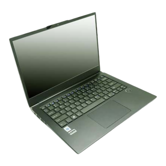
External Locator - Top View with LCD Panel Open
Identifies components visible on the top view of the laptop when the LCD panel is open.
External Locator - Front & Right Side Views
Identifies components on the front and right side views of the laptop, including ports and buttons.
External Locator - Left Side & Rear View
Identifies components on the left side and rear views of the laptop, including ports and speakers.
External Locator - Bottom View
Identifies components on the bottom view of the laptop, including vents and speakers.
Mainboard Overview - Top (Key Parts)
Identifies key components on the top side of the mainboard, such as the KBC-ITE IT5570.
Mainboard Overview - Bottom (Key Parts)
Identifies key components on the bottom side of the mainboard, including CPU and memory slots.
Mainboard Overview - Top (Connectors)
Identifies connectors on the top side of the mainboard, such as DC-In, HDMI, and USB ports.
Mainboard Overview - Bottom (Connectors)
Identifies connectors on the bottom side of the mainboard, such as speaker, fan, and battery connectors.
Disassembly
Overview
Explains the chapter's purpose: step-by-step disassembly instructions and margin box notations for procedures.
Maintenance Tools
Lists recommended tools for safely performing removal and replacement jobs on the notebook PC.
Connections
Describes four types of internal computer connectors and provides instructions on how to disconnect them.
Maintenance Precautions
Safety advice to avoid personal injury or damage during disassembly, including static discharge and corrosion.
Cleaning
Provides instructions for cleaning the computer case using a soft, clean cloth and avoiding harsh cleaners.
Disassembly Steps
Lists the sequential steps for disassembling components like battery, memory, WLAN, 4G, SSD, CCD, and LCD.
Removing the Battery
Step-by-step procedure for removing the notebook battery, including screw removal and cable disconnection.
Removing the Battery (Battery-2 Removal Procedure)
Alternative step-by-step procedure for removing the notebook battery, referencing Figure 1a-d.
Removing the System Memory (RAM)
Procedure for removing and upgrading DDR4 SO-DIMM memory modules using release latches.
Removing the Wireless LAN Module
Step-by-step guide to remove and replace the Wireless LAN module, including cable disconnection and screw removal.
Wireless LAN, and Combo Module Cables
Details color coding for WLAN, BT, 3G, and LTE module antenna cables for identification.
Removing the 4G Module
Procedure for removing and replacing the 4G module, involving cable disconnection and screw removal.
Removing the M.2 SSD Module (M.2 SSD1 Removal Procedure)
Step-by-step guide to remove the M.2 SSD1 module from the mainboard after screw removal.
Removing the M.2 SSD Module (M.2 SSD2 Removal Procedure)
Step-by-step guide to remove the M.2 SSD2 module from the mainboard after screw removal.
Removing the CCD
Procedure for removing the CCD module, including LCD front panel removal and cable disconnection.
Removing the LCD
Detailed steps for removing the LCD panel, including mylar removal, cable disconnection, and lifting.
Part Lists
Part Lists
Introduction to the appendix that breaks down notebook construction into illustrations and part numbers.
Part List Illustration Location
Table indicating where to find illustrations for different parts: Top, Bottom, LCD, and Mainboard.
Top
Illustration and part list for the top assembly, including case, keyboard, speakers, and battery tape.
Bottom
Illustration and part list for the bottom assembly, including bottom case, screws, and product labels.
LCD
Illustration and part list for the LCD assembly, including panel, front cover, camera, and microphone.
MB
Illustration and part list for the mainboard assembly, including CPU, SSD, heatsink, and battery.
Schematic Diagrams
Schematic Diagrams
Introduction to Appendix B, listing circuit diagrams for the notebook's PCB components and modules.
System Block Diagram
High-level diagram showing the interconnection of major components like CPU, memory, and I/O interfaces.
Processor 1/13
Detailed pinout and connections for Processor 1/13, related to memory (DQ, CLK, BA, A) and power.
Processor 2/13
Detailed pinout and connections for Processor 2/13, related to memory (DQ, CLK, BA, A) and power.
Processor 3/13
Detailed pinout and connections for Processor 3/13, related to display (eDP, HDMI) and I/O interfaces.
Processor 4/13
Detailed pinout and connections for Processor 4/13, related to I2C, ISH, AUDIO, and CNVI interfaces.
Processor 5/13
Detailed pinout and connections for Processor 5/13, related to PCIe, CLKREQ, XTAL, and SATA interfaces.
Processor 6/13
Detailed pinout and connections for Processor 6/13, related to PCIe, USB3, and USB2 interfaces.
Processor 7/13
Detailed pinout and connections for Processor 7/13, related to SPI, ESPI, THC, MLINK, SMBUS interfaces.
Processor 8/13
Detailed pinout and connections for Processor 8/13, related to CSI, CNV, RSVD, and M.2 interfaces.
Processor 9/13
Detailed pinout and connections for Processor 9/13, related to CPU JTAG, PCH JTAG, and MISC interfaces.
Processor 10/13
Detailed pinout and connections for Processor 10/13, related to SYSTEM POWER MANAGEMENT functions.
Processor 11/13
Detailed pinout and connections for Processor 11/13, related to CPU POWER stages (VCORE, VCCGT).
Processor 12/13
Detailed pinout and connections for Processor 12/13, related to PCH POWER stages (VCCIN, 1.8VA).
Processor 13/13
Detailed pinout and connections for Processor 13/13, showing GND pins and reserved signals.
DDR4 CH0-1
Schematic for DDR4 Channel 0, DIMM 1, showing memory pin connections and termination.
DDR4 CH0-2
Schematic for DDR4 Channel 0, DIMM 2, showing memory pin connections and termination.
DDR4 Terminations
Schematic showing termination resistors for DDR4 memory signals like CLK, DQ, and BA lines.
DDR4 Decaps
Schematic showing decoupling capacitors for DDR4 memory interfaces (VDDQ, VPP, VTT).
DDR4 SO-DIMM_1
Detailed schematic of DDR4 SO-DIMM connector 1 pinout and connections to the CPU.
HDMI
Schematic diagram for the HDMI port, including TMDS signals, DDC, CEC, and HPD.
Panel / 3.3VA
Schematic for the panel power and backlight control, including eDP connector pinout.
Retimer
Schematic for the Retimer IC, showing TBT ports, I2C, and FLASH interface connections.
Retimer
Schematic for the Retimer IC, showing power delivery (VCC3P3, VCC0P9) and control signals.
PD65993, Type-C
Schematic for the PD65993 Type-C controller, handling VBUS, CC, SBU, and USB data lines.
Audio Codec
Schematic for the ALC256-CG Audio Codec IC and its connections to the mainboard and combo jack.
RTS5227S
Schematic for the RTS5227S card reader controller, showing PCIE, SD, and card detect interfaces.
WLAN/BT
Schematic for the CNVI WLAN/BT module, showing PCIE, I2C, UART, RF, and power interfaces.
KBC ITE IT5570
Schematic for the KBC IT5570 Super I/O controller, handling keyboard, fan, LPC, and SPI interfaces.
M Key PCIE SSD-1
Schematic for the M.2 SSD1 slot (PCIE GEN3), showing pinout, power, and clock connections.
M Key PCIE SSD-2
Schematic for the M.2 SSD2 slot (PCIE GEN4), showing pinout, power, and clock connections.
USB Charger
Schematic for the USB charging circuitry, including CDP detection, power switching, and redriver.
USB Gen1
Schematic for the USB 3.1 Gen 1 Redriver and connector, showing high-speed signal routing and power.
Conn Fan, CCD, TP, LED KB
Schematics for CPU Fan, CCD/Microphone, Touchpad, and Keyboard LED connections.
TPM, PW Button, LID SW, LED
Schematics for TPM module, power button, lid switch IC, and status LEDs (ACIN/PWR).
3.3V, 5V, 3VS, 5VS, CTL5
Schematics for various voltage rails (3.3V, 5V, 3VS, 5VS) and control signals (CTL5).
VDD3, VDD5
Schematics for VDD3 and VDD5 power rails, including buck converter circuits and enable signals.
MP2964 Controller
Schematic for the MP2964 controller managing IA (60A) and GT (40A) power phases.
VCore
Schematic for the VCore output stage, showing power phases, PWM control, and decoupling capacitors.
VCCGT
Schematic for the VCCGT power stage, showing phase 1 and primary side power delivery components.
DDR 1.2V, 0.6VS
Schematics for DDR 1.2V power rail and VTT MEM (0.6V) power rail, including termination.
VCCIN
Schematic for the VCCIN_AUX power stage, detailing PWM control, current sensing, and voltage rails.
1.8VA, 1.05V, N3V3
Schematics for 1.8VA, 1.05V (VCCST), and N3V3 voltage rails, including enable and control signals.
AC_In
Schematic for the AC adapter input and Type-C power delivery circuitry, showing charge control.
Charger
Schematic for the Smart Charger IC (OZ26786) managing battery charging and AC detection.
M.2 B Key, 3G, USB
Schematics for M.2 B Key slot, 3G module power, and USB 3.0 port, including SIM card interface.
SIM Board
Schematic for the SIM card board, showing SIM interface, 3G connections, and layout notes.
Need help?
Do you have a question about the L141PU and is the answer not in the manual?
Questions and answers