Table of Contents
Advertisement
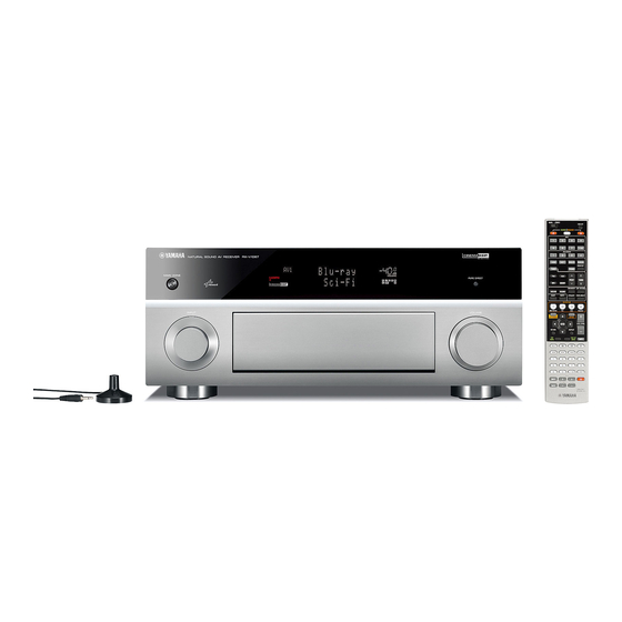
RX-V1067/HTR-8063/
Note:
When IC502 of NET P.C.B. or NET P.C.B. is replaced, the network function of this unit will not operate properly
without additional setting.
In such case, report the serial number of this unit to the following e-mail address.
Yamaha Corporation will reply providing the setting procedure to make the network function of this unit operate
properly.
注意:
NET P.C.B. および IC502(NET P.C.B.)を交換した場合、本機のネットワーク機能が正常に動作しません。
正常に動作させるための設定方法は、YCJ(Yamaha Corporation Japan)からご連絡します。
はじめに、交換した本機のシリアルナンバーを下記の E-mail アドレスへ報告してください。
This manual has been provided for the use of authorized YAMAHA Retailers and their service personnel.
It has been assumed that basic service procedures inherent to the industry, and more specifi cally YAMAHA Products, are already known
and understood by the users, and have therefore not been restated.
WARNING:
IMPORTANT:
The data provided is believed to be accurate and applicable to the unit(s) indicated on the cover. The research, engineering, and service
departments of YAMAHA are continually striving to improve YAMAHA products. Modifications are, therefore, inevitable and
specifi cations are subject to change without notice or obligation to retrofi t. Should any discrepancy appear to exist, please contact the
distributor's Service Division.
WARNING:
IMPORTANT:
■ CONTENTS
TO SERVICE PERSONNEL ............................................2
FRONT PANELS .........................................................3-4
REAR PANELS ...........................................................5-8
REMOTE CONTROL PANELS .......................................9
SPECIFICATIONS / 参考仕様 ................................. 10-15
INTERNAL VIEW .......................................................... 16
SERVICE PRECAUTIONS / サービス時の注意事項 ..... 16
DISASSEMBLY PROCEDURES / 分解手順 ........... 17-20
UPDATING FIRMWARE /
ファームウェアの書き込み .....................................21-22
AMP ADJUSTMENT / アンプ部調整 .......................23-25
ダイアグ(自己診断機能) .......................................26-67
1 0 1 1 8 3
SERVICE MANUAL
E-mail: ycav-ysiss@gmx.yamaha.com
IMPORTANT NOTICE
Failure to follow appropriate service and safety procedures when servicing this product may result in personal injury,
destruction of expensive components, and failure of the product to perform as specifi ed. For these reasons, we advise
all YAMAHA product owners that any service required should be performed by an authorized YAMAHA Retailer or
the appointed service representative.
The presentation or sale of this manual to any individual or fi rm does not constitute authorization, certifi cation or
recognition of any applicable technical capabilities, or establish a principle-agent relationship of any form.
Static discharges can destroy expensive components. Discharge any static electricity your body may have
accumulated by grounding yourself to the ground buss in the unit (heavy gauge black wires connect to this buss).
Turn the unit OFF during disassembly and part replacement. Recheck all work before you apply power to the unit.
DISPLAY DATA .......................................................68-70
IC DATA ...................................................................71-90
PIN CONNECTION DIAGRAMS .............................91-94
BLOCK DIAGRAMS ................................................95-99
PRINTED CIRCUIT BOARDS ............................. 100-126
SCHEMATIC DIAGRAMS ................................... 127-145
REPLACEMENT PARTS LIST ............................ 147-177
REMOTE CONTROL ........................................... 178-180
ADVANCED SETUP ............................................ 181-183
本機の基本設定 / 初期化を行う ........................... 184-185
Copyright © 2010
This manual is copyrighted by YAMAHA and may not be copied or
redistributed either in print or electronically without permission.
AV RECEIVER
RX-A1000
All rights reserved.
P.O.Box 1, Hamamatsu, Japan
'10.08
Advertisement
Table of Contents

Related Manuals for Yamaha HTR-8063


Summarization of Contents
To Service Personnel
Critical Components Information
Components with special characteristics marked ! must be replaced with identical parts.
Leakage Current Measurement (For 120V Models Only)
Verification of proper insulation from supply circuits after service completion.
About Lead-Free Solder
Information on lead-free solder types used and recommended for repair work.
Specifications
Audio Section
Detailed specifications for the audio output power and input sensitivity.
Video Section
Specifications for video signal types, conversion, and levels.
FM Section
Specifications for FM tuning range, sensitivity, and signal-to-noise ratio.
AM Section
Specifications for AM tuning range and antenna input.
General
General specifications including power supply, consumption, dimensions, and weight.
Set Menu Table
Speaker Setup
Configuration options for speaker settings like distance, level, and parametric EQ.
Sound Setup
Settings for audio synchronization and volume adjustments.
Video Setup
Settings for analog-to-analog conversion and processing.
Disassembly Procedures
Removal of Top Cover
Step-by-step instructions for removing the top cover.
Removal of Front Panel Unit and Sub-chassis Unit
Procedures for disassembling the front panel and sub-chassis units.
Updating Firmware
Confirmation of Firmware Version and Checksum
How to check firmware version and checksum before and after updating.
Initializing the Back-up IC (EEPROM: IC903 of the DIGITAL P.C.B.)
Procedure to initialize the backup IC after firmware update for proper memorization.
Amp Adjustment
Idling Current Adjustment
Steps to adjust idling current for all channels to specified voltage values.
DC Offset Confirmation
Confirmation that DC offset for all channels is within the specified range after adjustment.
When the Protection Function Worked to Turn Off the Power:
When There is a History of Protection Function Due to Excess Current
Cause and troubleshooting for protection function activation due to excessive current.
Details of Self-Diagnostic Function Menu
A1. DSP AUDIO
Menu to check the audio signal route via DSP, including sub-menus for margin and non-margin.
U2. USB (continued)
U3. INVALID ITEM
Placeholder for items not for service.
V2. DIGITAL VIDEO CHECK (continued)
P1. SYSTEM MONITOR
Menu to display A/D conversion values of microprocessor for panel keys and protection functions.
S2. SET INFORMATION (continued)
S3. FACTORY PRESET
Menu for reserving or inhibiting initialization of the backup IC (EEPROM).
DISPLAY DATA
PIN CONNECTION
Pin assignments for the V4001 component.
GRID ASSIGNMENT
Grid assignment for display segments.
PIN CONNECTION DIAGRAMS
ICs
Diagrams showing the pin configurations of various integrated circuits.
PIN CONNECTION DIAGRAMS (continued)
ICs (continued)
Continues diagrams showing the pin configurations of various integrated circuits.
PIN CONNECTION DIAGRAMS (continued)
Diodes
Diagrams showing the pin configurations of various diodes.
PIN CONNECTION DIAGRAMS (continued)
Transistors
Diagrams showing the pin configurations of various transistors.
BLOCK DIAGRAMS
AUDIO Section Block Diagram
Overall block diagram of the audio signal path.
BLOCK DIAGRAMS (continued)
DIGITAL P.C.B. Section Block Diagram
Block diagram illustrating the digital signal processing pathways.
BLOCK DIAGRAMS (continued)
HDMI/VIDEO Section Block Diagram
Block diagram showing the HDMI and video signal flow.
BLOCK DIAGRAMS (continued)
Power Supply and Protection Section Block Diagram
Block diagram illustrating the power supply and protection circuits.
BLOCK DIAGRAMS (continued)
NET P.C.B. Section Block Diagram
Block diagram of the Network Printed Circuit Board.
PRINTED CIRCUIT BOARDS
DIGITAL (1) P.C.B. (Side A)
Component layout diagram for the DIGITAL (1) PCB, side A.
PRINTED CIRCUIT BOARDS (continued)
DIGITAL (1) P.C.B. (Side B)
Component layout diagram for the DIGITAL (1) PCB, side B.
PRINTED CIRCUIT BOARDS (continued)
DIGITAL (2) P.C.B. (Side A)
Component layout diagram for the DIGITAL (2) PCB, side A.
DIGITAL (3) P.C.B. (Side A)
Component layout diagram for the DIGITAL (3) PCB, side A.
PRINTED CIRCUIT BOARDS (continued)
DIGITAL (2) P.C.B. (Side B)
Component layout diagram for the DIGITAL (2) PCB, side B.
DIGITAL (3) P.C.B. (Side B)
Component layout diagram for the DIGITAL (3) PCB, side B.
PRINTED CIRCUIT BOARDS (continued)
FUNCTION (1) P.C.B. (Side A)
Component layout diagram for the FUNCTION (1) PCB, side A.
PRINTED CIRCUIT BOARDS (continued)
FUNCTION (1) P.C.B. (Side B)
Component layout diagram for the FUNCTION (1) PCB, side B.
PRINTED CIRCUIT BOARDS (continued)
FUNCTION (2) P.C.B. (Side A)
Component layout diagram for the FUNCTION (2) PCB, side A.
FUNCTION (3) P.C.B. (Side A)
Component layout diagram for the FUNCTION (3) PCB, side A.
PRINTED CIRCUIT BOARDS (continued)
OPERATION (1) P.C.B. (Side A)
Component layout diagram for the OPERATION (1) PCB, side A.
PRINTED CIRCUIT BOARDS (continued)
OPERATION (1) P.C.B. (Side B)
Component layout diagram for the OPERATION (1) PCB, side B.
PRINTED CIRCUIT BOARDS (continued)
OPERATION (2) P.C.B. (Side A)
Component layout diagram for the OPERATION (2) PCB, side A.
OPERATION (3) P.C.B. (Side A)
Component layout diagram for the OPERATION (3) PCB, side A.
OPERATION (4) P.C.B. (Side A)
Component layout diagram for the OPERATION (4) PCB, side A.
PRINTED CIRCUIT BOARDS (continued)
OPERATION (2) P.C.B. (Side B)
Component layout diagram for the OPERATION (2) PCB, side B.
OPERATION (3) P.C.B. (Side B)
Component layout diagram for the OPERATION (3) PCB, side B.
OPERATION (4) P.C.B. (Side B)
Component layout diagram for the OPERATION (4) PCB, side B.
PRINTED CIRCUIT BOARDS (continued)
MAIN (1) P.C.B. (Side A)
Component layout diagram for the MAIN (1) PCB, side A.
MAIN (4) P.C.B. (Side A)
Component layout diagram for the MAIN (4) PCB, side A.
PRINTED CIRCUIT BOARDS (continued)
MAIN (1) P.C.B. (Side B)
Component layout diagram for the MAIN (1) PCB, side B.
MAIN (4) P.C.B. (Side B)
Component layout diagram for the MAIN (4) PCB, side B.
PRINTED CIRCUIT BOARDS (continued)
MAIN (2) P.C.B. (Side A)
Component layout diagram for the MAIN (2) PCB, side A.
MAIN (5) P.C.B. (Side A)
Component layout diagram for the MAIN (5) PCB, side A.
PRINTED CIRCUIT BOARDS (continued)
MAIN (2) P.C.B. (Side B)
Component layout diagram for the MAIN (2) PCB, side B.
MAIN (5) P.C.B. (Side B)
Component layout diagram for the MAIN (5) PCB, side B.
PRINTED CIRCUIT BOARDS (continued)
MAIN (3) P.C.B. (Side A)
Component layout diagram for the MAIN (3) PCB, side A.
PRINTED CIRCUIT BOARDS (continued)
MAIN (3) P.C.B. (Side B)
Component layout diagram for the MAIN (3) PCB, side B.
PRINTED CIRCUIT BOARDS (continued)
POWER (1) P.C.B. (Side A)
Component layout diagram for the POWER (1) PCB, side A.
PRINTED CIRCUIT BOARDS (continued)
POWER (1) P.C.B. (Side B)
Component layout diagram for the POWER (1) PCB, side B.
PRINTED CIRCUIT BOARDS (continued)
POWER (2) P.C.B. (Side A)
Component layout diagram for the POWER (2) PCB, side A.
POWER (3) P.C.B. (Side A)
Component layout diagram for the POWER (3) PCB, side A.
POWER (4) P.C.B. (Side A)
Component layout diagram for the POWER (4) PCB, side A.
PRINTED CIRCUIT BOARDS (continued)
POWER (2) P.C.B. (Side B)
Component layout diagram for the POWER (2) PCB, side B.
POWER (3) P.C.B. (Side B)
Component layout diagram for the POWER (3) PCB, side B.
POWER (4) P.C.B. (Side B)
Component layout diagram for the POWER (4) PCB, side B.
PRINTED CIRCUIT BOARDS (continued)
VIDEO (1) P.C.B. (Side A)
Component layout diagram for the VIDEO (1) PCB, side A.
PRINTED CIRCUIT BOARDS (continued)
VIDEO (1) P.C.B. (Side B)
Component layout diagram for the VIDEO (1) PCB, side B.
PRINTED CIRCUIT BOARDS (continued)
VIDEO (2) P.C.B. (Side A)
Component layout diagram for the VIDEO (2) PCB, side A.
VIDEO (3) P.C.B. (Side A)
Component layout diagram for the VIDEO (3) PCB, side A.
VIDEO (4) P.C.B. (Side A)
Component layout diagram for the VIDEO (4) PCB, side A.
VIDEO (5) P.C.B. (Side A)
Component layout diagram for the VIDEO (5) PCB, side A.
PRINTED CIRCUIT BOARDS (continued)
VIDEO (2) P.C.B. (Side B)
Component layout diagram for the VIDEO (2) PCB, side B.
VIDEO (3) P.C.B. (Side B)
Component layout diagram for the VIDEO (3) PCB, side B.
VIDEO (4) P.C.B. (Side B)
Component layout diagram for the VIDEO (4) PCB, side B.
VIDEO (5) P.C.B. (Side B)
Component layout diagram for the VIDEO (5) PCB, side B.
PRINTED CIRCUIT BOARDS (continued)
NET P.C.B. (Side A)
Component layout diagram for the NET PCB, side A.
NET P.C.B. (Side B)
Component layout diagram for the NET PCB, side B.
SCHEMATIC DIAGRAMS
DIGITAL 1/8
Schematic diagram for the DIGITAL section, page 1 of 8.
SCHEMATIC DIAGRAMS (continued)
DIGITAL 2/8
Schematic diagram for the DIGITAL section, page 2 of 8.
SCHEMATIC DIAGRAMS (continued)
DIGITAL 3/8
Schematic diagram for the DIGITAL section, page 3 of 8.
SCHEMATIC DIAGRAMS (continued)
DIGITAL 4/8
Schematic diagram for the DIGITAL section, page 4 of 8.
SCHEMATIC DIAGRAMS (continued)
DIGITAL 5/8
Schematic diagram for the DIGITAL section, page 5 of 8.
SCHEMATIC DIAGRAMS (continued)
DIGITAL 6/8
Schematic diagram for the DIGITAL section, page 6 of 8.
SCHEMATIC DIAGRAMS (continued)
DIGITAL 7/8
Schematic diagram for the DIGITAL section, page 7 of 8.
SCHEMATIC DIAGRAMS (continued)
DIGITAL 8/8
Schematic diagram for the DIGITAL section, page 8 of 8.
REPLACEMENT PARTS LIST
ELECTRICAL COMPONENT PARTS
List of electrical components with their part numbers and descriptions.
REPLACEMENT PARTS LIST (continued)
P.C.B. DIGITAL
List of replacement parts for the DIGITAL P.C.B.
REPLACEMENT PARTS LIST (continued)
P.C.B. DIGITAL (continued)
List of replacement parts for the DIGITAL P.C.B.
REPLACEMENT PARTS LIST (continued)
P.C.B. DIGITAL (continued)
List of replacement parts for the DIGITAL P.C.B.
REPLACEMENT PARTS LIST (continued)
P.C.B. DIGITAL (continued)
List of replacement parts for the DIGITAL P.C.B.
REPLACEMENT PARTS LIST (continued)
P.C.B. DIGITAL (continued)
List of replacement parts for the DIGITAL P.C.B.
REPLACEMENT PARTS LIST (continued)
P.C.B. DIGITAL (continued)
List of replacement parts for the DIGITAL P.C.B.
REPLACEMENT PARTS LIST (continued)
P.C.B. DIGITAL (continued)
List of replacement parts for the DIGITAL P.C.B.
REPLACEMENT PARTS LIST (continued)
P.C.B. DIGITAL and P.C.B. OPERATION
List of replacement parts for DIGITAL and OPERATION P.C.B.s.
REPLACEMENT PARTS LIST (continued)
P.C.B. OPERATION
List of replacement parts for the OPERATION P.C.B.
REPLACEMENT PARTS LIST (continued)
P.C.B. FUNCTION
List of replacement parts for the FUNCTION P.C.B.
REPLACEMENT PARTS LIST (continued)
P.C.B. FUNCTION (continued)
List of replacement parts for the FUNCTION P.C.B.
REPLACEMENT PARTS LIST (continued)
P.C.B. MAIN
List of replacement parts for the MAIN P.C.B.
REPLACEMENT PARTS LIST (continued)
P.C.B. MAIN (continued)
List of replacement parts for the MAIN P.C.B.
REPLACEMENT PARTS LIST (continued)
P.C.B. MAIN (continued)
List of replacement parts for the MAIN P.C.B.
REPLACEMENT PARTS LIST (continued)
P.C.B. MAIN (continued)
List of replacement parts for the MAIN P.C.B.
REPLACEMENT PARTS LIST (continued)
P.C.B. MAIN (continued)
List of replacement parts for the MAIN P.C.B.
REPLACEMENT PARTS LIST (continued)
P.C.B. MAIN (continued)
List of replacement parts for the MAIN P.C.B.
REPLACEMENT PARTS LIST (continued)
P.C.B. MAIN (continued)
List of replacement parts for the MAIN P.C.B.
REPLACEMENT PARTS LIST (continued)
P.C.B. MAIN (continued)
List of replacement parts for the MAIN P.C.B.
REPLACEMENT PARTS LIST (continued)
P.C.B. POWER
List of replacement parts for the POWER P.C.B.
REPLACEMENT PARTS LIST (continued)
P.C.B. POWER and P.C.B. VIDEO
List of replacement parts for POWER and VIDEO P.C.B.s.
REPLACEMENT PARTS LIST (continued)
P.C.B. VIDEO
List of replacement parts for the VIDEO P.C.B.
REPLACEMENT PARTS LIST (continued)
P.C.B. VIDEO (continued)
List of replacement parts for the VIDEO P.C.B.
REPLACEMENT PARTS LIST (continued)
P.C.B. VIDEO and P.C.B. NET
List of replacement parts for VIDEO and NET P.C.B.s.
REPLACEMENT PARTS LIST (continued)
P.C.B. NET
List of replacement parts for the NET P.C.B.
REMOTE CONTROL
PANELS
Diagrams of the different remote control panels (RAV346, RAV347, RAV348).
KEY NO. LAYOUT
FUNCTION CODE
Table mapping key numbers to functions and codes for remote control programming.
ADVANCED SETUP (continued)
Resetting the SIRIUS Satellite / tuner Code (U model)
Instructions for resetting SIRIUS or tuner codes on U model units.
Removing HDMI Video Output Scaling Limits
How to remove HDMI video output scaling limitations.
Recovery and Backup of the System Settings
Procedures for backing up and recovering system settings.
Initializing Various Settings for This Unit
Steps to initialize various settings to their default factory settings.
本機の設定を変更する
アドバンストセットアップメニューの更新
Procedures for updating advanced setup menu settings.
リモコン ID の変更
How to change or set the remote control ID.
Need help?
Do you have a question about the HTR-8063 and is the answer not in the manual?
Questions and answers