Table of Contents
Advertisement
RX-V640/RX-V640RDS/HTR-5660/DSP-AX640/DSP-AX640SE
This manual has been provided for the use of authorized YAMAHA Retailers and their service personnel.
It has been assumed that basic service procedures inherent to the industry, and more specifically YAMAHA Products, are already
known and understood by the users, and have therefore not been restated.
WARNING:
IMPORTANT:
The data provided is believed to be accurate and applicable to the unit(s) indicated on the cover. The research, engineering, and
service departments of YAMAHA are continually striving to improve YAMAHA products. Modifications are, therefore, inevitable
and specifications are subject to change without notice or obligation to retrofit. Should any discrepancy appear to exist, please
contact the distributor's Service Division.
WARNING:
IMPORTANT:
I CONTENTS
TO SERVICE PERSONNEL .......................................... 2
IMPEDANCE SELECTOR ............................................. 2
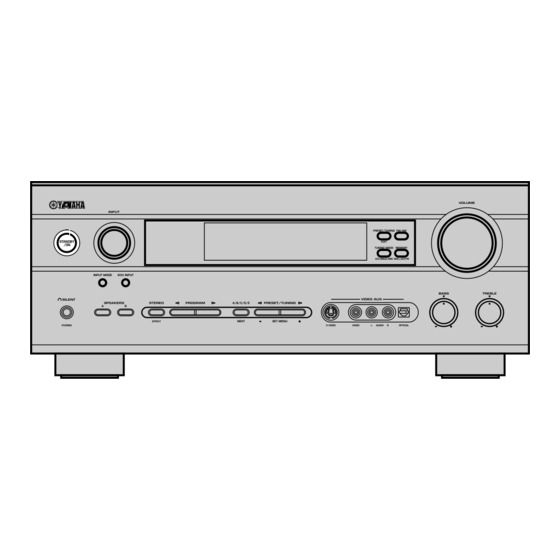
FRONT PANELS ........................................................ 3~5
REAR PANELS ........................................................ 6~12
REMOTE CONTROL PANELS .................................... 13
SPECIFICATIONS / 参考仕様 ................................ 14~17
INTERNAL VIEW ......................................................... 18
DISASSEMBLY PROCEDURES / 分解手順 ......... 19~22
自己診断機能(ダイアグ) ..................................... 23~44
1 0 0 8 4 7
AV RECEIVER/AV AMPLIFIER
RX-V740/RX-V740RDS/DSP-AX740
IMPORTANT NOTICE
Failure to follow appropriate service and safety procedures when servicing this product may result in personal
injury, destruction of expensive components, and failure of the product to perform as specified. For these reasons,
we advise all YAMAHA product owners that any service required should be performed by an authorized
YAMAHA Retailer or the appointed service representative.
The presentation or sale of this manual to any individual or firm does not constitute authorization, certification or
recognition of any applicable technical capabilities, or establish a principle-agent relationship of any form.
Static discharges can destroy expensive components. Discharge any static electricity your body may have
accumulated by grounding yourself to the ground buss in the unit (heavy gauge black wires connect to this buss).
Turn the unit OFF during disassembly and part replacement. Recheck all work before you apply power to the unit.
SERVICE MANUAL
AMP ADJUSTMENT / アンプ部調整 ........................... 45
DISPLAY DATA ..................................................... 46~47
IC DATA ................................................................. 48~53
BLOCK DIAGRAM ................................................. 54~55
PRINTED CIRCUIT BOARD .................................. 56~79
PIN CONNECTION DIAGRAM .................................... 80
SCHEMATIC DIAGRAM ........................................ 81~92
PARTS LIST ......................................................... 93~147
REMOTE CONTROL .......................................... 148~152
P.O.Box 1, Hamamatsu, Japan
Advertisement
Table of Contents

Related Manuals for Yamaha DSP-AX740


Summarization of Contents
IMPORTANT NOTICE
WARNING: Service Safety
Warns of personal injury and component damage from improper servicing.
IMPORTANT: Manual Authorization
Clarifies manual distribution does not grant service authorization.
WARNING: Static Discharge
Advises grounding to prevent static discharge damage.
IMPORTANT: Power Off & Recheck
Emphasizes powering off for disassembly and rechecking work.
TO SERVICE PERSONNEL
Critical Components
Highlights special components marked 's' requiring exact replacement.
Leakage Current Measurement
Details verifying insulation of exposed surfaces for safety after service.
IMPEDANCE SELECTOR
WARNING: Impedance Selector
Warns against changing the impedance selector while the unit is powered on to prevent damage.
SPECIFICATIONS / 参考仕様
Audio Section / オーディオ部
Details RMS output power, frequency response, distortion, and tone control characteristics.
Video Section / ビデオ部
Specifies video signal types, levels, and frequency response.
FM Section / FM部
Lists tuning range, sensitivity, selectivity, and frequency response for FM reception.
AM Section / AM部
Details tuning range and usable sensitivity for AM reception.
General / 総合
Covers power supply voltage, power consumption, and standby power consumption.
DISASSEMBLY PROCEDURES / 分解手順
Removal of Top Cover
Step-by-step instructions for removing the top cover.
Removal of Front Panel
Instructions for removing the front panel assembly.
Removal of Sub Chassis
Steps to remove the sub chassis, including side plates and connectors.
Removal of DSP P.C.B.
Details on removing the DSP P.C.B. with its support and connectors.
Removal of FUNCTION (1) ~ (7) P.C.B.s and Tuner
Instructions for removing various FUNCTION P.C.B.s and the tuner.
When checking the P.C.B.
Guidelines for checking P.C.B.s, including reconnecting cables and grounding.
Removal of MAIN (1), MAIN (3) and POWER (1) P.C.B.s
Steps for removing MAIN (1), MAIN (3), and POWER (1) P.C.B.s.
SELF DIAGNOSIS FUNCTION (DIAG) / 自己診断機能(ダイアグ)
DIAG Menu Items
Lists the 15 DIAG menu items and their sub-menu options for diagnostics.
Starting DIAG
Explains how to initiate the DIAG mode by pressing specific keys.
Starting DIAG in the protection cancel mode
Details entering DIAG mode with protection functions disabled.
Canceling DIAG
Procedure for canceling DIAG mode and restoring settings.
Functions in DIAG mode
Explains the operational capabilities available within the DIAG mode.
Operation procedure of DIAG menu and SUB-MENU
Explains how to navigate and select DIAG menus and sub-menus.
Initial settings used to start DIAG
Lists the default settings applied when starting the DIAG mode.
Details of DIAG menu
1. DSP THROUGH
Explains the DSP THROUGH function, including Analog Bypass and YSS modes.
ANALOG BYPASS
Details how the signal bypasses the DSP section for direct output.
YSS 0dB
Describes YSS 0dB output, including head margin information.
YSS Front 0dB
Details YSS Front 0dB output for front CH signals to the main CH.
YSS FULL BIT
Describes the YSS FULL BIT output, which excludes head margin.
YSS FULL BIT F
Details the YSS FULL BIT F output for front CH signals to the main CH.
2. RAM THROUGH
Explains the RAM THROUGH function for YSS938, outputting CT signal via Sub DSP-DRAM.
3. PRO LOGIC
Details the PRO LOGIC processing, including output through Sub DSP-DRAM and available modes.
Neo:6
Explains the Neo:6 processing, its fixed mode, and signal handling for DD/dts and AAC inputs.
10. AD DATA CHECK/FAN TEST
DC/PS (protection detection)
Explains protection detection values for DC output and power supply.
THM/Fan (temperature detection/fan drive level)
Details temperature detection and fan drive level monitoring.
11. IF STATUS (Input function status)
<5th byte> Signal processing status information
Provides signal processing status information, including mute requests and DTS flashing status.
CS1-5: Indicates channel status information of the input signal (IEC60958).
Shows channel status information for the input signal according to IEC60958.
AMP ADJUSTMENT / アンプ部調整
Confirmation of Idling Current of Main (1) P. C. B.
Details checking idling current of main P.C.B. by measuring terminal voltages.
Attention
Advises checking for defective components before cutting bias resistors after repair.
DISPLAY DATA
PIN CONNECTION
Diagram showing pin numbers and their corresponding connections.
GRID ASSIGNMENT
Illustration of grid assignments for the display.
IC DATA
IC601: M30626FHPFP (FUNCTION P.C.B.)
Details the functionality and I/O of the M30626FHPFP IC on the FUNCTION P.C.B.
IC608 : XC9527XL-100100 (DSP P.C.B.)
Details the functionality and I/O of the XC9527XL-100100 PLD on the DSP P.C.B.
IC601 : YSS938 (DSP P.C.B.)
Pin connection and function details for the YSS938 IC on the DSP P.C.B.
PRINTED CIRCUIT BOARD (Foil side)
DSP P. C. B. (Lead Type Device)
Shows component layout on the DSP P.C.B. for lead type devices.
DSP P. C. B. (Surface Mount Device)
Illustrates component placement on the DSP P.C.B. for surface mount devices.
FUNCTION (1) P. C. B. (Lead Type Device)
Component layout diagram for the FUNCTION (1) P.C.B. (lead type).
FUNCTION (2) P. C. B. (Lead Type Device)
Component layout diagram for the FUNCTION (2) P.C.B. (lead type).
FUNCTION (3) P. C. B. (Lead Type Device)
Component layout diagram for the FUNCTION (3) P.C.B. (lead type).
FUNCTION (4) P. C. B. (Surface Mount Device)
Component layout diagram for the FUNCTION (4) P.C.B. (surface mount).
FUNCTION (5) P. C. B. (Surface Mount Device)
Component layout diagram for the FUNCTION (5) P.C.B. (surface mount).
FUNCTION (6) P. C. B. (Surface Mount Device)
Component layout diagram for the FUNCTION (6) P.C.B. (surface mount).
FUNCTION (7) P. C. B. (Surface Mount Device)
Component layout diagram for the FUNCTION (7) P.C.B. (surface mount).
FUNCTION (8) P. C. B. (Lead Type Device)
Component layout diagram for the FUNCTION (8) P.C.B. (lead type).
OPERATION (1) P. C. B. (Lead Type Device)
Component layout diagram for the OPERATION (1) P.C.B. (lead type).
OPERATION (3) P. C. B. (Lead Type Device)
Component layout diagram for the OPERATION (3) P.C.B. (lead type).
OPERATION (2) P. C. B. (Lead Type Device)
Component layout diagram for the OPERATION (2) P.C.B. (lead type).
OPERATION (4) P. C. B. (Lead Type Device)
Component layout diagram for the OPERATION (4) P.C.B. (lead type).
OPERATION (5) P. C. B. (Lead Type Device)
Component layout diagram for the OPERATION (5) P.C.B. (lead type).
OPERATION (6) P. C. B. (Lead Type Device)
Component layout diagram for the OPERATION (6) P.C.B. (lead type).
OPERATION (7) P. C. B. (Lead Type Device)
Component layout diagram for the OPERATION (7) P.C.B. (lead type).
OPERATION (4) P. C. B. (Surface Mount Device)
Component layout diagram for the OPERATION (4) P.C.B. (surface mount).
OPERATION (5) P. C. B. (Surface Mount Device)
Component layout diagram for the OPERATION (5) P.C.B. (surface mount).
OPERATION (6) P. C. B. (Surface Mount Device)
Component layout diagram for the OPERATION (6) P.C.B. (surface mount).
OPERATION (7) P. C. B. (Surface Mount Device)
Component layout diagram for the OPERATION (7) P.C.B. (surface mount).
OPERATION (1) P. C. B. (Lead Type Device)
Component layout diagram for the OPERATION (1) P.C.B. (lead type).
OPERATION (3) P. C. B. (Lead Type Device)
Component layout diagram for the OPERATION (3) P.C.B. (lead type).
OPERATION (2) P. C. B. (Lead Type Device)
Component layout diagram for the OPERATION (2) P.C.B. (lead type).
OPERATION (1) P. C. B. (Surface Mount Device)
Component layout diagram for the OPERATION (1) P.C.B. (surface mount).
OPERATION (4) P. C. B. (Lead Type Device)
Component layout diagram for the OPERATION (4) P.C.B. (lead type).
OPERATION (6) P. C. B. (Lead Type Device)
Component layout diagram for the OPERATION (6) P.C.B. (lead type).
OPERATION (5) P. C. B. (Lead Type Device)
Component layout diagram for the OPERATION (5) P.C.B. (lead type).
OPERATION (4) P. C. B. (Surface Mount Device)
Component layout diagram for the OPERATION (4) P.C.B. (surface mount).
OPERATION (1) P. C. B. (Surface Mount Device)
Component layout diagram for the OPERATION (1) P.C.B. (surface mount).
OPERATION (4) P. C. B. (Lead Type Device)
Component layout diagram for the OPERATION (4) P.C.B. (lead type).
OPERATION (5) P. C. B. (Lead Type Device)
Component layout diagram for the OPERATION (5) P.C.B. (lead type).
OPERATION (6) P. C. B. (Lead Type Device)
Component layout diagram for the OPERATION (6) P.C.B. (lead type).
OPERATION (7) P. C. B. (Lead Type Device)
Component layout diagram for the OPERATION (7) P.C.B. (lead type).
OPERATION (4) P. C. B. (Surface Mount Device)
Component layout diagram for the OPERATION (4) P.C.B. (surface mount).
OPERATION (5) P. C. B. (Surface Mount Device)
Component layout diagram for the OPERATION (5) P.C.B. (surface mount).
OPERATION (6) P. C. B. (Surface Mount Device)
Component layout diagram for the OPERATION (6) P.C.B. (surface mount).
OPERATION (7) P. C. B. (Surface Mount Device)
Component layout diagram for the OPERATION (7) P.C.B. (surface mount).
OPERATION (1) P. C. B. (Surface Mount Device)
Component layout diagram for the OPERATION (1) P.C.B. (surface mount).
OPERATION (4) P. C. B. (Lead Type Device)
Component layout diagram for the OPERATION (4) P.C.B. (lead type).
OPERATION (1) P. C. B. (Lead Type Device)
Component layout diagram for the OPERATION (1) P.C.B. (lead type).
OPERATION (3) P. C. B. (Lead Type Device)
Component layout diagram for the OPERATION (3) P.C.B. (lead type).
OPERATION (4) P. C. B. (Lead Type Device)
Component layout diagram for the OPERATION (4) P.C.B. (lead type).
OPERATION (1) P. C. B. (Lead Type Device)
Component layout diagram for the OPERATION (1) P.C.B. (lead type).
OPERATION (2) P. C. B. (Lead Type Device)
Component layout diagram for the OPERATION (2) P.C.B. (lead type).
OPERATION (3) P. C. B. (Lead Type Device)
Component layout diagram for the OPERATION (3) P.C.B. (lead type).
OPERATION (4) P. C. B. (Lead Type Device)
Component layout diagram for the OPERATION (4) P.C.B. (lead type).
OPERATION (1) P. C. B. (Lead Type Device)
Component layout diagram for the OPERATION (1) P.C.B. (lead type).
OPERATION (3) P. C. B. (Lead Type Device)
Component layout diagram for the OPERATION (3) P.C.B. (lead type).
PIN CONNECTION DIAGRAM
Diagrams showing pin connections for ICs, diodes, and transistors.
ICs
Diagrams showing pin connections for various ICs.
Diodes
Diagrams illustrating diode pin connections.
Transistors
Diagrams showing pin connections for various transistors.
SCHEMATIC DIAGRAM (DSP)
Detailed circuit diagram for the DSP section, including ICs, regulators, and memory components.
SCHEMATIC DIAGRAM (FUNCTION 1/2)
Detailed circuit diagram for the FUNCTION section, covering input selectors, volume control, and mute circuits.
SCHEMATIC DIAGRAM (FUNCTION 2/2)
Continues the FUNCTION schematic, illustrating video drivers, display controllers, and microcontrollers.
SCHEMATIC DIAGRAM (FUNCTION 1/2)
Detailed circuit diagram for the FUNCTION section, covering input selectors, volume control, and mute circuits.
SCHEMATIC DIAGRAM (FUNCTION 2/2)
Continues the FUNCTION schematic, illustrating video drivers, display controllers, and microcontrollers.
SCHEMATIC DIAGRAM (FUNCTION 1/2)
Detailed circuit diagram for the FUNCTION section, covering input selectors, volume control, and mute circuits.
SCHEMATIC DIAGRAM (FUNCTION 2/2)
Continues the FUNCTION schematic, illustrating video drivers, display controllers, and microcontrollers.
SCHEMATIC DIAGRAM (OPERATION)
Circuit diagrams for the operation section, including FL driver, IR remote, and headphone amplifier.
SCHEMATIC DIAGRAM (OPERATION)
Continues the operation schematic, showing circuits for tuner, CD, and input selectors.
SCHEMATIC DIAGRAM (VIDEO)
Circuit diagram detailing the video input and output paths, including selectors and amplifiers.
SCHEMATIC DIAGRAM (MAIN)
Circuit diagrams for the main power amplifier stages (L, R, C, Rear L/R) and regulators.
SCHEMATIC DIAGRAM (POWER)
Circuit diagrams for the power supply section, including transformers, relays, and voltage selectors.
PARTS LIST
List of all parts used in the unit, categorized by type.
ELECTRICAL PARTS
Lists electrical components like capacitors, connectors, coils, diodes, and resistors with abbreviations.
Chip Resistors
Lists chip resistors with their part numbers, descriptions, and values.
Parts List for Carbon Resistors
Lists carbon resistors by value, part number, and type.
MECHANICAL PARTS
Lists mechanical parts such as front panels, escutcheons, screws, and connectors.
EXPLODED VIEW
Exploded view diagram showing the assembly of the unit's mechanical parts.
ACCESSORIES
Lists accessories included with the unit, such as remote control, battery, and antennas.
MECHANICAL PARTS
Lists mechanical parts such as front panels, escutcheons, P.C.B.s, buttons, and connectors.
ACCESSORIES
Lists accessories included with the unit, such as remote control, battery, and antennas.
MECHANICAL PARTS
Lists mechanical parts for the DSP-AX640SE, including front panels, P.C.B.s, buttons, and connectors.
ACCESSORIES
Lists accessories included with the unit, such as remote control and battery.
REMOTE CONTROL RAV244, RAV237
Schematic diagram of the remote control unit showing button layout and internal circuitry.
REMOTE CONTROL RAV244, 245
Diagram illustrating the pin connections for the remote control unit.
REMOTE CONTROL RAV244, RAV237
Table mapping button functions to schematic key codes and internal signals.
REMOTE CONTROL RAV244, 245
Circuit diagram showing the internal components and connections of the remote control unit.
REMOTE CONTROL RAV244, RAV237
Table mapping button functions to schematic key codes and internal signals for various models.
Need help?
Do you have a question about the DSP-AX740 and is the answer not in the manual?
Questions and answers