Table of Contents
Advertisement
QQ
3 7 63 1515 0
SERVICE MANUAL
Ver. 1.4 2006.03
TE
L 13942296513
System
Compact disc digital audio system
Laser diode properties
Emission duration: Continuous
Laser output: Less than 44.6 µW (This output is the value measured at a
distance of 200 mm from the objective lens surface on the optical pick-up
block with 7 mm aperture.)
Power requirements
• Two LR6 (size AA) batteries: 1.5 V DC × 2
• AC power adaptor (DC IN 4.5 V jack):
220 V, 50 Hz (NE005: EE,EU8/NE006: EU8, EE, E18)
120 V, 60 Hz (C&SA, MX)
Dimensions (w/h/d) (without projecting parts and controls)
Approx. 139.8 × 28.8 × 139.8 mm
Mass (excluding accessories)
Approx. 200 g
Operating temperature
5°C - 35°C
MPEG Layer-3 audio coding technology and patents licensed from
Fraunhofer IIS and Thomson.
Design and specifications are subject to change without notice.
Supplied accessories
AC power adaptor (1)
(NE005: EE, EU8/NE0050: C&SA, MX/NE006: EU8, EE, E18)
Headphones (1)
Remote control (1) (supplied with D-NE006 only)
www
.
Sony Corporation
9-879-861-05
Personal Audio Division
2006C02-1
Published by Sony Techno Create Corporation
© 2006.03
http://www.xiaoyu163.com
x
ao
u163
y
i
http://www.xiaoyu163.com
D-NE004/NE005/
2 9
8
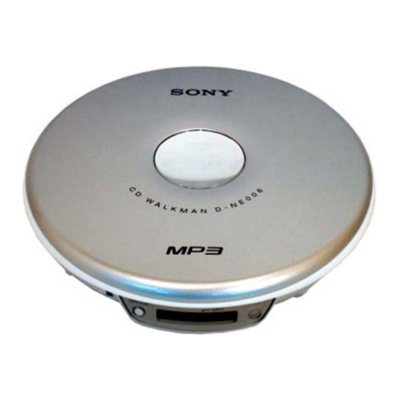
Photo: D-NE006
Model Name Using Similar Mechanism
CD Mechanism Type
Optical Pick-up Name
SPECIFICATIONS
Q Q
3
6 7
1 3
1 5
Battery life* (approx. hours)
(When the CD player is used on a flat and stable place.)
Playing time varies depending on how the CD player is used.
When using two Sony alkaline batteries LR6 (SG)
(produced in Japan)
G-PROTECTION
Audio CD
MP3 CD (Recorded at 128 kbps)
* Measured value by the standard of JEITA (Japan Electronics and
Information Technology Industries Association).
• The indicator sections of
power. One section does not always indicate one-fourth of the battery
power.
co
.
NE0050/NE006
9 4
2 8
US Model
Canadian Model
AEP Model
D-NE004/NE005/NE006
UK Model
E Model
D-NE005/NE0050/NE006
Australian Model
Tourist Model
NEW
CDM-3525A/3525AJ
DAX-25E
0 5
8
2 9
9 4
2 8
G-on
16
23
roughly show the remaining battery
m
PORTABLE CD PLAYER
9 9
D-NE005
D-NE004
D-NE005
D-NE006
9 9
G-off
11
23
Advertisement
Table of Contents

Related Manuals for Sony D-NE0050


Summary of Contents for Sony D-NE0050
- Page 1 Laser diode properties Playing time varies depending on how the CD player is used. Emission duration: Continuous When using two Sony alkaline batteries LR6 (SG) Laser output: Less than 44.6 µW (This output is the value measured at a (produced in Japan)
-
Page 2: Table Of Contents
REPLACE THESE COMPONENTS WITH SONY PARTS WHOSE FONCTIONNEMENT. NE REMPLACER CES COMPOSANTS PART NUMBERS APPEAR AS SHOWN IN THIS MANUAL OR IN QUE PAR DES PIÈSES SONY DONT LES NUMÉROS SONT SUPPLEMENTS PUBLISHED BY SONY. DONNÉS DANS CE MANUEL OU DANS LES SUPPÉMENTS PUBLIÉS PAR SONY. -
Page 3: Servicing Notes
D-NE004/NE005/NE0050/NE006 Ver. 1.2 SECTION 1 3 7 63 1515 0 SERVICING NOTES • Method: NOTES ON HANDLING THE OPTICAL PICK-UP Emission of the laser diode is visually checked. BLOCK OR BASE UNIT 1. Open the upper lid. The laser diode in the optical pick-up block may suffer electrostatic 2. -
Page 4: Disassembly
D-NE004/NE005/NE0050/NE006 SECTION 3 3 7 63 1515 0 DISASSEMBLY • This set can be disassembled in the order shown below. 3-1. DISASSEMBLY FLOW 3-2. UPPER LID ASSY, CABINET (MIDDLE) ASSY, CABINET (LOWER) ASSY (Page 4) 3-3. OPTICAL PICK-UP (CDM-3525A) (Page 5) 3-4. -
Page 5: Optical Pick-Up (Cdm-3525A)
D-NE004/NE005/NE0050/NE006 3 7 63 1515 0 3-3. OPTICAL PICK-UP (CDM-3525A) 3 optical pick-up (CDM-3525A) 1 CN501 2 Unsolder four lead wires To/From Optical pick-up (CDM-3525A) MAIN Board (side A) cabinet (lower) assy L 13942296513 3-4. JACK BOARD, MAIN BOARD •... -
Page 6: Lpf Board
D-NE004/NE005/NE0050/NE006 3 7 63 1515 0 3-5. LPF BOARD 1 Unsolder six lead wires TP307 C103(+) AUGND2 TP844 LPF Board TP842 SEG5 TP843 DVDD TP841 CDM4 2 cushion 3 LPF board 4 adhesive sheet MAIN Board (side B) MAIN Board (side A) -
Page 7: Test Mode
D-NE004/NE005/NE0050/NE006 SECTION 4 SECTION 5 3 7 63 1515 0 TEST MODE ELECTRICAL ADJUSTMENTS Procedure: The CD section adjustments are done automatically in this set. 1. Make a solder bridge to short SL803 (TEST) on the MAIN board side B. -
Page 8: Diagrams
D-NE004/NE005/NE0050/NE006 Ver. 1.2 SECTION 6 3 7 63 1515 0 DIAGRAMS • Note for Printed Wiring Boards and Schematic Diagrams Note on Printed Wiring Boards. Note on Schematic Diagrams. • All capacitors are in µF unless otherwise noted. (p: pF) 50 WV or •... -
Page 9: Block Diagram
D-NE004/NE005/NE0050/NE006 Ver. 1.2 3 7 6 3 1 5 1 5 0 6-1. BLOCK DIAGRAM IC602 SDRAM(16M) SEG5 DQ00-07 L.P.F COM4 A0-11 Q101 – 104 2,3,5,6,8,9,11,12,39, 19-24,27-32 17 16 15 14 36 35 34 40,42,43,45,46,48,49 IC301 Q602 HEADPHONE AMP... -
Page 10: Printed Wiring Board - Main Board (Side A), Lpf Board (Side A)
D-NE004/NE005/NE0050/NE006 Ver. 1.3 6-2. PRINTED WIRING BOARD – MAIN BOARD (SIDE A), LPF BOARD (SIDE A) – :Uses unleaded solder. 3 7 6 3 1 5 1 5 0 MAIN BOARD (SIDE A) • Semiconductor Location RB305 RB302 Ref. No. -
Page 11: Printed Wiring Board - Main Board (Side B), Lpf Board (Side B), Jack Board
D-NE004/NE005/NE0050/NE006 Ver. 1.3 6-3. PRINTED WIRING BOARD – MAIN BOARD (SIDE B), LPF BOARD (SIDE B), JACK BOARD – :Uses unleaded solder. 3 7 6 3 1 5 1 5 0 (AEP,EE,EU8,JE) MAIN BOARD (SIDE B) J302 JACK BOARD LINE OUT •... -
Page 12: Schematic Diagram - Main Board (1/2), Jack Board (1/2)
D-NE004/NE005/NE0050/NE006 Ver. 1.2 6-4. SCHEMATIC DIAGRAM – MAIN BOARD (1/2) , JACK BOARD (1/2) – • See page 8 for Waveforms. • See page 14 for IC Block Diagrams. 3 7 6 3 1 5 1 5 0 3525AJ... -
Page 13: Schematic Diagram - Main Board (2/2), Lpf Board, Jack Board (2/2)
D-NE004/NE005/NE0050/NE006 Ver. 1.2 6-5. SCHEMATIC DIAGRAM – MAIN BOARD (2/2), LPF BOARD, JACK BOARD (2/2) – • See page 8 for Waveforms. • See page 15 for IC Pin Function Description. 3 7 6 3 1 5 1 5 0... - Page 14 D-NE004/NE005/NE0050/NE006 Ver. 1.2 • IC Block Diagrams 3 7 6 3 1 5 1 5 0 IC601 BU9541AKV IC301 BH3544F-FE2 BIAS AVDD1 D CLASS HP LINE MUTE AMPLIFIER AMPLIFIER DGND2 TEST VBIAS RESETB SIGNAL 1 BIT DAC AGND1 CLK88...
-
Page 15: Ic Pin Function Description
D-NE004/NE005/NE0050/NE006 Ver. 1.2 3 7 63 1515 0 6-6. IC PIN FUNCTION DESCRIPTION • IC801 BU18704-S1 (SYSTEM CONTROLLER) Pin No. Pin name Description SEG0 Not used (OPEN) 2 to 21 SEG1 to SEG20 LCD segment output XLINEOUT_MUTE LINE OUT muting output... - Page 16 D-NE004/NE005/NE0050/NE006 3 7 63 1515 0 Pin No. Pin name Description BATT+ Batt+ terminal voltage monitoring input KEY1 Key matrix detect input KEY2 Key matrix detect input TEST MODE Test mode terminal WREM Wired remotecontroler key detection input (D-NE006 only)
-
Page 17: Exploded Views
D-NE004/NE005/NE0050/NE006 Ver. 1.3 SECTION 7 3 7 63 1515 0 EXPLODED VIEWS NOTE: The components identified by mark 0 • -XX and -X mean standardized parts, so they • Color Indication of Appearance Parts Example: or dotted line with mark 0 are critical may have some difference from the original KNOB, BALANCE (WHITE) . -
Page 18: Cabinet (Lower) Section
D-NE004/NE005/NE0050/NE006 Ver. 1.4 3 7 63 1515 0 7-2. CABINET (LOWER) SECTION not supplied not supplied Refer to supplement-1 page 2 for distinguish the type of the main board. Ref. No. Part No. Description Remark Ref. No. Part No. -
Page 19: Electrical Parts List
D-NE004/NE005/NE0050/NE006 Ver. 1.3 SECTION 8 JACK MAIN 3 7 63 1515 0 ELECTRICAL PARTS LIST NOTE: The components identified by mark 0 • SEMICONDUCTORS • Due to standardization, replacements in the or dotted line with mark 0 are critical In each case, u: µ, for example:... - Page 20 D-NE004/NE005/NE0050/NE006 Ver. 1.2 MAIN 3 7 63 1515 0 Ref. No. Part No. Description Remark Ref. No. Part No. Description Remark < CAPACITOR > C620 1-164-156-11 CERAMIC CHIP 0.1uF C101 1-162-966-11 CERAMIC CHIP 0.0022uF 10% C623 1-119-941-41 ELECT 470uF 6.3V...
- Page 21 D-NE004/NE005/NE0050/NE006 Ver. 1.3 MAIN 3 7 63 1515 0 Ref. No. Part No. Description Remark Ref. No. Part No. Description Remark IC601 6-708-763-01 IC BU9541AKV R405 1-218-873-11 METAL CHIP 0.5% 1/10W IC602 6-708-188-01 IC M12L16161A-7T (G) R406 1-216-833-11 METAL CHIP...
- Page 22 D-NE004/NE005/NE0050/NE006 Ver. 1.3 MAIN 3 7 63 1515 0 Ref. No. Part No. Description Remark Ref. No. Part No. Description Remark R829 1-216-845-11 METAL CHIP 100K 1/10W ACCESSORIES R835 1-414-760-21 FERRITE, EMI (SMD) (1608) ************ R843 1-216-833-11 METAL CHIP...
- Page 23 UK Model Ver. 1.3 D-NE004 E Model D-NE005/NE0050/NE006 Australian Model D-NE005 SUPPLEMENT-1 Tourist Model D-NE006 File this supplement with the service manual. Subject : • CHANGE OF MAIN BOARD • ADDITION OF 7CE7 MODEL FOR D-NE004 L 13942296513 u163 9-879-861-81 http://www.xiaoyu163.com...
- Page 24 • ADDITION OF 7CE7 MODEL FOR D-NE004 About exploded views parts list and accessories parts list of D-NE004 7CE7 model, Refer to original service manual. About printed diagram, schematic diagram and electrical patrs list of D-NE004 7CE7 model, Refer to supplement-1.
-
Page 25: Ic301 A-
D-NE004/NE005/NE0050/NE006 Ver. 1.4 SECTION 1 3 7 6 3 1 5 1 5 0 DIAGRAMS PRINTED WIRING BOARD – MAIN BOARD (SIDE A), LPF BOARD (SIDE A) – :Uses unleaded solder. TYPE-2/3/4 MAIN BOARD (SIDE A) • Semiconductor Location TYPE-2 Ref. - Page 26 D-NE004/NE005/NE0050/NE006 Ver. 1.4 PRINTED WIRING BOARD – MAIN BOARD (SIDE B), LPF BOARD (SIDE B), JACK BOARD – :Uses unleaded solder. 3 7 6 3 1 5 1 5 0 TYPE-2/3/4 (AEP,EE,EU8,JE) MAIN BOARD (SIDE B) J302 JACK BOARD LINE OUT •...
-
Page 27: D-Ne004/Ne005/Ne0050/Ne006 2
D-NE004/NE005/NE0050/NE006 Ver. 1.4 SCHEMATIC DIAGRAM – MAIN BOARD (1/2) , JACK BOARD (1/2) – • Service manual see page 8 for Waveforms. • Service manual see page 14 for IC Block Diagrams. 3 7 6 3 1 5 1 5 0... - Page 28 D-NE004/NE005/NE0050/NE006 Ver. 1.4 SCHEMATIC DIAGRAM – MAIN BOARD (2/2), LPF BOARD, JACK BOARD (2/2) – • Service manual see page 8 for Waveforms. • Service manual see page 15 for IC Pin Function Description. 3 7 6 3 1 5 1 5 0...
- Page 29 D-NE004/NE005/NE0050/NE006 Ver. 1.4 SECTION 2 JACK 3 7 63 1515 0 ELECTRICAL PARTS LIST NOTE: The components identified by mark 0 • SEMICONDUCTORS • Due to standardization, replacements in the or dotted line with mark 0 are critical In each case, u: µ, for example: parts list may be different from the parts for safety.
- Page 30 D-NE004/NE005/NE0050/NE006 Ver. 1.4 MAIN: TYPE-2/3/4 3 7 63 1515 0 Ref. No. Part No. Description Remark Ref. No. Part No. Description Remark C323 1-165-176-11 CERAMIC CHIP 0.047uF A-1132-884-A MAIN BOARD, COMPLETE (TYPE-3) (NE004: 7CE7/NE005: US, CND, E, 8E, EA, AUS/...
- Page 31 D-NE004/NE005/NE0050/NE006 Ver. 1.4 MAIN: TYPE-2/3/4 3 7 63 1515 0 Ref. No. Part No. Description Remark Ref. No. Part No. Description Remark C807 1-115-156-11 CERAMIC CHIP Q302 6-551-395-01 TRANSISTOR UMH8N-TR (AEP, EE, EU8, JE) C808 1-115-156-11 CERAMIC CHIP Q320...
- Page 32 D-NE004/NE005/NE0050/NE006 Ver. 1.4 MAIN: TYPE-2/3/4 3 7 63 1515 0 Ref. No. Part No. Description Remark Ref. No. Part No. Description Remark R405 1-218-873-11 METAL CHIP 0.5% 1/10W R835 1-414-760-21 FERRITE, EMI (SMD) (1608) R843 1-216-833-11 METAL CHIP 1/10W...
- Page 33 D-NE004/NE005/NE0050/NE006 3 7 63 1515 0 MEMO L 13942296513 u163 http://www.xiaoyu163.com...
- Page 34 2005.10 Addition of EA model for D-NE005. 2005.11 Addition of JE model for D-NE006. 2005.12 Addition of 7CE7 model for D-NE004. SUPPLEMENT-1: Change of main board. (ECB-36937, ECB-37345) 2006.03 Delete of MP3 noise measures circuit by the IC601 (DSP) change.
Need help?
Do you have a question about the D-NE0050 and is the answer not in the manual?
Questions and answers