Table of Contents
Advertisement
Quick Links
HCD-RG490/RG590
SERVICE MANUAL
Ver. 1.2 2006.06
HCD-RG490 is the amplifier, CD player, tape
deck and tuner section in MHC-RG490S.
HCD-RG590 is the amplifier, CD player, tape
deck and tuner section in MHC-RG590S.
Amplifier section
European and Russian models:
HCD-RG590
Front speaker
DIN power output (rated):
110 + 110 watts (6 ohms at 1 kHz, DIN)
Continuous RMS power output
(reference): 145 + 145 watts (6 ohms at
1 kHz, 10% THD)
Music power output (reference): 290 +
290 watts (6 ohms at 1 kHz, 10% THD)
Subwoofer
DIN power output (rated): 130 watts
(6 ohms at 80 Hz, DIN)
Continuous RMS power output
(reference): 170 watts (6 ohms at 80 Hz,
10% THD)
Music power output (reference):
340 watts (6 ohms at 80 Hz, 10% THD)
HCD-RG490
Front speaker
DIN power output (rated): 95 + 95 watts
(6 ohms at 1 kHz, DIN)
Continuous RMS power output
(reference): 125 + 125 watts (6 ohms at
1 kHz, 10% THD)
Music power output (reference): 250 +
250 watts (6 ohms at 1 kHz, 10% THD)
Sony Corporation
9-887-053-03
Home Audio Division
2006F05-1
Published by Sony Techno Create Corporation
© 2006.06
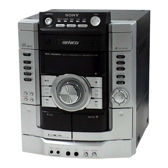
Photo: HCD-RG590 (Except AEP, UK, Russian models)
Model Name Using Similar Mechanism
CD Mechanism Type
CD
Section
Base Unit Name
Optical Pick-up Block Name
TAPE
Model Name Using Similar Mechanism
Section
Tape Transport Mechanism Type
SPECIFICATIONS
Subwoofer
DIN power output (rated): 120 watts
(6 ohms at 80 Hz, DIN)
Continuous RMS power output
(reference): 150 watts (6 ohms at 80 Hz,
10% THD)
Music power output (reference):
300 watts (6 ohms at 80 Hz, 10% THD)
Other models:
HCD-RG590
The following are measured at AC 220 V, 50 Hz
(Argentine model), AC 120 or 127 V, 60 Hz
(Mexican model), AC 127 or 220 V, 60 Hz
(Saudi Arabian model), AC 120, 220 or 240 V,
50/60 Hz (other models)
Front speaker:
DIN power output (rated): 110 + 110 W
(6 ohms at 1 kHz, DIN)
Continuous RMS power output (reference):
145 + 145 W (6 ohms at 1 kHz, 10% THD)
HCD-RG270
CDM74KF-K6BD83S (Except Mexican model)/
CDM74KF-F1BD84 (Mexican model)
BU-K6BD83S-WOD (Except Mexican model)/
BU-F1BD84 (Mexican model)
KSM-213DCP (Except Mexican model)/
KSM-215DCP (Mexican model)
NEW
CWN42FF609
Subwoofer:
DIN power output (rated): 130 W
(6 ohms at 80 Hz, DIN)
Continuous RMS power output (reference):
170 W (6 ohms at 80 Hz, 10% THD)
HCD-RG490
Front speaker
The following are measured at AC 120, 127,
220, 240 V 50/60 Hz
DIN power output (rated): 95 + 95 watts
(6 ohms at 1 kHz, DIN)
Continuous RMS power output
(reference): 125 + 125 watts (6 ohms at
1 kHz, 10% THD)
Subwoofer
DIN power output (rated): 120 watts
(6 ohms at 80 Hz, DIN)
Continuous RMS power output
(reference): 150 watts (6 ohms at 80 Hz,
10% THD)
COMPACT DISC DECK RECEIVER
AEP Model
E Model
HCD-RG490/RG590
UK Model
HCD-RG590
Australian Model
HCD-RG490
– Continued on next page –
Advertisement
Chapters
Table of Contents

Related Manuals for Sony HCD-RG590


Summarization of Contents
SPECIFICATIONS
Amplifier and Output Specifications
Details power output for amplifier, subwoofer, front speakers across models.
GENERAL INFORMATION
Unit Inputs, Outputs, and Section Specs
Describes unit connections, CD, tape, tuner, and general unit specs.
DISASSEMBLY PROCEDURES
Step-by-Step Disassembly Flow
Outlines the sequence for disassembling the unit and its main boards.
Case and Lid Removal
Details the removal of side, top, and CD lid parts.
Board and Mechanism Disassembly
Details removal of main boards, CD mechanism, optical pick-up, and motors.
TEST MODE OPERATIONS
System Modes and Diagnostic Procedures
Details cold reset, CD ship, anti-theft, amplifier, and MC test modes.
MECHANICAL ADJUSTMENTS
Precautions and Measurement Procedures
Guidelines for adjustments, cleaning, torque, and tape tension measurements.
ELECTRICAL ADJUSTMENTS
Head Azimuth Adjustment Procedure
Procedure for record/playback head azimuth adjustment and related precautions.
CIRCUIT DIAGRAMS
Block Diagrams Overview
Illustrates functional blocks for CD servo, main, AMP/VIDEO, and panel/power supply sections.
Diagram and PCB Conventions
Explains symbols, notations, and component markings used in diagrams and PCBs.
EXPLODED VIEWS
Unit and Component Disassembly Views
Exploded views showing the disassembly of the unit's case, boards, and mechanisms.
TEST MODE OPERATIONS
System Modes and Diagnostic Procedures
Details cold reset, CD ship, anti-theft, and various test modes for diagnosis.
VERSION AND ERROR CODE DISPLAY
Error Code Interpretation
Explains the meaning of different digits in mechanism deck and optical pick-up error codes.
MECHANICAL ADJUSTMENTS
Adjustment Precautions and Measurement Specifications
Guides on cleaning, torque, and tape tension measurements for mechanical adjustments.
ELECTRICAL ADJUSTMENTS
Head Azimuth Adjustment Procedure
Procedure for record/playback head azimuth adjustment and related precautions.
CD SECTION OPERATIONS
Focus Bias Check Procedure
Steps for checking focus bias and evaluating the eye pattern waveform.
CIRCUIT DIAGRAMS
Block Diagrams Overview
Illustrates the functional blocks for CD servo, main, AMP/VIDEO, and panel/power supply sections.
Diagram and PCB Conventions
Explains symbols, notations, and component markings used in diagrams and PCBs.
NOTES ON CIRCUIT DIAGRAMS AND BOARDS
Diagram and PCB Conventions
Explains symbols, notations, and component markings used in diagrams and PCBs.
PRINTED WIRING BOARD – CD Board
CD Board Layouts
Visual layout of components on the component and conductor sides of the CD board.
SCHEMATIC DIAGRAM – CD Board
CD Board Schematic Details
Detailed schematic of the CD board, showing ICs and their connections.
PRINTED WIRING BOARD – BD Board
BD Board Layouts
Visual layout of components on the component and conductor sides of the BD board.
SCHEMATIC DIAGRAM – BD Board
BD Board Schematic Details
Detailed schematic of the BD board, showing ICs and their connections.
PRINTED WIRING BOARDS – CHANGER Section
Changer Section Board Layouts
Visual layout of components on the driver, motor, sensor, and SW boards.
SCHEMATIC DIAGRAM – CHANGER Section
Changer Section Schematic
Schematic diagram of the changer section, detailing driver, motor, sensor, and SW board connections.
PRINTED WIRING BOARD – DECK Board
DECK Board Layouts
Visual layout of components on the component and conductor sides of the DECK board.
SCHEMATIC DIAGRAM – DECK Board
DECK Board Schematic
Detailed schematic of the DECK board, showing ICs and component connections.
PRINTED WIRING BOARD – MAIN Board (Except MX)
MAIN Board Layout (Except MX)
Visual layout of components on the component side of the MAIN board.
SCHEMATIC DIAGRAM – MAIN Board (1/3) (Except MX)
MAIN Board Schematic (1/3) (Except MX)
Schematic of the MAIN board, detailing system controller and related circuits.
SCHEMATIC DIAGRAM – MAIN Board (2/3) (Except MX)
MAIN Board Schematic (2/3) (Except MX)
Schematic of the MAIN board, showing equalizer and input selector circuits.
SCHEMATIC DIAGRAM – MAIN Board (3/3) (Except MX)
MAIN Board Schematic (3/3) (Except MX)
Schematic of the MAIN board, detailing power supply and output circuits.
PRINTED WIRING BOARD – MAIN Board (RG490/RG590 MX)
MAIN Board Layout (RG490/RG590 MX)
Visual layout of components on the component side of the MAIN board for MX models.
SCHEMATIC DIAGRAM – MAIN Board (1/3) (RG490/RG590 MX)
MAIN Board Schematic (1/3) (RG490/RG590 MX)
Schematic of the MAIN board for MX models, detailing system controller and related circuits.
SCHEMATIC DIAGRAM – MAIN Board (2/3) (RG490/RG590 MX)
MAIN Board Schematic (2/3) (RG490/RG590 MX)
Schematic of the MAIN board for MX models, showing equalizer and input selector circuits.
SCHEMATIC DIAGRAM – MAIN Board (3/3) (RG490/RG590 MX)
MAIN Board Schematic (3/3) (RG490/RG590 MX)
Schematic of the MAIN board for MX models, detailing power supply and output circuits.
PRINTED WIRING BOARD – MIC. AUX. HP Board
MIC. AUX. HP Board Layout
Visual layout of components on the MIC. AUX. HP board.
SCHEMATIC DIAGRAM – MIC. AUX. HP Board
MIC. AUX. HP Board Schematic
Schematic diagram for the MIC. AUX. HP board, detailing ICs and component connections.
PRINTED WIRING BOARD – POWER Board (RG490)
POWER Board (RG490) Layout
Visual layout of components on the POWER board for RG490.
SCHEMATIC DIAGRAM – POWER Board (RG490)
POWER Board (RG490) Schematic
Schematic diagram for the POWER board (RG490), showing amplifier and power supply circuits.
PRINTED WIRING BOARD – POWER Board (RG590)
POWER Board (RG590) Layout
Visual layout of components on the POWER board for RG590.
SCHEMATIC DIAGRAM – POWER Board (RG590)
POWER Board (RG590) Schematic
Schematic diagram for the POWER board (RG590), showing amplifier and power supply circuits.
PRINTED WIRING BOARDS – SUB WOOFER Section
SUB WOOFER Section Layouts
Visual layout of components on the SUB WOOFER and SW-SP boards.
SCHEMATIC DIAGRAM – SUB WOOFER Section
SUB WOOFER Section Schematic
Schematic diagram for the SUB WOOFER section, detailing IC and component connections.
PRINTED WIRING BOARDS – CD-G Section (RG490/RG590 MX)
CD-G Board Layouts
Visual layout of components on both sides of the CD-G board.
SCHEMATIC DIAGRAM – CD-G Section (RG490/RG590 MX)
CD-G Section Schematic
Schematic diagram of the CD-G section, showing ICs and connections to video out.
PRINTED WIRING BOARD – PANEL Board
PANEL Board Layout
Visual layout of components on the PANEL board, including key sections.
PRINTED WIRING BOARDS – KEY Section (Except MX)
KEY Section Layouts (Except MX)
Visual layouts for KEY TOP, KEY LEFT, and KEY RIGHT boards (non-MX models).
SCHEMATIC DIAGRAM – PANEL/KEY Section (Except MX)
PANEL/KEY Section Schematic (Except MX)
Schematic diagram for the PANEL and KEY sections (non-MX models), showing button connections.
Waveforms
Waveform Examples
Oscilloscope waveforms for various ICs and components across CD, BD, DECK, CD-G, and PANEL boards.
PRINTED WIRING BOARD – TRANSFORMER Board (RG490)
Transformer Board (RG490) Layout
Visual layout of components on the transformer board for RG490.
SCHEMATIC DIAGRAM – TRANSFORMER Board (RG490)
Transformer Board (RG490) Schematic
Schematic diagram for the transformer board (RG490), showing power supply connections.
PRINTED WIRING BOARD – TRANSFORMER Board (RG590)
Transformer Board (RG590) Layout
Visual layout of components on the transformer board for RG590.
SCHEMATIC DIAGRAM – TRANSFORMER Board (RG590)
Transformer Board (RG590) Schematic
Schematic diagram for the transformer board (RG590), showing power supply connections.
IC Block Diagrams
CD and BD Board IC Block Diagrams
Block diagrams illustrating the internal structure of key ICs on the CD and BD boards.
IC Pin Function Description - CD Board IC201
CD Board IC201 Pin Details
Detailed pinout and function description for IC201 (CXD3014A-201R) on the CD board.
IC Pin Function Descriptions
MAIN Board IC101 Pin Functions and DRIVER Board ICs
Pin details for MAIN board IC101 and block diagrams for DRIVER board ICs.
IC Pin Function Descriptions
MAIN, MIC/HP, CD-G Board ICs
Pin details for MAIN board IC102, MIC/HP board IC802, and CD-G board IC block diagrams.
IC Pin Function Description - CD Board IC201 (Continued)
CD Board IC201 Pin Details (Continued)
Continuation of pinout and function description for IC201 on the CD board.
IC Pin Function Description - CD Board IC201 (Continued)
CD Board IC201 Pin Details (Continued)
Continuation of pinout and function description for IC201 on the CD board.
IC Pin Function Description - CD Board IC201 (Continued)
CD Board IC201 Pin Details (Continued)
Continuation of pinout and function description for IC201 on the CD board.
BD BOARD IC101 CXD3059AR (CD DSP) Pin Function Description
BD Board IC101 Pin Details
Detailed pinout and function description for IC101 (CXD3059AR) on the BD board.
MAIN BOARD IC901 uPD78F0547GC (S)-UBT-A (SYSTEM CONTROLLER) Pin Function Description
MAIN Board IC901 Pin Details
Detailed pinout and function description for IC901 on the MAIN board.
MAIN BOARD IC901 Pin Function Description (Continued)
MAIN Board IC901 Pin Details (Continued)
Continuation of pinout and function description for IC901 on the MAIN board.
MAIN BOARD IC901 Pin Function Description (Continued)
MAIN Board IC901 Pin Details (Continued)
Continuation of pinout and function description for IC901 on the MAIN board.
MAIN BOARD IC901 Pin Function Description (Continued)
MAIN Board IC901 Pin Details (Continued)
Continuation of pinout and function description for IC901 on the MAIN board.
MAIN BOARD IC901 Pin Function Description (Continued)
MAIN Board IC901 Pin Details (Continued)
Continuation of pinout and function description for IC901 on the MAIN board.
CD-G BOARD IC1001 TC9411AFG (BS, K) (CD GRAPHICS DECODER) Pin Function Description
CD-G Board IC1001 Pin Details
Detailed pinout and function description for IC1001 on the CD-G board.
PANEL BOARD IC701 uPD780232GC-509-8BT-A Pin Function Description
PANEL Board IC701 Pin Details
Detailed pinout and function description for IC701 on the PANEL board.
8-1. CASE SECTION
Case Section Exploded View
Exploded view showing the parts and assembly of the unit's case.
8-2. PANEL BOARD SECTION
Panel Board Exploded View
Exploded view showing the parts and assembly of the panel board.
8-3. LID (TOP) SECTION
Lid (Top) Section Exploded View
Exploded view illustrating the parts and assembly of the unit's top lid.
8-4. FRONT PANEL SECTION
Front Panel Section Exploded View
Exploded view showing the parts and assembly of the front panel section.
8-5. MAIN BOARD SECTION
Main Board Section Exploded View
Exploded view showing the main board and its associated parts.
8-6. POWER BOARD, SUB WOOFER BOARD SECTION
Power and Sub Woofer Board Exploded Views
Exploded views of the power board and subwoofer board assemblies.
8-7. CHASSIS SECTION
Chassis Section Exploded Views
Exploded views illustrating the chassis and transformer board components.
8-8. CD MECHANISM DECK SECTION-1
CD Mechanism Deck Section-1 Exploded View
Exploded view of the CD mechanism deck, showing parts like motors and gears.
8-9. CD MECHANISM DECK SECTION-2
CD Mechanism Deck Section-2 Exploded View
Exploded view of the CD mechanism deck section 2, showing optical pick-up and other components.
3. ELECTRICAL PARTS LIST
BD Board Components
List of electrical parts for the BD board, including capacitors, connectors, and ICs.
ELECTRICAL PARTS LIST
MAIN Board Components
List of electrical parts for the MAIN board, including transistors, resistors, and capacitors.
ELECTRICAL PARTS LIST
DECK Board Components
List of electrical parts for the DECK board, including capacitors, connectors, ICs, transistors, and resistors.
ELECTRICAL PARTS LIST
DRIVER Board Components
List of electrical parts for the DRIVER board, including capacitors, ICs, transistors, and resistors.
ELECTRICAL PARTS LIST
DECK Board Components (Continued)
Continuation of the DECK board parts list, detailing resistors and transistors.
ELECTRICAL PARTS LIST
DRIVER Board Components (Continued)
Continuation of the DRIVER board parts list, detailing resistors and switches.
ELECTRICAL PARTS LIST
KEY Components
List of electrical parts for the KEY LEFT and KEY RIGHT boards, including resistors and switches.
ELECTRICAL PARTS LIST
MAIN Board Components (RG490/RG590)
List of electrical parts for the MAIN board, detailing capacitors and connectors.
ELECTRICAL PARTS LIST
MAIN Board Components (Continued)
Continuation of the MAIN board parts list, including diodes, ICs, transistors, and jumpers.
ELECTRICAL PARTS LIST
MAIN Board Components (Continued)
Continuation of the MAIN board parts list, detailing transistors and resistors.
ELECTRICAL PARTS LIST
MAIN Board Components (Continued)
Continuation of the MAIN board parts list, detailing resistors.
ELECTRICAL PARTS LIST
MAIN Board Components (Continued)
Continuation of the MAIN board parts list, detailing resistors.
ELECTRICAL PARTS LIST
MIC. AUX. HP Board Components
List of electrical parts for the MIC. AUX. HP board, including capacitors, diodes, ICs, transistors, resistors, and switches.
ELECTRICAL PARTS LIST
MIC. AUX. HP Board Components (Continued)
Continuation of the MIC. AUX. HP board parts list, detailing resistors, variable resistors, and connectors.
ELECTRICAL PARTS LIST
MIC. AUX. HP Board Components (Continued)
Continuation of the MIC. AUX. HP board parts list, detailing capacitors, diodes and ICs.
ELECTRICAL PARTS LIST
DRIVER Board Components
List of electrical parts for the DRIVER board, including transistors, resistors, and capacitors.
ELECTRICAL PARTS LIST
MAIN Board Components (RG490/RG590)
List of electrical parts for the MAIN board, detailing capacitors and connectors.
ELECTRICAL PARTS LIST
POWER Board Components
List of electrical parts for the POWER board, detailing capacitors, connectors, diodes, ICs, transistors, and resistors.
ELECTRICAL PARTS LIST
SUB WOOFER Board Components
List of electrical parts for the SUB WOOFER board, including resistors, relays, connectors and capacitors.
ELECTRICAL PARTS LIST
TRANSFORMER Board Components
List of electrical parts for the TRANSFORMER board, detailing diodes, ICs, jumpers, transistors, resistors, and capacitors.
ELECTRICAL PARTS LIST
TRANSFORMER Board Components (Continued)
Continuation of the TRANSFORMER board parts list, including fuses and miscellaneous items.
SUPPLEMENT-1
DECK Board Component Change Information
Details changes in the DECK board (Component Side) from former to new type.
2. DIAGRAMS
Diagram and PCB Conventions
Explains symbols, notations, and component markings used in diagrams and PCBs.
2-1. PRINTED WIRING BOARD – DECK Board –
DECK Board Layout
Visual layout of components on the DECK board.
2-2. SCHEMATIC DIAGRAM – DECK Board –
DECK Board Schematic
Schematic diagram for the DECK board, showing component connections and ICs.
3. ELECTRICAL PARTS LIST
DECK Board Components
List of electrical parts for the DECK board, including capacitors, connectors, diodes, ICs, jumpers, transistors, and resistors.
ELECTRICAL PARTS LIST
DECK Board Components (Continued)
Continuation of the DECK board parts list, detailing resistors and transistors.
SUPPLEMENT-2
New/Former Description - MAIN, KEY Boards
Details changes in MAIN, KEY RIGHT, and KEY TOP boards from former to new types.
2. DIAGRAMS
Diagram and PCB Conventions
Explains symbols, notations, and component markings used in diagrams and PCBs.
2-1. PRINTED WIRING BOARD – MAIN Board (Except MX)
MAIN Board Layout (Except MX)
Visual layout of components on the component side of the MAIN board.
2-2. SCHEMATIC DIAGRAM – MAIN Board (1/3) (Except MX)
MAIN Board Schematic (1/3) (Except MX)
Schematic of the MAIN board, detailing system controller and related circuits.
2-3. SCHEMATIC DIAGRAM – MAIN Board (2/3) (Except MX)
MAIN Board Schematic (2/3) (Except MX)
Schematic of the MAIN board, showing equalizer and input selector circuits.
2-4. SCHEMATIC DIAGRAM – MAIN Board (3/3) (Except MX)
MAIN Board Schematic (3/3) (Except MX)
Schematic of the MAIN board, detailing power supply and output circuits.
2-5. PRINTED WIRING BOARD – MAIN Board (RG490/RG590 MX)
MAIN Board Layout (RG490/RG590 MX)
Visual layout of components on the component side of the MAIN board for MX models.
2-6. SCHEMATIC DIAGRAM – MAIN Board (1/3) (RG490/RG590 MX)
MAIN Board Schematic (1/3) (RG490/RG590 MX)
Schematic of the MAIN board for MX models, detailing system controller and related circuits.
2-7. SCHEMATIC DIAGRAM – MAIN Board (2/3) (RG490/RG590 MX)
MAIN Board Schematic (2/3) (RG490/RG590 MX)
Schematic of the MAIN board for MX models, showing equalizer and input selector circuits.
2-8. SCHEMATIC DIAGRAM – MAIN Board (3/3) (RG490/RG590 MX)
MAIN Board Schematic (3/3) (RG490/RG590 MX)
Schematic of the MAIN board for MX models, detailing power supply and output circuits.
2-9. PRINTED WIRING BOARDS – KEY Section (Except MX)
KEY Section Layouts (Except MX)
Visual layouts for KEY TOP, KEY LEFT, and KEY RIGHT boards (non-MX models).
2-10. SCHEMATIC DIAGRAM – KEY Section (Except MX)
KEY Section Schematic (Except MX)
Schematic diagram for the KEY section (non-MX models), showing button connections.
2-11. PRINTED WIRING BOARDS – KEY Section (RG490/RG590 MX)
KEY Section Layouts (RG490/RG590 MX)
Visual layouts for KEY TOP, KEY LEFT, and KEY RIGHT boards (MX models).
2-12. SCHEMATIC DIAGRAM – KEY Section (RG490/RG590 MX)
KEY Section Schematic (RG490/RG590 MX)
Schematic diagram for the KEY section (MX models), showing button and encoder connections.
3. ELECTRICAL PARTS LIST
KEY Components
List of electrical parts for the KEY LEFT and KEY RIGHT boards, including resistors and switches.
ELECTRICAL PARTS LIST
MAIN Board Components
List of electrical parts for the MAIN board, detailing capacitors and resistors.
ELECTRICAL PARTS LIST
MAIN Board Components (Continued)
Continuation of the MAIN board parts list, including diodes, ICs, transistors, and jumpers.
ELECTRICAL PARTS LIST
MAIN Board Components (Continued)
Continuation of the MAIN board parts list, detailing transistors and resistors.
ELECTRICAL PARTS LIST
MAIN Board Components (Continued)
Continuation of the MAIN board parts list, detailing resistors.
ELECTRICAL PARTS LIST
MAIN Board Components (Continued)
Continuation of the MAIN board parts list, detailing resistors.
ELECTRICAL PARTS LIST
MAIN Board Components (Continued)
Continuation of the MAIN board parts list, detailing resistors and vibrators.
REVISION HISTORY
Revision Details
Lists the versions and changes made to the service manual over time.
Need help?
Do you have a question about the HCD-RG590 and is the answer not in the manual?
Questions and answers