Table of Contents
Advertisement
Quick Links
SERVICE MANUAL
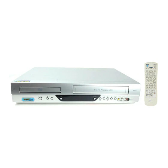
Product Type: VCR+DVD COMBI
Chassis: D37 + DP-10C
Manual Series: XBV613
Manual Part #: 3829RGN005G
Model Line: D
Product Year: 2006
CONTENTS
SUMMARY
................................................
CABINET & MAIN CHASSIS
ELECTRICAL
............................................
MECHANISM OF VCR PART
REPLACEMENT PARTS LIST
Published March 2006
by Technical Publications
Zenith Electronics Corporation
201 James Record Road
Huntsville, Alabama 35824-1513
Copyright © 2006 by Zenith Electronics Corporation
Printed in U.S.A
Model Series:
XBV613
1
....................
2
3
...................
4
..................
5
Advertisement
Chapters
Table of Contents
Troubleshooting

Subscribe to Our Youtube Channel
Related Manuals for Zenith XBV613 - DVD/VCR Combination


Summary of Contents for Zenith XBV613 - DVD/VCR Combination
- Page 1 CABINET & MAIN CHASSIS ....ELECTRICAL ..........MECHANISM OF VCR PART ....REPLACEMENT PARTS LIST ....Published March 2006 by Technical Publications Zenith Electronics Corporation 201 James Record Road Huntsville, Alabama 35824-1513 Copyright © 2006 by Zenith Electronics Corporation Printed in U.S.A...
- Page 2 CONTENTS SECTION 1 ..SUMMARY SECTION 2 ..CABINET & MAIN CHASSIS SECTION 3 ..ELECTRICAL SECTION 4 ..MECHANISM OF VCR PART SECTION 5 ..REPLACEMENT PARTS LIST...
-
Page 3: Table Of Contents
SECTION 1 SUMMARY CONTENTS PRODUCT SAFETY SERVICING GUIDELINES FOR VIDEO PRODUCTS ..... 1-3 SERVICING PRECAUTIONS ....................1-4 • General Servicing Precautions • Insulation Checking Prodedure • Electrostatically Sensitive Devices SERVICE INFORMATION FOR EEPROM ................1-5 SPECIFICATIONS ........................1-6... -
Page 4: Product Safety Servicing Guidelines For Video Products
PRODUCT SAFETY SERVICING GUIDELINES FOR VIDEO PRODUCTS CAUTION : DO NOT ATTEMPT TO MODIFY THIS PRODUCT IN ANY WAY, SUBJECT : X-RADIATION NEVER PERFORM CUSTOMIZED INSTALLATIONS WITHOUT MANUFAC- 1. BE SURE PROCEDURES AND INSTRUCTIONS TO ALL SERVICE PER- TURER’S APPROVAL. UNAUTHORIZED MODIFICATIONS WILL NOT ONLY SONNEL COVER THE SUBJECT OF X-RADIATION. -
Page 5: Servicing Precautions
SERVICING PRECAUTIONS CAUTION : Before servicing the VCR+DVD covered by this Electrostatically Sensitive (ES) Devices service data and its supplements and addends, read and fol- Some semiconductor (solid state) devices can be damaged low the SAFETY PRECAUTIONS. NOTE : if unforeseen cir- easily by static electricity. -
Page 6: Service Information For Eeprom
SERVICE INFORMATION FOR EEPROM POWER ON DETECT NEW EEPROM DVD LOGO Status (NO Disk status) (OPTION EDIT SCREEN) MODEL XBV613 NAME HEX Remotecontrol OPT 1 55 Pause key-->1-->4-->7-->2 in order. OPT 2 53 OPT 3 00 OPT 4 45 OPT 5 12 Press number 0~9, Press charater OPT 6 05 A~F (1~6 for a while) -
Page 7: Specifications
SPECIFICATIONS • GENERAL Power requirements 120V, 60Hz Power consumption 16 W Dimensions (approx.) 430 x 78.5 x 265 mm (W x H x D) Mass (approx.) 4.2 kg Operating temperature 5˚C to 40˚C (41˚F to 104˚F) Operating humidity 5 % to 90 % Signal system NTSC •... - Page 8 SECTION 2 CABINET & MAIN CHASSIS CONTENTS EXPLODED VIEWS ........................2-2 1. Cabinet and Main Frame Section ...................2-2 2. DECK MECHANISM SECTION [ DVD MD (DP-10C) ] ............2-3 3. Packing Accessory Section ....................2-4...
-
Page 9: Exploded Views
EXPLODED VIEWS 1. CABINET AND MAIN FRAME SECATION NOTES) THE EXCLAMATION POINT WITHIN AN EQUILATERAL TRIANGLE IS INTENDED TO ALERT THE SERVICE PERSONNEL TO THE PRESENCE OF IMPORTANT SAFETY INFORMATION IN SERVICE LITERATURE. -
Page 10: Deck Mechanism Section [ Dvd Md (Dp-10C) ]
2. DECK MECHANISM SECTION [ DVD MD (DP-10C) ] 015B 015A 012A 012A... -
Page 11: Packing Accessory Section
3. PACKING ACCESSORY SECTION 810 CABLE ASS'Y RF RF CABLE PLUG ASS'Y 1WAY BATTERY PLUG ASS'Y 2WAY REMOTE CONTROLLER ASSEMBLY INSTRUCTION ASSEMBLY PACKING, CASING PACKING, CASING... - Page 12 SECTION 3 ELECTRICAL CONTENTS VCR PART DVD PART ELECTRICAL ELECTRICAL ADJUSTMENT TROUBLESHOOTING GUIDE ......3-57 PROCEDURES ............3-2 1. POWER CHECK FLOW ........3-57 2. SYSTEM OPERATION FLOW......3-58 ELECTRICAL 3. TEST & DEBUG FLOW ........3-59 TROUBLESHOOTING GUIDE ......3-3 1. POWER(SMPS) CIRCUIT........3-3 DETAILS AND WAVEFORMS ON SYSTEM 2.
-
Page 13: Servo Adjustment
VCR PART ELECTRICAL ADJUSTMENT PROCEDURES 1. Servo Adjustment 1) PG Adjustment • Test Equipment a) OSCILLOSCOPE b) NTSC MODEL : NTSC SP TEST TAPE • Adjustment And Specification MODE MEASUREMENT POINT ADJUSTMENT POINT SPECIFICATION V.Out PLAY R/C TRK JIG KEY 6.5 ±... -
Page 14: Electrical Troubleshooting Guide
ELECTRICAL TROUBLESHOOTING GUIDE 1. Power(SMPS) CIRCUIT (1) No 5.3VA No 5.3VA Is the FR101 Replace FR101 Normal? (Use the same ICW) Is BD101 Normal? Replace BD101 Is R101 Normal? Replace R101 Is Vcc (9V - 18V) sup- Check or Replace Is D102 normal? plied to IC101 Pin2? D102... - Page 15 (2) No 5.0V_D (3) No 5.0V_T No 5.0V_D No 5.0V_T Is the Vcc(5.3V) sup- Is the Vcc(5.3V) sup- Check or Replace Check or Replace plied to Q165 Emittor? D125 D125 plied to Q163 Emittor? Is the Q162 Base Is the Q162 Base Check the PWR CTL Check the PWR CTL ‘H’?
- Page 16 (6) No Motor_Vcc (To Cap, Drum Motor ) (7) No REG 12V No Motor_Vcc No REG 12V Check or Replace Check or Replace Is the Vcc(14V) Is the Vcc(14V) supplied supplied to C134? to Q165 Collector? D124 D124 Is the Vcc(14V) sup- Check or Replace Check the PWR CTL the Cap / Drum...
-
Page 17: System/Key Circuit
2. SYSTEM/KEY CIRCUIT (1) AUTO STOP Auto Stop Check the Drum Motor Does the SW30 waveform appear at IC501 Pin18? signal. Do T/UP Reel Pulses Do the T-UP Reel Pulses appear at the point Does 5V appear at RS501? appear at IC501 Pin80? between R556 and R536? Replace the T/UP Reel Check the Q165 Power... -
Page 18: Servo Circuit
3. SERVO CIRCUIT (1) Unstable Video in PB MODE Unstable Video in PB Mode. Does the Noise level of the screen change periodically? Do the CTL pulses appear Is adjusting the height of at IC501 Pin97? the CTL Head accurate? Readjust the height of the Does the CFG waveform CTL Head. - Page 19 2. SERVO CIRCUIT (3) When the Capstan Motor doesn’t run, When the Capstan Motor doesn’t run, Refer to “SMPS(CAPSTAN/12Volt) Does 12VA appear at PMC01? Trouble Shooting”. Does 2.8V appear at PMC01 Pin 9? Check the PMC01 and the Capstan Does the PWM signal appear at IC501 Pin77? Motor Ass’y.
-
Page 20: Osd Circuit
2. SERVO CIRCUIT (4) KEY doesn’t working KEY doesn’t working. Is 5V applied to IC501 Refer to “SMPS 5.3VA Pin99? Trouble Shooting”. Does LED or FLD change Replace the defective when a function button is switches. pressed? 4. OSD CIRCUIT (1) No OSD display. -
Page 21: Y/C Circuit
5. Y/C CIRCUIT (1) No Video in EE Mode, No Video in EE Mode Does the Video signal Does the Video signal Check DVD Video Input appear at IC301 Pins28, appear at IC302 Pins1, (IC601, Pin150), Tuner 30, 32? Video Input (TU701 Pin16), Line Video Input (JK901), respectively. - Page 22 3. Y/C CIRCUIT (2) When the Y(Luminance) signal doesn’t appear on the screen in PB Mode, Is 5V applied to IC301 Check the line of the SW 5V Line. Pins23, 44, 45, 52, 68, 77? Is the Y/C Bus siganl Refer to ‘SYSTEM Y/C applied to IC301 Pins53, BUS CHECK Trouble...
- Page 23 3. Y/C CIRCUIT (3) When the C(Color) signal doesn’t appear on the screen in PB Mode, Is SW 5V applied to IC301 Check the line of the REG 5V Line. (Power Circuit) Pins23, 44, 45, 52, 68, 77? Does the Color signal Is the oscillation frequency appear at IC301 Pins41, Replace X301.
- Page 24 3. Y/C CIRCUIT (4) When the Video signal doesn’t appear on the screen in REC Mode, REC mode Is EE mode normal? Check the EE mode Is brightness normal? Is color normal? Is the brightness signal sup- Does signal appear at Check X301 oscillation IC301 Pins41, 50? frequency.
-
Page 25: Hi-Fi Circuit
6. Hi-Fi CIRCUIT (1) No Sound(EE Mode) No Sound. Check the SIF.IN of IC801 Pins57. Check the TU701 SIF Pin13. Check the DVD Audio of IC801 Check the DVD MODULE. (PMD02 Pins13, 15). Pins12, 74. Check the LINE1 Audio of IC801 Check the Rear Jack. - Page 26 3. Y/C CIRCUIT (2) Hi-Fi Playback PB mode No Sound. Check the Vcc of IC801 Check Power. (Pins3, 5, 15, 32, 36, 46, 54). Check the Hi-Fi Selection switch. Check IC501 Pin19 (A.H/SW) (IC801 Pin39) and the Tape quality. Is the RF Envelope at IC801 Pin23 over 3Vp-p? Check IC801 Pin37(Data), Check the parts of µ-COM...
- Page 27 (3) Hi-Fi REC Hi-Fi REC. It is impossible to record Hi-Fi Audio signal. Check Vcc of IC801. Check Power. (Pins3, 5, 15, 32, 36, 46, 54) Check ports of µ-CPM. Check IC801 Pin37(Data), Pin38(CLOCK). (IC501 Pins71, 72) Check Audio input signal of IC801 Do Audio signals appear at IC801 Pin6? Pin57(TU.A.), 7, 69(DVD.A.), 11, 73(LINE1.A.), 9, 71(LINE2.A.)
-
Page 28: Tuner/If Circuit
7. Tuner/IF CIRCUIT (1) No Picture on the TV screen No picture on the TV screen Does the Video signal at Is +33V applied to TU701 Check 33V line. the TU701 Pin16. Pin14? Is +5V applied to TU701 Check 5V line. Pin3? Does the Clock signal Check the lIC Clock Signal... - Page 29 (2) No Sound No Sound. Check the Vcc of TU701 Pins3, 14. Check 5V, 33V Line. Check the Tuner SiF signal at IC801 Check the Tuner SIF of TU701 Pin13. Pin57. 1. Check the Vcc(5.3VA, 9V) of IC801 Check the Audio of IC801 Pins78, 80. Pins3, 5, 36, 54.
-
Page 30: Block Diagrams
BLOCK DIAGRAMS 1. POWER(SMPS) BLOCK DIAGRAM T101 TRANS BD101 RECTIFIER & SNUBBER MOTOR VCC SMOOTING BLOCK C103 BLOCK 14VA 12V REG BLOCK (D124,C124,C134, (D101,C105 (Q166,ZD151,C160, R133,L124,C126) REG12V C106,R104) R166,C159) 9V REG BLOCK REG9V (Q164,ZD152,C161, R168,C166) DRIVE & S/W BLOCK (IC101, D102, R105, 8V REG BLOCK NOISE FILTER C104, C108 , C109,... -
Page 31: Tu/If Block Diagram
2. TU/IF BLOCK DIAGRAM 875 MOD A.IN MOD CTL 107 5V VCR 'H' 971 MOD VEDIO TU.V.OUT IIC CLK IIC DATA 781 SIF OUT COMBI NTSC 3-21 3-22... -
Page 32: Y/C Block Diagram
3. Y/C BLOCK DIAGRAM (PB Mode) (REC Mode) 55 54 53 51 50 49 48 47 55 54 53 AUDIO C-ROT 320FH SERIAL VX01 MUTE RF-SW DECODER HA SW CLAMP CLAMP EP PB 'A' EP REC CLAMP EP PB 'B' CLAMP IC302 3.58M... -
Page 33: Normal Audio Block Diagram
4. NORMAL AUDIO BLOCK DIAGRAM (EE Mode) (PB Mode) (REC Mode) 3-25 3-26... -
Page 34: Hi-Fi Block Diagram
5. Hi-Fi BLOCK DIAGRAM Hi-Fi/ AUDIO INPUT 26 27 BLOCK DEMO DULATE FM MODU A.OUT 'L' DE MODU DVD A.IN 'L' A.OUT DVD AUDIO To JACK A.OUT 'R' DVD A.IN 'R' AV1 A.IN 'L' INPUT REAR JACK OUTPUT AV1 A.IN 'R' SELECT SELECT MODULATOR... -
Page 35: System Block Diagram
6. SYSTEM BLOCK DIAGRAM TO/FROM DECK TO/FROM DECK TO/FROM AVCP TO/FROM AVCP 5.3VA MODE S/W MS501 9 18 95 94 87 12 13 16 59 CV IN I-Limit COMP IN MODE S1 MODE S1 MODE S2 REC 'H' MODE S2 MODE S3 MODE S4 C.ROT... -
Page 36: Circuit Diagrams
CIRCUIT DIAGRAMS IMPORTANT SAFETY NOTICE CUIT. SPECIAL COMPONENTS ARE SHADED ON THE NOTE : SCHEMATIC FOR EASY IDENTIFICATION. 1. Shaded( ) parts are critical for safety. Replace only WHEN SERVICING THIS CHASSIS, UNDER NO CIR- THIS CIRCUIT DIAGRAM MAY OCCASIONALLY DIF- with specified part number. -
Page 37: Tu/If Circuit Diagram
2. TU/IF CIRCUIT DIAGRAM 3-33 3-34... -
Page 38: A/V Circuit Diagram
3. A/V CIRCUIT DIAGRAM 3-35 3-36... -
Page 39: Hi-Fi Circuit Diagram
4. Hi-Fi CIRCUIT DIAGRAM 3-37 3-38... -
Page 40: Jack Circuit Diagram
5. JACK CIRCUIT DIAGRAM 3-39 3-40... -
Page 41: System Circuit Diagram
6. SYSTEM CIRCUIT DIAGRAM 3-41 3-42... -
Page 42: Waveforms
• WAVEFORMS * IC301 Waveform * IC501 Waveform Stop : 10.0KS/s 280 Acqs Stop : 250KS/s 299 Acqs Stop : 10.0KS/s 18 Acqs Trigger Position: 12% Stop : 10.0KS/s 27 Acqs 1.00 V M 5.00ms 3.04 V 1.00 V M5.00ms 3.04 V 1.00 V M 200µs... -
Page 43: Circuit Voltage Chart
• CIRCUIT VOLTAGE CHART MODE MODE MODE MODE MODE MODE MODE MODE MODE STOP PLAY STOP PLAY STOP PLAY STOP PLAY STOP PLAY STOP PLAY STOP PLAY STOP PLAY STOP PLAY PIN NO. PIN NO. PIN NO. PIN NO. PIN NO. PIN NO. - Page 44 MODE MODE MODE MODE MODE STOP PLAY STOP PLAY STOP PLAY STOP PLAY STOP PLAY PIN NO. PIN NO. PIN NO. PIN NO. PIN NO. 0.05 0.05 1.56 0.15 2.26 3.22 2.23 0.05 0.05 1.35 0.53 0.04 3.18 3.22 2.25 2.41 3.19 3.22...
-
Page 45: Printed Circuit Diagrams
PRINTED CIRCUIT DIAGRAMS 1. MAIN P.C.BOARD (TOP SIDE) 3-49 3-50... -
Page 46: Main P.c.board (Bottom Side)
2. MAIN P.C.BOARD (BOTTOM SIDE) 3-51 3-52... -
Page 47: Power P.c.board
3. POWER P.C.BOARD LOCATION GUIDE NOTES) Warning NOTES) Parts that are shaded are critical NOTES) With respect to risk of fire or NOTES) electricial shock. 3-53 3-54... -
Page 48: Key P.c.board
4. KEY P.C.BOARD 3-55 3-56... -
Page 50: Dvd Part
DVD PART ELECTRICAL TROUBLESHOOTING GUIDE 1. POWER CHECK FLOW No 5V No 3.4VA. Is 3.4VA section working? Is 3.4VA section working? Is 5.6V present at collector Is 3.4V present at emitter No 3.4VA of Q126? of Q121? Replace Q126. Check FR101 Replace Q121. -
Page 51: System Operation Flow
2. SYSTEM OPERATION FLOW Power On 1. 186 CPU initializes SERVO,DSP & RISC registers 2. Write RISC code to SDRAM 3. Reset RISC Show LOGO Tray Closed ? Tray Close to Closed position SLED at Inner Side ? SLED Moves to Inner Position 1. -
Page 52: Test & Debug Flow
3. Test & debug flow TEST Check the AC Voltage Replace power PCBA or AC transformer. Power PCBA(110V or 220V) Switch on the Power PCBA Is the DC Voltage outputs OK? Repair or Replace Power PCBA (5V, 3.3V, 12V, 5.6V MOTOR) Make sure the main PCBA don't short on VCCs and switch it on. - Page 53 RESET or Power On. Check connection lines between Flash Memory operates Show LOGO? FLASH & ZR336888 and the FLASH properly? access time whether is suitable or not. Check connection lines SDRAM works properly? between SDRAM & ZR36882 and the SDRAM is damaged. ZR36882 VIDEO outputs Check the related circuit of properly?
- Page 54 Does the SLED move to Motor Driver MUTE Pin is Check the connection line of inner side when it is at outter High? MUTE signal. position? Is SLED_S DC Level higher Check the related circuit of than 1.65V? FMSO. SLED+ and SLED- output Check the amp circuit on properly? motor driver.
- Page 55 Check the laser power circuit Laser turns on when LD_DVD or LD_CD on ZR36882 and connecting reading disc? output properly? to power transistor. Collector voltage of power Check the related circuit on transistor is OK? laser power transistor Check cable connection between transistor ouput and pick-up head.
- Page 56 Proper signals on A,B,C,D Check connections between Focus ON OK? of ZR36882 ZR36882 and pick-up head. Check the FOCUS_S Check FE signal on connection on ZR36882 ZR36882 and motor driver. Check FOCUS_S signal on ZR36882 Normal TE Signal on Check the related Track On OK? ZR36882? circuit on ZR36882...
- Page 57 Normal Audio output Audio DAC received Check connection between when disc playback? correct data stream? ZR36882 & Audio DAC. Check the related circuit of Normal Audio DAC out? Audio DAC. Check Audio filter, amplify, mute circuit. Communications between Normal IR.VFD & Front Check communication lines IR.VFD Front panel key &...
-
Page 58: Details And Waveforms On System Test And Debugging
DETAILS AND WAVEFORMS ON SYSTEM TEST AND DEBUGGING 1. SYSTEM 27MHz CLOCK, RESET SIGNAL 1) ZR36882 main clock is at 27MH(X601) 3.1V,27MHz FIG 1-1 2) ZR3682 reset is low active 3.3VA PWR_CTL RESET Reset Time FIG 1-2 3-65... -
Page 59: Sdram Clock
2. SDRAM CLOCK 1) SDRAM clock is at 143MHz CLK=143MHz,Vp-p=3.3V IC603 PIN38 FIG 2-1 3. TRAY OPEN/CLOSE SIGNAL 1) Tray open/close waveform OPEN CLOSE OPEN CLOSE FIG 3-1 3-66... - Page 60 2) Tray open waveform OPEN CLOSE FIG 3-2 3) Tray close waveform OPEN CLOSE FIG 3-3 3-67...
-
Page 61: Sled Control Related Signal(No Disc Condition)
4. SLED CONTROL RELATED SIGNAL(NO DISC CONDITION) SLED_S DRVSB SLED+ SLED- FIG 4-1 5. LENS CONTROL RELATED SIGNAL(NO DISC CONDITION) FOCUS_S FOCUS+ FOCUS- FIG 5-1 3-68... -
Page 62: Laser Power Control Related Signal(No Disc Condition)
6. LASER POWER CONTROL RELATED SIGNAL(NO DISC CONDITION) DCLK = 128MHz, Vp-p=2.2, Vmax=2.7V VR_CD DVD_LD CD_LD FIG 6-1 7. DISC TYPE JUDGEMENT WAVEFORM FACT+ SBAD FIG 7-1(DVD) 3-69... - Page 63 FACT+ SBAD FIG 7-2 (DVD) FACT+ SBAD FIG 7-3 (CD) 3-70...
-
Page 64: Focus On Waveform
FACT+ SBAD FIG 7-4 (CD) 8. FOCUS ON WAVEFORM FOSO FACT+ FACT- FIG 8-1 (DVD) 3-71... -
Page 65: Spindle Control Waveform(No Disc Condition)
FOCUS FACT+ FACT- FIG 8-2 (CD) 9. SPINDLE CONTROL WAVEFORM(NO DISC CONDITION) SPINDLE_S (DVD) FIG 9-1 3-72... -
Page 66: Tracking Control Related Signal(System Checking)
10. TRACKING CONTROL RELATED SIGNAL(System checking) TRACK_S TACT+ TACT- FIG 10-1 (DVD) TRACK_S TACT+ TACT- FIG 10-2 (CD) 3-73... -
Page 67: Rf Waveform
11. RF WAVEFORM FIG 11-1 12. ZR36882 AUDIO OPTICAL AND COAXIAL OUTPUT(SPDIF) SPDIF FIG 12-1 3-74... -
Page 68: Zr36882 Video Output Waveform
13. ZR36882 VIDEO OUTPUT WAVEFORM 1) Full colorbar signal(CVBS) JK702 pin6 FIG 13-1 2) Y JK702 pin7 FIG 13-2 3-75... -
Page 69: Audio Output From Audio Dac
3) C JK702 PIN8 FIG 13-3 14. AUDIO OUTPUT FROM AUDIO DAC 1) AUDIO L/R 1KHz 0DB JK702 PIN4,5 FIG 14-1 3-76... - Page 70 2) Audio Related Signal AOUT0 ABCK ALRCLK FIG 14-2 3-77...
-
Page 71: Block Diagrams
BLOCK DIAGRAMS 1. SYSTEM BLOCK DIAGRAM RAMDQM RAMDAT[00:15] FACT+/-,TACTT +/- MOT_SPDL +/- SLED+,SLED-- LOAD+/- DECK MECHANISM 3-78... -
Page 72: Servo Block Diagram
2. SERVO BLOCK DIAGRAM 3-79... -
Page 73: Audio & Video In/Out Block Diagram
3. AUDIO & VIDEO IN/OUT BLOCK DIAGRAM DVD_A_L DVD_A_R 3-80... -
Page 74: Circuit Diagrams
CIRCUIT DIAGRAMS 1. SYSTEM CIRCUIT DIAGRAM 3-81 3-82... -
Page 75: Servo Circuit Diagram
2. SERVO CIRCUIT DIAGRAM 3-83 3-84... -
Page 76: Av/Jack Circuit Diagram
3. AV/JACK CIRCUIT DIAGRAM 3-85 3-86... - Page 78 SECTION 4 MECHANISM OF VCR PART(D-37) CONTENTS DECK DECK MECHANISM ADJUSTMENT MECHANISM PARTS LOCATIONS • Fixtures and tools for service ....4-12 1. Mechanism Assembly Mode Check ..4-13 • Top View............4-1 2. Previous Preparation for • Bottom View ..........4-1 Deck Adjustment ........4-14 3.
-
Page 79: Top View
DECK MECHANISM PARTS LOCATIONS • Top View Procedure Ref. Posi Part Fixing Type Draw- tion Starting ings 1 Drum Assembly 3 screws 2 Plate Top 2 hooks 3 Holder Assembly CST 6 chasses 4 Gear Assembly Rack F/L 1 hook 2,3,4 5 Opener Door Chassis Hole... - Page 80 DISASSEMBLY AND ASSEMBLY OF DECK MECHANISM Drum Assembly Flat Cable (S1) (S1) (S1) Cap, FPC Holder FPC Fig. A-1 Cautions in assembly of FPC 1. Disassembly of Drum Assembly (Figure A-1) 1) Separate the flat cable from the Drum FPC and the Capstan Motor.
- Page 81 DISASSEMBLY AND ASSEMBLY OF DECK MECHANISM Plate Top (Fig. A-2-1) (B') Holder Assembly CST (Fig. A-2-2) Arm Assembly F/L (Fig. A-2-5) Lever Assembly S/W (Fig. A-2-6) (H4) Opener Door (Fig. A-2-4) (H3) Gear Assembly Rack F/L (Fig. A-2-3) Fig. A-2...
-
Page 82: Disassembly Of Gear Assembly
DISASSEMBLY AND ASSEMBLY OF DECK MECHANISM 2. Disassembly of Plate Top (Fig. A-2-1) 4. Disassembly of Gear Assembly Rack F/L (Fig. A-2-3) 1) Separate the right part while leaning back the (B) part of 1) Separate the hook (H3) while leaning ahead the hook (3) the plate top toward the arrow direction. - Page 83 DISASSEMBLY AND ASSEMBLY OF DECK MECHANISM Arm Assembly Cleaner (Fig. A-3-3) (H5) Gear Wheel (Fig. A-3-2) Base Assembly A/C Head Motor Assembly L/D (S5) (Fig. A-3-5) (Fig. A-3-1) Head F/E (C1) (Fig. A-3-4) (S4) Fig. A-3 8. Motor Assembly L/D (Fig. A-3-1) 10.
- Page 84 DISASSEMBLY AND ASSEMBLY OF DECK MECHANISM Arm Assembly Tension (Fig. A-4-2) (H7) Reel T (Fig. A-4-3) Reel S (Fig. A-4-3) Spring Tension Brake Assembly T Spring Tension (Fig. A-4-1) (H8) (H6) Fig. A-4 13. Brake Assembly T (Fig. A-4-1) 15. Reel S/Reel T (Fig. A-4-3) 1) Release the spring tension from the lever spring hook 1) Disassemble the reel S/ reel T while holding it up (com- (H6).
- Page 85 DISASSEMBLY AND ASSEMBLY OF DECK MECHANISM Opener Lid (Fig. A-5-2) Arm Assembly Pinch (Fig. A-5-3) Base Assembly P4 (Fig. A-5-1) (H9) Arm T/up (Fig. A-5-4) Chassis Fig. A-5 16. Base Assembly P4 (Fig. A-5-1) 18. Arm Assembly Pinch (Fig. A-5-3) 1) Release the (A) part of the base assembly P4 from the 1) Hold the arm assembly pinch up.
- Page 86 DISASSEMBLY AND ASSEMBLY OF DECK MECHANISM Suppoter Capstan (Fig. A-6-1) Belt Capstan (Fig. A-6-2) Motor Capstan (Fig. A-6-3) Washer(W1) Clutch Assembly D37 (Fig. A-6-5) (L1) (L1) Lever F/R (Fig. A-6-4) Chassis (S6) Fig. A-6 20. Supporter, Capstan (Fig. A-6-1) 22. Lever F/R (Fig. A-6-4) 1) Turn the supporter and Capstan by 90 deg.
- Page 87 DISASSEMBLY AND ASSEMBLY OF DECK MECHANISM (H10) (H11) Gear Sector Gear Cam (Fig. A-7-3) (Fig. A-7-2) (W2) Washer (W2) Brake Assembly Capstan Gear Cam Hole(B) Plate Slider (Fig. A-7-4) (L2) Gear Drive (Fig. A-7-5) (Fig. A-7-1) Gear Drive Hole(A) Lever Tension (Fig.
- Page 88 DECK MECHANISM DISASSEMBLY Gear assembly P2 Hole Gear assembly P3 Hole Gear Assembly P3 (Fig. A-8-2) Gear Assembly P2 (Fig. A-8-1) (H13) (H12) Lever Tension Boss Plate slider Hole(B) (H14) Base Loading (Fig. A-8-5) Chassis Base Assembly P3 (Fig. A-8-4) Base Assembly P2 (Fig.
- Page 89 DISASSEMBLY AND ASSEMBLY OF DECK MECHANISM Base Tension (Fig. A-9-1) Arm Assembly Idler Jog (Fig. A-9-2) Chassis Fig. A-9 34. Base Tension (Fig. A-9-1) 35. Arm assembly Idler Jog (Fig. A-9-2) 1) Release the (A) part of the base tension from the 1) Push both (B), (C) parts in Fig.
-
Page 90: Deck Mechanism Adjustment
DECK MECHANISM ADJUSTMENT • Fixtures and Tools for Service 1. Cassette Torque Meter 2. Alignment tape 3. Torque gauge SRK-VHT-303(Not SVC part) Part No NTSC:DTN-0001 600g.Cm ATG Part No:D00-D006 PAL:DTN-0002 Part No:D00-D002 4. Torque gauge adaptor 5. Post height adjusting driver 6. -
Page 91: Mechanism Assembly Mode Check
DECK MECHANISM ADJUSTMENT 1. Mechanism Assembly Mode Check Purpose of adjustment : To make tools normally operate by positioning tools accurately. Fixtures and tools used VCR (VCP) status Checking Position • Eject Mode • Blank Tape (empty tape) • Mechanism and Mode Switch (with cassette withdrawn) 1) Turn the VCR on and take the tape out by pressing the 4) Undo the screw fixing the deck and the main frame, and... -
Page 92: Torque Measuring
DECK MECHANISM ADJUSTMENT 2. Previous Preparation for Deck Adjustment (Preparation to load the VCR (VCP) with cassette tape not inserted) 1) Take the power cord from the consent. If doing so, proceeding to the stop mode is done. In this 2) Separate the top cover and the plate assembly top. -
Page 93: Guide Roller Height Adjustment
DECK MECHANISM ADJUSTMENT 4. Guide Roller Height Adjustment Purpose of adjustment : To ensure that the bottom surface of the tape can travel along with the tape lead line of the lower drum by constantly and adjusting and maintaining the height of the tape. 4-1. -
Page 94: Audio/Control (A/C) Head Adjustment
DECK MECHANISM ADJUSTMENT 5. Audio/Control (A/C) Head Adjustment Purpose of adjustment : To ensure that audio and control signals can be recorded and played according to the contract tract by constantly maintaining distance between tape and head, and tape tension between the P3 post and the P4 post. -
Page 95: X-Distance Adjustment
DECK MECHANISM ADJUSTMENT 5-2. Tape Path Check between Pinch Roller and travel it stably to ensure there is no crumbling or fold- ing of the tape. Take up Guide (Check in the Rev Mode) 1) Check the tape pass status between the pinch roller and 2) Check there is folding of the tape at the bottom or top the take-up guide.(Check there is crumpling of the tape of the take-up guide in cutting-off the REV mode... - Page 96 DECK MECHANISM ADJUSTMENT 7. Adjustment after Drum Assembly (Video Heads) Purpose of adjustment : To adjust and stabilize the height change, X-distance change, etc depending on the guide roller after assembling the drum. Fixtures and tools used Connection position VCR (VCP) status Adjustment position •...
- Page 97 PROTECTION, MAINTENANCE AND CHECK OF VIDEO FUNCTION 1. Checking Points prior to Repair Following abnormal phenomena may be repaired by removal of foreign materials and oil supply. Check oiling is required at the checking set or cleaning status is complete. Determine that necessity of checking and repair the set exists after checking the using period of the set together with the user.
-
Page 98: Essential Check And Repair
PROTECTION, MAINTENANCE AND CHECK OF VIDEO FUNCTION 2. Essential Check and Repair 4. Tools for Check and Repair Recording density of the video is far higher than the audio. (1) Grease: Floil G-3114 (KANTO) or equivalent grease Therefore video parts are very precise so as to allow only (Green) error of 1/1000mm or so in order to maintain compatibility (2) Grease: Kanto G-754, PL-433 (Yellow) -
Page 99: Plate Slider
PROTECTION, MAINTENANCE AND CHECK OF VIDEO FUNCTION 5-2) Grease Applications (2) Regular Grease Application Apply grease to the designated application position (1) Grease Application Method every 500 hour. Apply grease by using a cloth swab or brush. Care must be exercised so that excess quantity should not be used. - Page 100 PROTECTION, MAINTENANCE AND CHECK OF VIDEO FUNCTION Lever, F/R, Base, Tension GEAR AY, P2 & P3 PL-433 LEVER, F/R BASE, TENSION Clutch Contact Part (PL-433, Yellow) Tension Arm Party Hinge Part (PL-433, Yellow) 4-22...
-
Page 101: Deck Mechanism
MECHANISM TROUBLESHOOTING GUIDE 1.Deck Mechanism Auto REW doesn't work. Is the supply to the END sensor END sensor "H"? “H”: more than 3.5V “L”: less than 0.7V~1V Is the Vcc. voltage of End sen- Check the syscon power. sor 5V? Replace End sensor. - Page 102 MECHANISM TROUBLESHOOTING GUIDE AUTO STOP. (PLAY/CUE/REV) Check aligment positions (page 4-14) Check Pinch spring. In Play/Cue/Rev is the pinch roller in contact with the cap- Is the output of DFG, DPG OK? Replace Drum Motor. stan shaft. Are there T/up and supply reel Check Servo, Syscon.
- Page 103 MECHANISM TROUBLESHOOTING GUIDE In PB mode Tape Presence not sensed. Is the Pinch Roller attached to Check Alignment positions the Capstan Motor Shaft? (page 4-14) Does the T/Up Reel turn? Is the Belt ok? Replace the Belt. Check the clutch and the Idler Does the Capstan Motor turn? Assembly.
-
Page 104: Front Loading Mechanism
MECHANISM TROUBLESHOOTING GUIDE 2. Front Loading Mechanism Cassette cannot be inserted. Does the Lever Assembly Is the Lever Assembly Switch Replace or add the Lever Switch work? Spring damaged or omitted? Assembly Switch Spring. Does the CST IN Switch work Replace CST IN Switch. - Page 105 MECHANISM TROUBLESHOOTING GUIDE Cassette will not load. Does the CST insert? Does the CST insert? Replace the Lid Opener. Does the F/L Gear Rack work? Replace the F/L Rear Rack. Does the Door Opener work? Does the F/L Arm Assembly work? Is the Door opener assembled correctly? Does the L/D Motor work? Replace the F/L Arm Assembly.
- Page 106 EXPLODED VIEWS 1. Front Loading Mechanism Section 4-28...
- Page 107 EXPLODED VIEWS 2. Moving Mechanism Section (1) OPTIONAL PART 4-29...
- Page 108 EXPLODED VIEWS 3. Moving Mechanism Section (2) 4-30...
- Page 110 AAAM(R03) SEOTONG 1-5 V - 1PA 6711R1P081K REMOTE CONTROLLER ASSEMBLY N6 V1310MZ.NA1ULZ ZENITH *** PANEL ASSEMBLY,FRONT *** 3721R-F924F PANEL ASSEMBLY,FRONT VCR V1310MZ NA1ULZ ZENITH 2006 3720R-F934E PANEL,FRONT VCR V1310MZ NA1ULZ MOLD ZENITH 3580R-V117E DOOR VCR V1310MZ NA1ULZ MOLD HF-380 442-681A...
- Page 111 S AL LOCA. NO. PART NO. DESCRIPTION SPECIFICATION REMARKS 3040R-M057A BASE TENSION OTHER - D37 3301R-M193A PLATE ASSEMBLY TOP - D37 1MPC0301270 SCREW MACHINE,PAN HEAD + D3.0 L3.5 SWRCH18A/FZW 1MEC0302018 SCREW MACHINE,PAN HEAD SPR W + D3.0 L6.0 MSWR3/FZY 1SZZR-0032B SCREW,DRAWING + 1 D2.6 L5.0 SWRCH18A/FZY TAP 1APF0262218...
- Page 112 S AL LOCA. NO. PART NO. DESCRIPTION SPECIFICATION REMARKS 4510R-0061A LEVER DECK/MECHA STOPPER OTHER - D37 5006R-0045A DECK/MECHA FPCB - D37C MOLD 6850R-HG18Y CABLE,FLAT P=1.25 FFC UL2896(0.05X0.8) 7 5870R-0007A OPENER DECK/MECHA LID OTHER - D37 6520D00004B HEAD(CIRC) ST ST FE HEAD FOR D37 13.5 6520D00006A HEAD(CIRC) HVFHP0055A ALPS FE HEAD FOR CO...
- Page 113 S AL LOCA. NO. PART NO. DESCRIPTION SPECIFICATION REMARKS D121 0DRGF00239A DIODE,RECTIFIERS FR104E GULF TP NON 400V 1A 30A ALTERNATE D123 0DR810040BA DIODE,RECTIFIERS ERC81-004L22 BK FUJI DO201AD 4 D123 0DR158220AA DIODE,RECTIFIERS 1N5822 BK RECTRON DO201AD 40V ALTERNATE D123 0DRGF00210A DIODE,RECTIFIERS 1N5822 GULF BK DO201AD 40V 3A ALTERNATE D124...
- Page 114 S AL LOCA. NO. PART NO. DESCRIPTION SPECIFICATION REMARKS R172 0RD1001F608 RESISTOR,FIXED CARBON FILM 1K OHM 1/6 W 5% TA26 R174 0RD3300F608 RESISTOR,FIXED CARBON FILM 330 OHM 1/6 W 5% TA26 T101 6170RNGW12P TRANSFORMER,SMPS[COIL] EER2828 15 PIN SOOJUNG,SAMWHA V101 656-004C VARISTOR,DRAWING SVC681D-10A SAMHWA 4.O CUT ZD102...
- Page 115 S AL LOCA. NO. PART NO. DESCRIPTION SPECIFICATION REMARKS C358 0CE1054K638 CAPACITOR,FIXED ELECTROLYTIC 1UF SRA,SS 50V 20% FM5 TP 5 C359 0CE4754K638 CAPACITOR,FIXED ELECTROLYTIC 4.7UF SRA,SS 50V 20% FM5 TP 5 C366 0CE4764C638 CAPACITOR,FIXED ELECTROLYTIC 47UF SRA,SS 6.3V 20% FM5 TP 5 C3A1 0CE4754K638 CAPACITOR,FIXED ELECTROLYTIC...
- Page 116 S AL LOCA. NO. PART NO. DESCRIPTION SPECIFICATION REMARKS C866 0CE2254K638 CAPACITOR,FIXED ELECTROLYTIC 2.2UF SRA,SS 50V 20% FM5 TP 5 C871 0CE4753K638 CAPACITOR,FIXED ELECTROLYTIC 4.7UF SRE,SE 50V 20% FM5 TAPPI C873 0CE2254K638 CAPACITOR,FIXED ELECTROLYTIC 2.2UF SRA,SS 50V 20% FM5 TP 5 C876 0CE1054K638 CAPACITOR,FIXED ELECTROLYTIC...
- Page 117 S AL LOCA. NO. PART NO. DESCRIPTION SPECIFICATION REMARKS SW501 6600RRT001G SWITCH,TACT EVQ 213 09K MATSUSHITA 15V DC ALTERNATE SW502 556-213C SWITCH,DETECTOR THV10912B TACT DC 12 V 5-0 A V SW502 6600RRT001R SWITCH,TACT SKHVBG3910-AA FORWARD 12V DC 5 ALTERNATE SW502 6600RRT001G SWITCH,TACT EVQ 213 09K MATSUSHITA 15V DC...
- Page 118 S AL LOCA. NO. PART NO. DESCRIPTION SPECIFICATION REMARKS C352 0CH1104K942 CAPACITOR,FIXED CERAMIC(TEMP.C 0.1UF 50V 80%,-20% Y5V(F) 1608 C354 0CH1472K562 CAPACITOR,FIXED CERAMIC(TEMP.C 4700PF 50V 10% X7R(X) 1608 R/T C356 0CH1333K562 CAPACITOR,FIXED CERAMIC(TEMP.C 0.033UF 50V 10% X7R(X) 1608 R/ C357 0CH1223K942 CAPACITOR,FIXED CERAMIC(TEMP.C 0.022UF 50V 80%,-20% Y5V(F) 16 C360...
- Page 119 S AL LOCA. NO. PART NO. DESCRIPTION SPECIFICATION REMARKS C595 0CH4120K412 CAPACITOR,FIXED CERAMIC(HIGH D 12PF 50V 5% NP0 1608 R/TP C596 0CH4120K412 CAPACITOR,FIXED CERAMIC(HIGH D 12PF 50V 5% NP0 1608 R/TP C597 0CH4681K412 CAPACITOR,FIXED CERAMIC(HIGH D 680PF 50V 5% NP0 1608 R/TP C598 0CH1104K942 CAPACITOR,FIXED CERAMIC(TEMP.C...
- Page 120 S AL LOCA. NO. PART NO. DESCRIPTION SPECIFICATION REMARKS C694 0CH1102K562 CAPACITOR,FIXED CERAMIC(TEMP.C 1000PF 50V 10% X7R(X) 1608 R/T C696 0CH1102K562 CAPACITOR,FIXED CERAMIC(TEMP.C 1000PF 50V 10% X7R(X) 1608 R/T C697 0CH4330K412 CAPACITOR,FIXED CERAMIC(HIGH D 33PF 50V 5% NP0 1608 R/TP C698 0CH1102K562 CAPACITOR,FIXED CERAMIC(TEMP.C...
- Page 121 S AL LOCA. NO. PART NO. DESCRIPTION SPECIFICATION REMARKS C926 0CH1104K942 CAPACITOR,FIXED CERAMIC(TEMP.C 0.1UF 50V 80%,-20% Y5V(F) 1608 C996 0CH1104K942 CAPACITOR,FIXED CERAMIC(TEMP.C 0.1UF 50V 80%,-20% Y5V(F) 1608 C9A1 0CH1102K512 CAPACITOR,FIXED CERAMIC(TEMP.C 1000PF 50V 10% B(5YP) 1608 R/T C9A3 0CH1102K512 CAPACITOR,FIXED CERAMIC(TEMP.C 1000PF 50V 10% B(5YP) 1608 R/T C9A5 0CH1102K512...
- Page 122 S AL LOCA. NO. PART NO. DESCRIPTION SPECIFICATION REMARKS Q306 0TR387509AC TRANSISTOR,BIPOLARS CHIP KTC3875S-GR-T1(ALG) TP KE Q307 0TR103009AC TRANSISTOR,BIPOLARS KRA103S-T1(PC)22-22 CHIP TP KE Q403 0TR103009AC TRANSISTOR,BIPOLARS KRA103S-T1(PC)22-22 CHIP TP KE Q404 0TR103009AC TRANSISTOR,BIPOLARS KRA103S-T1(PC)22-22 CHIP TP KE Q405 0TR103709BB TRANSISTOR,BIPOLARS 2SA1037K-Q CHIP TP ROHM - - Q501 0TRON80009A...
- Page 123 S AL LOCA. NO. PART NO. DESCRIPTION SPECIFICATION REMARKS R303 0RH2200C622 RESISTOR,METAL GLAZED(CHIP) 220 OHM 1 / 16 W 1608 5.00% D R304 0RH4702C622 RESISTOR,METAL GLAZED(CHIP) 47K OHM 1 / 16 W 1608 5.00% D R305 0RH2202C622 RESISTOR,METAL GLAZED(CHIP) 22K OHM 1 / 16 W 1608 5.00% D R306 0RH0000C622 RESISTOR,METAL GLAZED(CHIP)
- Page 124 S AL LOCA. NO. PART NO. DESCRIPTION SPECIFICATION REMARKS R509 0RH5600C622 RESISTOR,METAL GLAZED(CHIP) 560 OHM 1 / 16 W 1608 5.00% D R511 0RH1001C622 RESISTOR,METAL GLAZED(CHIP) 1K OHM 1 / 16 W 1608 5.00% D R512 0RH1001C622 RESISTOR,METAL GLAZED(CHIP) 1K OHM 1 / 16 W 1608 5.00% D R513 0RH3300C622 RESISTOR,METAL GLAZED(CHIP)
- Page 125 S AL LOCA. NO. PART NO. DESCRIPTION SPECIFICATION REMARKS R596 0RH1002C622 RESISTOR,METAL GLAZED(CHIP) 10K OHM 1 / 16 W 1608 5.00% D R597 0RH2201C622 RESISTOR,METAL GLAZED(CHIP) 2.2K OHM 1 / 16 W 1608 5.00% D R598 0RH1201C622 RESISTOR,METAL GLAZED(CHIP) 1.2K OHM 1 / 16 W 1608 5.00% D R599 0RH1001C622 RESISTOR,METAL GLAZED(CHIP)
- Page 126 S AL LOCA. NO. PART NO. DESCRIPTION SPECIFICATION REMARKS R661 0RH4701C622 RESISTOR,METAL GLAZED(CHIP) 4.7K OHM 1 / 16 W 1608 5.00% D R670 0RH0332C622 RESISTOR,METAL GLAZED(CHIP) 33 OHM 1 / 16 W 1608 5.00% D R671 0RH0332C622 RESISTOR,METAL GLAZED(CHIP) 33 OHM 1 / 16 W 1608 5.00% D R682 0RH4701C622 RESISTOR,METAL GLAZED(CHIP)
- Page 127 S AL LOCA. NO. PART NO. DESCRIPTION SPECIFICATION REMARKS R901 0RH0752C622 RESISTOR,METAL GLAZED(CHIP) 75 OHM 1 / 16 W 1608 5.00% D R902 0RH8202C622 RESISTOR,METAL GLAZED(CHIP) 82K OHM 1 / 16 W 1608 5.00% D R903 0RH8202C622 RESISTOR,METAL GLAZED(CHIP) 82K OHM 1 / 16 W 1608 5.00% D R904 0RH0752C622 RESISTOR,METAL GLAZED(CHIP)
- Page 128 S AL LOCA. NO. PART NO. DESCRIPTION SPECIFICATION REMARKS 1SZZR-0062A SCREW,DRAWING + 1 D1.7 L4.5 SWCH18A/NI DP8 P 1SZZR-0072A SCREW,DRAWING + 1 D1.7 L4.5 SWRCH18A/FZY DP8 1SZZR-0011A SCREW,DRAWING MACHINE 1SZZR-0075A SCREW,DRAWING + 1 D1.7 L10.0 SWRCH18A/FZW DP 3390R-0030A TRAY DVD DP-9C DISK MOLD 4861R-0016B CLAMP ASSEMBLY DISC DP7 - SH...
Need help?
Do you have a question about the XBV613 - DVD/VCR Combination and is the answer not in the manual?
Questions and answers