
Related Manuals for Panasonic SA-DT100E


Summary of Contents for Panasonic SA-DT100E
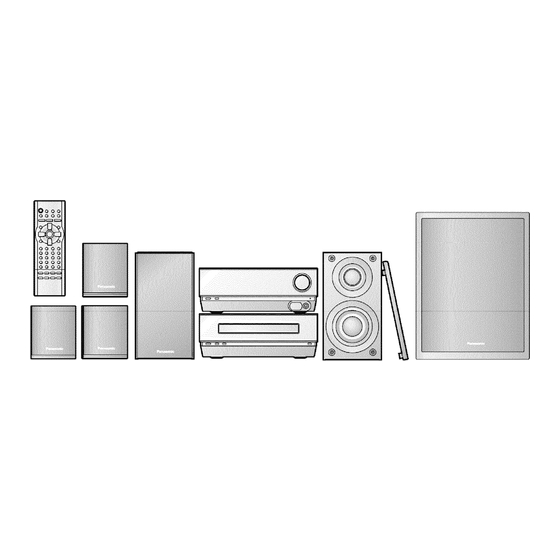
- Page 1 AD0203068C2 AV Control Receiver SA-DT100E / SA-DT100EB / SA-DT100EG Colour (S)..Silver Type SPECIFICATIONS 2002 Matsushita Electric Industrial Co., Ltd. All rights reserved. Unauthorized copying and distribution is a violation of law.
- Page 2 3. Switch ON the power once again. Note: When the protection circuitry functions, the unit will not operate unless the power is first switched OFF and then ON again. 3. Accessories - AC mains lead for SA-DT100E, SA-DT100EG (RJA0019-2X)......1 pc.
- Page 3 - AC mains lead for SA-DT100EB (RJA0053-3X)......1 pc. - AM loop antenna (REK0063)........1 pc. - FM indoor antenna (RSA0007)........1 pc. - Video cable (RJL1P019B15)......1 pc.
- Page 4 - Remote control transmitter (N2QAJB000048)......1 pc. - Remote control batteries (R6/LR6,“AA”, UM-3)....... 2 pcs. Note: These are available on sales route. - Antenna plug adaptor for SA-DT100EB only (SJP9009)......1 pc. - RCAJ adaptor (VFA0151-2)......1 pc.
- Page 5 - Cleaning cloth for main unit (RFE0088-1)......1 pc. - Sheet of speaker-cord stickers (RQCA0950)......1 pc. - Sheet of speaker feet*1 (small, 25 feet)....... 1 pc. - Sheet of speaker feet*1...
- Page 6 (large, 10 feet)......1 pc. Note: The accessories (indicated *1) are packed with SB-DT100. 4. Caution for AC Mains Lead...
- Page 7 5. Location of Controls 6. Self-Diagnostic Function This unit is equipped with a self-diagnostic function which, in the event of a malfunction, automatically displays a code indicating the nature of the malfunction. Use this self-diagnostic function when servicing the unit. 6.1.
- Page 8 6.3. Display contents 6.3.1. U70 DVD - Problem or condition A bus-line communications error has occurred as a result of the flat cable being inserted incorrectly, thus preventing the system from operating. - If U70 is displayed on the AV control receiver, DVD/CD player cannot be operated by remote control.
- Page 9 Procedures - This section describes procedures for checking the operation of the major printed circuit boards and replacing the main components. - For reassembly after operation checks or replacement, reverse the respective procedures. Special reassembly procedures are described only when required. 7.1.
- Page 10 7.2. Checking for the FL P.C.B. - Follow the (Step 1) , (Step 2) of item 7.1. - Check the FL P.C.B. as shown below. 7.3. Checking for the main P.C.B. - Follow the (Step 1) - (Step 7) of item 7.1.
- Page 12 - Check the main P.C.B. as shown below. 7.4. Replacement for the FL P.C.B., headphone P.C.B. and operation P.C.B. - Follow the (Step 1) , (Step 2) of item 7.1. - Follow the (Step 1) , (Step 2) of item 7.2.
- Page 13 8. How to replace IC (TAS5100) with reading terminal block - IC (TAS5100) used in the digital amp P.C.B. has a radiating plate on its backside (the side in contact with the P.C.B.), the radiating terminal block having been soldered to the pattern part of the P.C.B.. / For the replacement of the IC,the following instructions should be observed.
- Page 14 - IC001 - IC006 shown in the drawing below are ICs each equipped with a radiating terminal block. [Disassembly] 1. Use a blower and heat the IC (about 20 seconds). 2. In about the 20 seconds, the legs of the IC begin fusing. Then remove the IC by use of a pair of tweezers.
- Page 15 1. Put solder-paste thinly and evenly over the radiating plate on the bottom of a new IC for replacement. 2. Clean out the former solder that has been sticking to the pattern part on the base plate. 3. Place the IC on the pattern part of the base plate. / (Make the IC legs and pattern part meet completely.) 4.
- Page 16 9. To Supply Power Source This unit is designed to operate on power supplied from system connected. / When a component requires service, use the system connections to supply power source. / For system connections, refer to Fig.9-1. Fig. 9-1. 10.
- Page 17 Furthermore, special parts which have purposes of fire-retardant (resistors), high-quality sound (capacitors), low-noise (resistors), etc. are used. When replacing any of components, be sure to use only manufacturer´s specified parts shown in the parts list. - The supply part number is described alone in the replacement parts list. - Voltage and signal line : Positive voltage line : Negative voltage line...
- Page 18 12. Printed Circuit Board Diagram 13. Type Illustration of ICs, Transistors and Diodes 14. Wiring Connection Diagram 15. Block Diagram 16. Terminal Function of ICs 16.1. IC941(C2CBHG000095): / System Control Function Terminal Name 1 FL SCK Clock signal output for IC901 FL CS Chip select signal output for IC901...
- Page 19 Function Terminal Name Not used, open 22 PMD / Not used 23 PMD / Not used DOUT 24 DVD& / DVD communication data signal AMP / output D OUT 25 DVD D DVD communication data signal input 26 DVD& / DVD communication clock AMP / signal input...
- Page 20 Function Terminal Name CR timer signal input TIMER Not used, connected to GND Not used, connected to GND Not used, connected to GND Not used, connected to GND Not used, connected to GND LED drive signal output STBY LED drive signal output TIMER 57 LED / LED drive signal output...
- Page 21 <IB>: Swedish, Netherlands, Danish <IC>: English <ID>: Spanish, Polish, Czech - The parenthesized indications in the Remarks columns specify the areas. (E): SA-DT100E (EB): SA-DT100EB (EG): SA-DT100EG - The marking in Ref No. indicate as follow. *2: FL circuit - The marking [RTL] indicates the retention time is limited for this item.
- Page 22 Ref. No. Part No. Part Name & Description Remarks XTB3+8JFZ SCREW REM0106 FAN UNIT REZ1446 RGK1508-K BOTTOM COVER RGN2259-K NAME PLATE RGN2258-K NAME PLATE (EB) RGN2257-K NAME PLATE (EG) RGR0329B-A1A REAR PANEL RHD30078 SCREW RKA0137-K RUBBER RMA1538 FAN ANGLE RMC0471 ANGLE RMN0696 HOLDER 1...
- Page 23 Ref. No. Part No. Part Name & Description Remarks RQT6385-D OPERATING / INSTRUCTIONS <IA>(EG) RQT6386-H OPERATING / INSTRUCTIONS <IB>(EG) RQT6387-B OPERATING / INSTRUCTIONS <IC>(E,EB) RQT6388-R OPERATING / INSTRUCTIONS <ID>(E) SJP9009 ANTENNA PLUG / ADAPTOR K1YZ02000013 (EB) C001,02 ECUVNH103KBV 50V 0.01U F1H1H103A748 C003,04 F1H1H333A783...
- Page 25 Ref. No. Part No. Part Name & Description Remarks C151,52 ECST1AY475R 10V 4.7U C153,54 ECJ1VB1C104K 16V 0.1U C155,56 ECST1AY475R 10V 4.7U C157,58 ECJ1VB1C104K 16V 0.1U C159-62 ECST1AY475R 10V 4.7U C175 ECJ1VB1C104K 16V 0.1U C177 ECJ1VB1H102K 50V 1000P C180 ECJ1VB1H681K 50V 680P C181 ECUV1H470JCV 50V 47P...
- Page 27 Ref. No. Part No. Part Name & Description Remarks C361-63 ECA1CAK100XB 16V 10U C365 ECST1CY225R 16V 2.2U C367 ECA1CAK100XB 16V 10U C368 RCE1HKA4R7BG 50V 4.7U F2A1H4R70009 C370 RCE1HKA4R7BG 50V 4.7U F2A1H4R70009 C371 ECST1AY106R 10V 10U C378 RCE1HKA4R7BG 50V 4.7U F2A1H4R70009 C379 ECJ1VB1H822K 50V 8.2K...
- Page 28 Ref. No. Part No. Part Name & Description Remarks C622 ECJ1VB1H222K 50V 2200P C623 ECUVNE223KBV 25V 0.022U F1H1E223A050 C624 ECJ1VB1C104K 16V 0.1U C625 ECUVNH103KBV 50V 0.01U F1H1H103A748 C626 ECA1AAK221XH 10V 220U C628 ECA0JAK101XB 6.3V 100U C629 RCE0JKA470BG 6.3V 47U F2A0J470A014 C630 ECUVNJ105KBV 6.3V 1U...
- Page 29 Ref. No. Part No. Part Name & Description Remarks C757 RCE1VKA100BG 35V 10U F2A1V1000011 C761,62 F1J1H104A679 50V 0.1U C763 ECUVNH103KBV 50V 0.01U F1H1H103A748 C901-04 ECA1EAK220XB 25V 22U C905 ECST1AY475R 10V 4.7U C906 ECUVNH103KBV 50V 0.01U F1H1H103A748 C907 ECJ1VB1C104K 16V 0.1U C908 ECUVNH103KBV 50V 0.01U...
- Page 31 Ref. No. Part No. Part Name & Description Remarks D501 MAZ80510LL DIODE D541 MA8051M DIODE MAZ80510M D701-05 RL1N4003N02 DIODE B0AAMM000009 D708 MAZ80680LL DIODE D709 MA2J11100L DIODE D710 1SS380TE-17 DIODE D711-15 RL1N4003N02 DIODE B0AAMM000009 D722 MA8043M DIODE MAZ80430M D725 MA143TX DIODE MA3J14300L D727 MAZ83000HL...
- Page 32 Ref. No. Part No. Part Name & Description Remarks IC303,04 NJM4558MTE1 C0ABBB000109 IC305 M5218AP C0AABB000055 IC501 M62444FPE1 C1BB00000386 IC541 C1BB00000527 IC601 C2HBZC000013 IC722 C0CBADE00034 IC723 C0CBADE00031 IC725 C0CBAHE00002 IC726 C0CBADE00034 IC727 C0CBABC00119 IC728 C0CBAEE00004 IC729 C0CBAEE00003 IC901 C0HBB0000030 IC941 C2CBHG000095 JK101 K1FA612B0002 JK,SP TERMINAL...
- Page 33 Ref. No. Part No. Part Name & Description Remarks Q701 B1ABGC000001 TRANSISTOR Q702 UNR521100L TRANSISTOR Q704 2SC3940ARSTA TRANSISTOR 2SC3940AHA Q721 2SD1819A0L TRANSISTOR Q722 B1BCAJ000003 TRANSISTOR Q724 B1BCAJ000003 TRANSISTOR Q726 2SB621RSTA TRANSISTOR 2SB06210HA Q727 2SD1819A0L TRANSISTOR Q729 2SA20570P TRANSISTOR Q731 XN0450100L TRANSISTOR Q733 2SA20570P...
- Page 35 Ref. No. Part No. Part Name & Description Remarks R157-59 ERJ3GEYJ242V 1/16W 2.4K R161-66 ERJ3GEYJ102V 1/16W 1K R167 ERJ3GEYJ332V 1/16W 3.3K D0GB332JA002 R175-78 ERJ3GEYJ392V 1/16W 3.9K R179,80 ERJ3GEYJ102V 1/16W 1K R181-84 ERJ3GEYJ682V 1/16W 6.8K D0GB682JA002 R188 ERJ3GEY0R00V CHIP JUMPER R190,91 ERJ3GEY0R00V CHIP JUMPER R201,02...
- Page 37 Ref. No. Part No. Part Name & Description Remarks R370 ERJ3GEYJ332V 1/16W 3.3K D0GB332JA002 R371 ERJ3GEYJ104Z 1/16W 100K R372 ERJ3GEYJ152V 1/16W 1.5K R373 ERJ3GEYJ183V 1/16W 18K D0GB183JA002 R374 ERJ3GEYJ104Z 1/16W 100K R375 ERJ3GEYJ272V 1/16W 2.7K R376 ERJ3GEYJ332V 1/16W 3.3K D0GB332JA002 R377 ERJ3GEYJ223V 1/16W 22K...
- Page 39 Ref. No. Part No. Part Name & Description Remarks R510 ERJ3GEY0R00V CHIP JUMPER R511 ERJ3GEYJ332V 1/16W 3.3K D0GB332JA002 R512 ERJ3GEYJ123V 1/16W 12K R515 ERJ3GEYJ332V 1/16W 3.3K D0GB332JA002 R516 ERJ3GEYJ123V 1/16W 12K R519 ERJ3GEYJ391V 1/16W 390 R520,21 ERJ3GEYJ472V 1/16W 4.7K R523 ERJ3GEYJ472V 1/16W 4.7K R525,26...
- Page 40 Ref. No. Part No. Part Name & Description Remarks R741 ERJ3GEYJ471V 1/16W 470 R745 ERJ3GEY0R00V CHIP JUMPER R747 ERJ3GEYJ103Z 1/16W 10K R829,30 ERJ3GEYJ104Z 1/16W 100K R839 ERJ3GEYJ103Z 1/16W 10K R851 ERJ3GEYJ103Z 1/16W 10K R852,53 ERJ3GEYJ472V 1/16W 4.7K R854 ERJ3GEYJ103Z 1/16W 10K R855 ERJ3GEYJ473V 1/16W 47K...
- Page 42 Ref. No. Part No. Part Name & Description Remarks R966 ERJ3GEYJ101V 1/16W 100 R967 ERJ3GEYJ103Z 1/16W 10K R968-70 ERJ3GEYJ101V 1/16W 100 R971 ERJ3GEYJ103Z 1/16W 10K R972 ERJ3GEYJ222V 1/16W 2.2K R973 ERJ3GEYJ824V 1/16W 820K D0GB824JA002 R974-76 ERJ3GEYJ103Z 1/16W 10K R977 ERJ3GEYJ101V 1/16W 100 R978,79 ERJ3GEYJ103Z...
- Page 43 Ref. No. Part No. Part Name & Description Remarks VR901 EVEKC2F3024B VR,VOLUME X131 H0H245500013 OSCILLATOR X132 H0H254500002 OSCILLATOR X541 RSXC4M33S02T OSCILLATOR H0H433400001 X601 RSXZ36M8M01T OSCILLATOR X942 H2B100500004 OSCILLATOR Z001 J0JBC0000015 COMPONENT / COMBINATIONS Z002,03 VLP0155-T COIL J0JCC0000119 Z004-08 J0JBC0000015 COMPONENT / COMBINATIONS Z701 ERZV10V511CS COMPONENT / COMBINATIONS...
- Page 44 19. Packaging...
- Page 45 20. Schematic Diagram for printing with letter size F020300000YM/KH...
- Page 46 C0CBAEE00004 C0CBABC00119 NJU7313AMT2 30PIN M62456FPE1 24PIN C0HBB0000030 64PIN C1BB00000527 16PIN C0ZBZ0000647 32PIN NJM4558MTE1 8PIN C0FBAJ000009 14PIN M62444F PE1 42PIN C0FBAK000008 20PIN M5218AP 8PIN TC7WH74FUTL 8PIN No.1 No.1 C0JBAB000423 C0DAZZC00003 C2CBHG000095 80PIN C0CBAEE00003 AHCTG08DBV C2HBZC000013 80PIN C0CBAHE00002 C0JBAD000153 C0ZBZ0000650 48PIN C0CBADE00034 C0JBAZ001870 C0CBADE00031 No.1...
- Page 47 SCHEMATIC DIAGRAM-1 FL CIRCUIT FL901(A2BC00000048) FL DISPLAY 5 6 7 8 9 10 11 12 13 14 15 16 17 18 19 20 21 22 23 24 25 26 27 28 29 30 31 32 33 34 35 36 37 38 39 40 41 42 43 44 45 46 47 48 49 50 51 52 53 54 55 56...
- Page 48 :NEGATIVE VOLTAGE LINE MAIN CIRCUIT :POSITIVE VOLTAGE LINE :AUDIO SIGNAL LINE :FM SIGNAL LINE :AM SIGNAL LINE R546 R541 L542 L541 C549 0.3V 5.2V 5.2V 2.5V IC541 C1BB00000527 RDS SIGNAL DEMODULATOR 2.6V 2.6V 5.2V 2.6V 2.6V 2.7V C550 RJ49 C545 C544 560P 6.3V47...
- Page 49 SCHEMATIC DIAGRAM-2 MAIN CIRCUIT To TUNER CIR To SL-DT100 (CN1) on SCHEMATI 4 5 6 7 8 9 10 11 12 13 14 15 16 17 18 19 CN301 RJ42 R416 R415 R355 R404 C646 R621 50V1 C647 50V1 R622 C602 R601 50V1...
- Page 50 :NEGATIVE VOLTAGE LINE :POSITIVE VOLTAGE LINE :AUDIO SIGNAL LINE :FM SIGNAL LINE :AM SIGNAL LINE To TUNER CIRUIT(CP301) on SCHEMATIC DIAGRAM-10/9-A 8 19 CP301 R615 100K L602 C611 0.022 C623 0.022 RJ48 C646 R621 50V1 2.4V LIN4 ELR I/ O 2.4V LIN3 SYNC...
- Page 51 SCHEMATIC DIAGRAM-3 MAIN CIRCUIT :POSITIVE VOLTAGE LINE :NEGATIVE VOLTAGE LINE :AUDIO SIGNAL LINE R992 A B C J K L M R713 100K R999 100K R998 R941 R939 R943 D949 MAZ80510LL Q941 UN5214TX C954 RESET 220P C952 5.1V R945 50V3.3 C956 220P C941...
- Page 52 C347 IC303 R362 NJM4558MTE1 R364 R363 RJ38 C361 2.7K 3.3K 16V10 BUFFER AMP Q301 B1GFGCAA0001 -6.1V MUTING -6.2V -6.2V 5.9V R356 R358 R357 C359 2.7K 3.3K 16V10 C345 C353 IC304 NJM4558MTE1 R375 R373 R372 RJ36 C363 2.7K 1.5K 16V10 BUFFER AMP Q302 B1GFGCAA0001 -6.1V...
- Page 53 SCHEMATIC DIAGRAM-4 MAIN CIRCUIT :POSITIVE VOLTAGE LINE :NEGATIVE VOLTAGE LINE :AUDIO SIGNAL LINE -6.3V -6.3V D302,303 C321 R335 C323 R339 MA111TX 16V10 0.068 8.2K D302 D301 R341 R346 MA111TX 8.2K Q305 D303 B1GFGCAA0001 R390 MUTING R383 C327 C329 C335 100P 470P 10V33 -6.2V...
- Page 54 IC722 IC723 IC726 IC727 C0CBADE00034 C0CBADE00031 C0CBADE00034 C0CBABC00119 REGULATOR REGULATOR REGULATOR REGULATOR IC728 C0CBAEE00004 VOUT VOUT VOUT VOUT OU T REGULATOR 8.5V 8.5V 8.5V 3.3V 8.5V 8.5V 6.1V C748 C751 C726 C754 C762 C755 C749 C744 C740 0.33 10V4.7 L721 3.3V L722 Q722...
- Page 55 SCHEMATIC DIAGRAM-5 MAIN CIRCUIT :POSITIVE VOLTAGE LINE :NEGATIVE VOLTAGE LINE :AUDIO SIGNAL LINE CN720 R471 R472 DIGITAL AMP CIRCUIT(CN102) on SCHEMATIC DIAGRAM-6/2-A~C FRQ SHIFT MUTE FRNT MUTE REAR MUTE SUB +B(5V) +B(3.3V) 3.3V SHTDWN R716 RJ56 GATE BIAS FAN DET W705 DIGITAL AMP CIRCUIT(CN101) on SCHEMATIC DIAGRAM-6/2-D...
- Page 56 GITAL AMP CIRCUIT(CN102) MATIC DIAGRAM-6/2-A~C GITAL AMP CIRCUIT(CN101) MATIC DIAGRAM-6/2-D OWER TORANSFORMER CIRCUIT T701 CN710 AC20.6V CN709 FP701 CN708 CN713 AC12.3V CN707 CN715 CN706 AC30V R714 CN705 CN712 CN704 AC4.2V CN703 CN714 R712 IN CIRCUIT Q701 B1ABGC000001 RL702 RELAY DRIVE R702 3.9K 0.7V...
- Page 57 SCHEMATIC DIAGRAM-6 DIGITAL AMP CIRCUIT :POSITIVE VOLTAGE LINE :AUDIO SIGNAL LINE R142 R190 C1016 2.1V 4.6V 4.6V 1.2V C1015 IC022 C1014 C0FBAJ000009 16bit A / D CONVERTER 3.2V R163 C141 16V1 C1013 IC02 2.1V 2.1V 4.6V 1.5V 1.6V 1.6V LOGIC (D-TY R164 C142...
- Page 58 3.2V 3.2V 3.2V Q002 Q001 XN0431100L UN5111TX SWITCHING SWITCHING 3.2V 3.2V 0.6V 0.6V 3.2V IC019 IC017 IC018 C0JBAB000423 C0JBAD000153 C0JBAB000423 Z002 INVERTER NOR GATE INVERTER 3.2V 3.2V 3.2V 1.4V 0.6V 1.3V 3.2V 1.3V IC020 TC7WH74FUTL LOGIC CONT. (D-TYPE FLIP FLOP) 1.4V 1.6V 3.2V...
- Page 59 SCHEMATIC DIAGRAM-7 DIGITAL AMP CIRCUIT :POSITIVE VOLTAGE LINE :AUDIO SIGNAL LINE 3.2V IC001 C0ZBZ0000647 TRUE DIGITAL AMP D1021 R1021 MAZ80510LL 1.6V 26.7V PWM AP C007 1.6V 14.9V PWM AM LDROUTA C009 0.033 BOOTSTRAPA ERR1 3.1V 26.7V ERR0 R003 C011 3.1V 26.7V SHUTDOWN R101...
- Page 60 C128 1.6V 3.2V MCLK IN 1.6V PWM P L 1.8V 1.6V PLL FLT OUT PWM M L PLL FLT RET IC012 AVss2 C0ZBZ0000650 3.2V 2.9V DIGITAL AUDIO / RESET DVss2 PWM PROCESSOR 3.2V 1.6V / PDN PWM P R 3.2V 1.6V VALID R PWM N R...
- Page 61 SCHEMATIC DIAGRAM-8 DIGITAL AMP CIRCUIT :POSITIVE VOLTAGE LINE :AUDIO SIGNAL LINE 3.2V IC003 C0ZBZ0000647 TRUE DIGITAL AMP D1025 R1025 MAZ80510LL 1.6V 26.7V PWM AP C037 1.6V 14.9V PWM AM LDROUTA C039 0.033 BOOTSTRAPA ERR1 3.1V 26.7V ERR0 R013 C041 3.1V 26.7V SHUTDOWN R111...
- Page 62 C129 1.6V 3.2V MCLK IN 1.6V PWM P L 1.8V 1.6V PLL FLT OUT PWM M L PLL FLT RET IC013 AVss2 C0ZBZ0000650 3.2V 2.9V DIGITAL AUDIO / RESET DVss2 PWM PROCESSOR 3.2V 1.6V / PDN PWM P R 3.2V 1.6V VALID R PWM N R...
- Page 63 SCHEMATIC DIAGRAM-9 DIGITAL AMP CIRCUIT :POSITIVE VOLTAGE LINE :AUDIO SIGNAL LINE IC005 C0ZBZ0000647 TRUE DIGITAL AMP D1029 R1029 MAZ80510LL 1.6V 26.7V PWM AP C067 1.6V 14.9V PWM AM LDROUTA C069 0.033 BOOTSTRAPA ERR1 3.1V 26.7V ERR0 R023 C071 3.1V 26.7V SHUTDOWN R121 3.1V...
- Page 64 JK101 SPEAKERS FRONT HF/ LF(6 ) SURROUND(6 ) CENTER(6 ) SUB WOOFER(6 ) SP FRAME SA-DT100(E,EB,EG) DIGITAL AMP CIRCUIT DIAGRAM...
- Page 65 SCHEMATIC DIAGRAM-10 TUNER MODULE CIRCUIT(Z1001 ENG07701Q) 2SC2059 FM MIXER ~ 680 ~ 220 FM ANT (75 ) 2SK360 RF AMP 2SC2413 or 2SC3053 BUFFER AMP AM ANT LOOP 270P ~ 560P 1000P 5.6K 0.01 100P LC72131M PLL FREQUENCY SYNTHESIZER 7.2MHz 3.3K...
- Page 66 :POSITIVE VOLTAGE LINE :FM SIGNAL LINE :AM SIGNAL LINE :AM OSC SIGNAL LINE :FM OSC SIGNAL LINE ~ 680 100K ~ 470K ~ 1K 1000P 2SC2413 or DTA114 or 2SC3053 RT1P141C FM IF AMP POWER SUPPLY (FM:ON) ~ 100 220 ~ 1000P 10K ~ 220 ~...
- Page 67 SCHEMATIC DIAGRAM-10 TUNER MODULE CIRCUIT(Z1001 ENG07701Q) :POSITIVE VOLTAGE LINE :FM SIGNAL LINE :AM SIGNAL LINE :AM OSC SIGNAL LINE :FM OSC SIGNAL LINE 2SC2059 FM MIXER ~ 680 ~ 220 100K ~ 470K ~ 1K FM ANT (75 ) 1000P 2SK360 RF AMP 2SC2413 or...
- Page 68 SCHEMATIC DIAGRAM-9 DIGITAL AMP CIRCUIT :POSITIVE VOLTAGE LINE :AUDIO SIGNAL LINE IC005 C0ZBZ0000647 TRUE DIGITAL AMP D1029 R1029 MAZ80510LL 1.6V 26.7V PWM AP C067 1.6V 14.9V PWM AM LDROUTA C069 0.033 BOOTSTRAPA ERR1 3.1V 26.7V ERR0 R023 C071 3.1V 26.7V SHUTDOWN R121 3.1V...
- Page 69 SCHEMATIC DIAGRAM-8 DIGITAL AMP CIRCUIT :POSITIVE VOLTAGE LINE :AUDIO SIGNAL LINE 3.2V IC003 C0ZBZ0000647 TRUE DIGITAL AMP D1025 R1025 MAZ80510LL 1.6V 26.7V PWM AP C037 1.6V 14.9V PWM AM LDROUTA C039 0.033 BOOTSTRAPA ERR1 3.1V 26.7V C129 ERR0 R013 C041 3.1V 26.7V SHUTDOWN...
- Page 70 SCHEMATIC DIAGRAM-7 DIGITAL AMP CIRCUIT :POSITIVE VOLTAGE LINE :AUDIO SIGNAL LINE 3.2V IC001 C0ZBZ0000647 TRUE DIGITAL AMP D1021 R1021 MAZ80510LL 1.6V 26.7V PWM AP C007 1.6V 14.9V PWM AM LDROUTA C009 0.033 BOOTSTRAPA ERR1 3.1V 26.7V ERR0 R003 C011 3.1V 26.7V SHUTDOWN R101...
- Page 71 SCHEMATIC DIAGRAM-6 DIGITAL AMP CIRCUIT :POSITIVE VOLTAGE LINE :AUDIO SIGNAL LINE R142 3.2V 3.2V 3.2V R190 Q002 Q001 XN0431100L UN5111TX SWITCHING SWITCHING 3.2V C1016 3.2V 0.6V 2.1V 4.6V 4.6V 1.2V 0.6V 3.2V C1015 IC019 IC017 IC018 C0JBAB000423 C0JBAD000153 C0JBAB000423 Z002 IC022 INVERTER NOR GATE...
- Page 72 SCHEMATIC DIAGRAM-5 MAIN CIRCUIT :POSITIVE VOLTAGE LINE :NEGATIVE VOLTAGE LINE :AUDIO SIGNAL LINE CN720 R471 R472 DIGITAL AMP CIRCUIT(CN102) on SCHEMATIC DIAGRAM-6/2-A~C FRQ SHIFT MUTE FRNT MUTE REAR MUTE SUB +B(5V) 3.3V +B(3.3V) SHTDWN R716 RJ56 GATE BIAS FAN DET W705 DIGITAL AMP CIRCUIT(CN101) on SCHEMATIC DIAGRAM-6/2-D...
- Page 73 SCHEMATIC DIAGRAM-4 MAIN CIRCUIT :POSITIVE VOLTAGE LINE :NEGATIVE VOLTAGE LINE :AUDIO SIGNAL LINE -6.3V -6.3V IC722 IC723 IC726 IC727 C0CBADE00034 C0CBADE00031 C0CBADE00034 C0CBABC00119 REGULATOR REGULATOR REGULATOR REGULATOR D302,303 C321 R335 C323 R339 MA111TX IC728 16V10 0.068 8.2K C0CBAEE00004 D302 VOUT VOUT VOUT VOUT...
- Page 74 SCHEMATIC DIAGRAM-3 MAIN CIRCUIT :POSITIVE VOLTAGE LINE :NEGATIVE VOLTAGE LINE :AUDIO SIGNAL LINE C347 R992 A B C J K L IC303 100K R713 R362 NJM4558MTE1 R364 R363 RJ38 C361 2.7K 3.3K 16V10 R999 100K R998 BUFFER AMP Q301 R941 B1GFGCAA0001 R939 R943...
- Page 75 SCHEMATIC DIAGRAM-2 :NEGATIVE VOLTAGE LINE MAIN CIRCUIT :POSITIVE VOLTAGE LINE :AUDIO SIGNAL LINE :FM SIGNAL LINE :AM SIGNAL LINE To TUNER CIRUIT(CP301) To SL-DT100 (CN1) on SCHEMATIC DIAGRAM-10/9-A 4 5 6 7 8 9 10 11 12 13 14 15 16 17 18 19 CN301 CP301 R615...
- Page 76 SCHEMATIC DIAGRAM-1 :NEGATIVE VOLTAGE LINE FL CIRCUIT MAIN CIRCUIT :POSITIVE VOLTAGE LINE :AUDIO SIGNAL LINE :FM SIGNAL LINE :AM SIGNAL LINE FL901(A2BC00000048) FL DISPLAY R546 R541 5 6 7 8 9 10 11 12 13 14 15 16 17 18 19 20 21 22 23 24 25 26 27 28 29 30 31 32 33 34 35 36 37 38 39 40 41 42 43 44 45 46 47 48 49 50 51 52 53 54 55 56...
- Page 77 HEADPHONE P.C.B. JK901 AC IN P.C.B. (SIDE:A) AC IN P.C.B. (SIDE:B) (RL702) RL702 (W1) Z901 Q701 C916 T702 (POWER TRANSFORMER) (T702) (POWER TRANSFORMER) R715 R745 CN904 C702 Q702 (REP3348A-S) R704 R705 R706 (CN702) CN702 (D701) (D702) (Z701) D701 D702 Z701 (W2/W3/W4) W2/W3/W4 (C704)
- Page 78 DIGITAL AMP P.C.B. (SIDE:A) DIGITAL AMP P.C.B. (SIDE:B) CN102 (CN102) 8 10 12 14 16 18 20 22 24 R178 R177R176R175 R058 (CN101) CN101 L103 C019 R107 R1020 C140 C103 C188 R162 D1020 R105 C139 C187 C162 R161 R103 C005 C1040 (Q051) IC051...
- Page 79 MAIN P.C.B. (SIDE:B) CP702 D729 D752 D753 D730 Q724 Q729 Q733 D733 D735 E C B E C B Q722 C730 R738 RJ50 D728 D734 L604 C611 C630 C623C614 CN301 C635 IC601 Q304 To SL-DT100 C746 C609 C616 C624 Q303 WA721 C621 D738...
- Page 80 Note: This printed circuit board diagram may be modified at any time with the development of new technology. FL P.C.B. MAIN P.C.B. (SIDE:A) C904 Q904 D903 Q456 Q453 CN903 D451 D751 (CP702) C903 VR901 RJ73 Q454 R465 Q455 (Q724) Q721 C909 R922 IC723...
- Page 81 TUNER MODULE (Z1001 ENG07701Q) FM ANT AM ANT +B(FM) RF AMP FM MIXER TU B COIL COIL +B(FM) FM IF LA1833MN +B(FM) C1BB00000527 BUFFER FM / AM I F AMP, LOCAL OSC TU B IC541 DET / AM OSC, RDS SIGNAL DEMODULATOR MIX / FM MPX +B(FM) 3,11...
- Page 82 NJU7313AMT2 IC201 SIGNAL SELECTOR (29) CN301 (28) TV IN SL SYNC SYNC CD REQ (27) CT.GND (26) (25) NJM4558MTE1 IC202 DC10V DVD 10V (24) (22) BUFFER FL901 DC GND FL DISPLAY (23) Q731,942 SCLK (20) DATA SWITCHING Q901 AMP REQ POWER (EXT) (21)
- Page 83 DSP D5V M62456FPE1 HEADPHONE IC302 R ch PRE AMP TU B Q305,314 CR NETWORK MUTING LIN4 (69) (RIN4) 19 22 DSP D5V M5218AP LIN3 (70) (RIN3) MICU I/F AUDIO SERIAL INTERFACE IC305 DSP D5V VDA12 LIN2 BUFFER (71) (RIN2) LIN1 DELAY RAM (72) (RIN1)
- Page 84 C0FBAK000008 C0JBAD000153 C0JBAB000423 C0JBAB000423 IC024 IC017 IC019 IC018 24bit A/D CONVERTER NOR GATE INVER- INVER- DOUT SINGLE-END 5th ORDER 1(2) VINL(R) /DIFFERENTIAL DELTA-SIGMA R ch x164(x1/128) CONVERTER MODULATOR C0ZBZ0000650 DECIMATION SERIAL IC011 FILTER WITH LRCK INTERFACE X131 VREF1 X132 DIGITAL AUDIO PWM PROCESSOR DC CUT /MODE/ FILTER...
- Page 85 28,29 C0ZBZ0000647 28,29 IC001(IC002) TRUE DIGITAL AMP BOOT- C0ZBZ0000647 BOOT- STRAPA IC005 STRAPA TRUE DIGITAL AMP PWM AP OUTPUTA 26,27 PWM AP OUTPUTA 26,27 DIFF BOOT STRAP DIFF RCVR FRONT HF/LF BOOT STRAP PWM AM CENTER GATE DRIVE RCVR PWM AM SPEAKERS GATE DRIVE SPEAKER...
- Page 86 Q051 D714,715 REGULATOR T701 C0DAZZC00003 D738 STABILIZER IC051 C0CBABC00119 IC727 FAN DET REGULATOR C0CBAHE00002 IC725 D733 C0CBAEE00004 IC728 TU B REGULATOR REGULATOR Q727,729,733 D735 C0CBADE00034 REGULATOR DVD 10V IC722 /STABILIZER AC IN L701 D729 L722 D711,712 DSP D5V REGULATOR D730 C0CBAEE00003 RLY702 D752...
- Page 88 HEADPHONE P.C.B. CN904 7 ..1 7 ..1 7 ..1 CN903 FL P.C.B. CN902 2 . . . 10 1 . . . 9 CN901 11 ..1 12 .
Need help?
Do you have a question about the SA-DT100E and is the answer not in the manual?
Questions and answers