Advertisement
Quick Links
SPECIFICATIONS
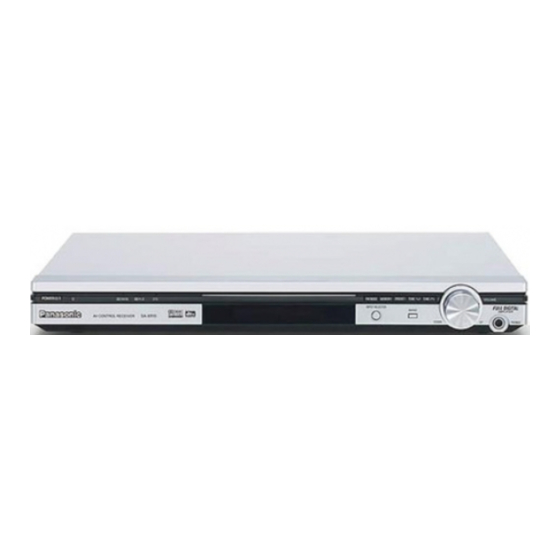
SA-XR15E / SA-XR15EB / SA-XR15EG
AMPLIFIER SECTION
Power output (at AC 230-240V)
DIN 1 kHz (T.H.D. 1 %)
20 Hz-20 kHz continuous power
output both channels driven
Total harmonic distortion
rated power at 20 Hz-20 kHz
Power output each channel driven
DIN 1 kHz (T.H.D. 1 %)
Front (L/R)
Center
Surround (L/R)
10 % total harmonic distortion at 1
kHz
Front (L/R)
Center
Surround (L/R)
Load impedance
Front (L/R)
Center
Surround (L/R)
Frequency response
DVD, TV, VCR, AUX
Input sensitivity and impedance
ORDER NO. MD0305192C2
(S).......................Silver Type
(K).......................Black Type
Specification
2 x 40 W (6
2 x 35 W (6
10 Hz-44 kHz, ±3 dB
1
AV Control Receiver
)
)
0.9 % (6
)
40 W (6
)
40 W (6
)
40 W (6
)
50 W (6
)
50 W (6
)
50 W (6
)
6-16
6-16
6-16
Colour
Advertisement

Subscribe to Our Youtube Channel
Related Manuals for Panasonic SA-XR15E


Summary of Contents for Panasonic SA-XR15E
- Page 1 ORDER NO. MD0305192C2 AV Control Receiver SA-XR15E / SA-XR15EB / SA-XR15EG Colour (S).......Silver Type (K).......Black Type SPECIFICATIONS Specification AMPLIFIER SECTION Power output (at AC 230-240V) DIN 1 kHz (T.H.D. 1 %) 2 x 40 W (6 20 Hz-20 kHz continuous power...
- Page 2 200 mV / 22 k DVD, TV, VCR, AUX S/N at rated power (6 DVD, TV (Digital Input) 90 dB (IHF, A:96 dB) Tone controls BASS 50 Hz, +10 to -10 dB TREBLE 20 kHz, +10 to -10 dB Output voltage 200 mV ±1 dB Channel balance (250 Hz-6.3 kHz)
- Page 3 1. Specifications are subject to change without notice. Mass and dimensions are approximate. 2. Total harmonic distortion is measured by the digital spectrum / analyzer. 2003 PANASONIC AVC Networks Singapore Pte. Ltd. All rights reserved. Unauthorized copying and distribution is a violation of law. 1. SAFETY PRECAUTIONS 1.1.
- Page 4 2. After servicing, see to it that all the protective devices such as insulation barriers, insulation papers shields are properly installed. 3. After servicing, make the following leakage current checks to prevent the customer from being exposed to shock hazards. 1.1.1.
- Page 5 6. The potential at any point should not exceed 0.75 volts RMS. A leakage current tester (Simpson Model 229 or equivalent) may be used to make the hot checks, leakage current must not exceed 1/2 milliamp. In case a measurement is outside of the limits specified, there is a possibility of a shock hazard, and the equipment should be repaired and rechecked before it is returned to the customer.
- Page 6 2. Determine the cause of the problem and correct it. 3. Press the STANDBY /ON button once again, supply the power. Note: When the protection circuitry functions, the unit will not operate unless the STANDBY button is first switched STANDBY and then ON again. 5.
- Page 7 Antenna plug adapter / ..1 pcs (EG) Remote control / ..1 pc 6. Caution for AC Mains Lead...
- Page 8 7. Operation Procedures 8. Disassembly and Main Component Replacement Procedures and Operational Check “ATTENTION SERVICER” Some chassis components may have sharp edges. Be careful when disassembling and servicing.
- Page 9 - This section describes procedures for checking the operation of the major printed circuit boards and replacing the main components. - For reassembly after operation checks or replacement, reverse the respective procedures. Special reassembly procedures are described only when required. Contents - Checking for the Main PCB and DSP PCB - Checking for the Input output PCB...
- Page 10 Step 5 : Remove the screws. Step 6 : Release the claws of P.C.B. support and remove the DSP P.C.B. - Check the DSP P.C.B. (Side B) as shown below. Step 7 : Remove the screw and Decorder Angle for checking Digital AMP P.C.B. 8.2.
- Page 11 Step 1 : Remove the connector (CP500). Step 2 : Remove all the screws. Step 3 : Remove the rear panel. Step 4 : Remove all the screws. Step 5 : Turn up the Input P.C.B. - Check the Input P.C.B. as shown below. 8.3.
- Page 12 * Repeat step 1 to step 7 for 8.1. * Repeat step 1 to step 3 for 8.2. Step 1 : Remove the screw and Heat Barrier. Step 2 - 4 : Remove all the screws. Step 5 : Remove the flat-cable from the connector (CN951B).
- Page 13 Step 6 : Remove all the screws. Step 7 : Remove all the connectors (CN951B, CN901 and CN902). Step 8 : Release the 2 claws and remove the front panel ass’y. Step 9 : Remove the volume knob. Step 10 : Remove the nut. Step 11 : Remove all the screws.
- Page 14 Step 13 : Release the claws of the P.C.B. support. Step 14 : Release the connector (CN952) and remove the FL P.C.B. Step 15 : Remove all the screws and Light Guide Unit. Step 16 : Remove all the screws. Step 17 : Remove the Volume P.C.B.
- Page 15 Step 18 : Turn the Power Supply P.C.B. as arrow shown above. - Check the Power Supply P.C.B. as shown below. Step 19 : Connect back the connectors (CN952, CN902, CN901 and CN951B). 9. Self Diagnosis Display Function This unit is equipped with the self diagnosis display function, which alarms faulty operation with error code.
- Page 16 9.2. Display Details Refer to the following table. LCD display Symptom Cause and Remedy OVERLOAD Speaker short, amplifier failure Speaker short and failure in power amplifier, pre-amplifier Humidity protection activated circuits. Check for faulty parts and replace with new parts if necessary.
- Page 17 indicates the ROM checksum used for ROM collection, and if the unit is not loaded with ROM, "NO" appears. When the TUNING UP button is pressed, the sub micro computer program filing number (ex. S90_***" for MA678_90) appears. The ** * digit indicates the ROM checksum used for ROM collection, and if the unit is not loaded with ROM, "NO"...
- Page 18 unit measured by DC electronic voltmeter (high impedance) and oscilloscope on the basis of chassis. Accordingly, there may arise some error in voltage values and waveforms depending upon the internal impedance of the tester or the measuring unit. - Importance safety notice : Components identified by mark have special characteristics important for safety.
- Page 19 Terminal Function Name LED_CK O LED Driver Control : Clock LED_DT LED Driver Control : Data LED_ST I/O LED Driver Control : Strobe E_DT O EEPROM Control : Data E_CK O EEPROM Control : Clock E_CS O EEPROM Control : Chip Select REQS I/O Communication to Sub up :...
- Page 20 Terminal Function Name M_RESET O RESET signal for sub up FAN_CTRL O Cooling Fan Control Output HP_SW Headphone Detection MT_2ND O MUTE for 2nd Audio RDS_CK O RDS IC Control : Clock RDS_DI RDS IC Control : Data INIT_IN1 Initialize Setting Input 1 INIT_IN2 Initialize Setting Input 2 TUN_SD...
- Page 21 Components identified by mark have special characteristics important for safety. Furthermore, special parts which have purposes of fire-retardant (resistors), high-quality sound (capacitors), low noise (resistors), etc are used. When replacing any of these components, be sure to use only manufacturer’s specified parts shown in the parts list. - The parenthesized indications in the Remarks columns specify the areas or colour.
- Page 23 16.1.2. Cabinet Parts List...
- Page 24 RAN0001MM-2 TUNER REE1224 15P FFC WIRE REEV0018 26P FFC REEV0021 14P FFC WIRE REM0104 SMALL FAN RGB0145-N PANASONIC BADGE RGKV0011-K FRONT ORNAMENT L [M] K RGKV0011-S FRONT ORNAMENT L [M] S RGKV0012A-K FRONT ORNAMENT R [M] K RGKV0012A-S FRONT ORNAMENT R...
- Page 25 Ref. No. Part No. Part Name & Description Remarks XTBS3+8JFZ1 SCREW XYB3+F8 SCREW XYN3+F10 SCREW RGPV0010A-H FRONT PANEL [M] K RGPV0010A-K FRONT PANEL [M] S RMZV0002 HEAT BARRIER 2 RMZ0339 RENER COVER RMZV0001 HEAT BARRIER 1 [PWR] RKQV0001 PCB SPACER RMGV0001 RADIATION SHEET RMNV0005...
- Page 26 Ref. No. Part No. Part Name & Description Remarks IC703 C0ABBA000073 IC OP AMP IC731 C0DACZZ00007 IC PWM CONTROLLER IC732 C0CBADC00042 IC REGULATOR IC801 C2BBGF000440 IC MICRO PROCESSOR IC901 C0HBB0000022 IC FL DRIVER IC1001 C3FBKC000103 IC OCTAL BUFFERS IC1002 C0JBAB000371 IC LOGIC INVERTER IC1003 C0JBAB000423...
- Page 27 Ref. No. Part No. Part Name & Description Remarks Q901 RVTDTA114EST TRANSISTOR Q902 B1GACFJN0007 TRANSISTOR Q903 2SC3311ARTA TRANSISTOR Q904 2SC3311ARTA TRANSISTOR Q905 RVTDTA114EST TRANSISTOR Q1001 B1GDCFJN0001 TRANSISTOR DIODES D101 MAZ80750ML DIODE D102 MAZ80510LL DIODE D301 MA2J11100L DIODE D302 MA2J11100L DIODE D303 MAZ80560ML DIODE...
- Page 28 Ref. No. Part No. Part Name & Description Remarks D741 B0BA01800019 DIODE D743 MAZ80560ML DIODE D744 B0ACCK000005 DIODE D770 B0BA02200021 DIODE D801 B0ACCE000003 DIODE D802 B0ACCE000003 DIODE D803 B0JCCE000002 DIODE D804 B0ACCK000005 DIODE D805 B0ACCK000005 DIODE D810 B0ADCJ000012 DIODE D811 B0ADCJ000012 DIODE D820...
- Page 29 Ref. No. Part No. Part Name & Description Remarks CN907 K1KA10A00278 10P CONNECTOR CN951A K1MN14B00066 14P CONNECTOR CN951B K1MN14A00047 14P FFC CONNECTOR CN952 K1MP04B00006 4P CONNECTOR CN1001 K1KA06B00054 6P CONNECTOR CN1002 K1KB26A00027 26P CONNECTOR CN1003 K1KB10A00092 10P CONNECTOR CN1005 K1MN10A00030 10P CONNECTOR CN1006 K1MN10A00030...
- Page 30 Ref. No. Part No. Part Name & Description Remarks L1002 G1C2R2K00008 CHIP INDUCTOR L1003 G1C2R2K00008 CHIP INDUCTOR L1005 G1C2R2K00008 CHIP INDUCTOR L1006 G1C2R2K00008 CHIP INDUCTOR L1007 G1C2R2K00008 CHIP INDUCTOR L1008 G1C2R2K00008 CHIP INDUCTOR L1009 G1C2R2K00008 CHIP INDUCTOR L1010 G1C2R2K00008 CHIP INDUCTOR L1011 G1C2R2K00008 CHIP INDUCTOR...
- Page 31 Ref. No. Part No. Part Name & Description Remarks Z1007 J0JCC0000119 FERRITE BEAD Z1163 ERJ3GEY0R00Z 0 1/16W PC701 B3PAA0000175 OPTICAL COUPLER HEAT SINK HS701 RMY0316 POWER HEAT SINK HS702 RMY0281 POWER HEATSINK HS704 RMY0281 POWER HEATSINK CERAMIC FILTERS CF1001 H2D163500001 CERAMIC RESONATOR RELAY RLY721...
- Page 32 Ref. No. Part No. Part Name & Description Remarks JK552 K2YZ02000028 JK DIGITAL INPUT JK601 K4BB04B00003 JK SPEAKER TERMINAL JK602 K4BC06B00025 JK SPEAKER TERMINAL JK701 K2AA2B000004 JK AC INLET HP601 K2HB106B0001 HEAD PHONE JACK EARTH TERMINAL E701 SNE1004-2 EARTH TERMINAL PL602 RSCV0015 SPEAKER EARTH...
- Page 33 Ref. No. Part No. Part Name & Description Remarks R209 ERJ3GEYJ101V 100 1/16W R210 ERJ3GEYJ101V 100 1/16W R211 ERJ3GEYJ473V 47K 1/16W R212 ERJ3GEYJ103V 10K 1/16W R213 ERJ3GEYJ103V 10K 1/16W R214 ERJ3GEYJ103V 10K 1/16W R215 ERJ3GEYJ101V 100 1/16W R216 ERJ3GEYJ101V 100 1/16W R217 ERJ3GEYJ103V 10K 1/16W...
- Page 34 Ref. No. Part No. Part Name & Description Remarks R268 ERJ3GEYJ151V 150 1/16W R269 ERJ3GEYJ151V 150 1/16W R270 ERJ3GEYJ151V 150 1/16W R271 ERJ3GEYJ103V 10K 1/16W R272 ERJ3GEYJ103V 10K 1/16W R273 ERJ3GEYJ562V 5.6K 1/16W R274 ERJ3GEYJ562V 5.6K 1/16W R275 ERJ3GEYJ562V 5.6K 1/16W R276 ERJ3GEYJ562V 5.6K 1/16W...
- Page 35 Ref. No. Part No. Part Name & Description Remarks R411 ERJ3GEYJ102V 1K 1/16W R420 ERJ3GEYJ103V 10K 1/16W R421 ERJ3GEYJ103V 10K 1/16W R422 ERJ3GEYJ103V 10K 1/16W R437 ERJ3GEYJ102V 1K 1/16W R438 ERJ3GEYJ102V 1K 1/16W R445 ERJ3GEYJ104V 100K 1/16W R446 ERJ3GEYJ104V 100K 1/16W R453 ERJ3GEYJ473V 47K 1/16W...
- Page 36 Ref. No. Part No. Part Name & Description Remarks R607 ERJ8GEYJ1R5V 1.5 1/8W R608 ERJ8GEYJ1R5V 1.5 1/8W R609 ERJ8GEYJ1R5V 1.5 1/8W R610 ERJ8GEYJ1R5V 1.5 1/8W R611 D0GB4R7JA002 4.7 1/16W R612 D0GB4R7JA002 4.7 1/16W R613 D0GB4R7JA002 4.7 1/16W R614 D0GB4R7JA002 4.7 1/16W R615 D0GB4R7JA002 4.7 1/16W...
- Page 37 Ref. No. Part No. Part Name & Description Remarks R737 ERJ3GEYJ103V 10K 1/16W R738 ERJ3GEYJ683V 68K 1/16W R739 D0GB823JA002 82K 1/16W R740 ERJ3GEYJ682V 6.8K 1/16W R741 ERJ3GEYJ101V 100 1/16W R743 ERDS1FVJ220T 22 1/2W R744 ERDS1FVJ4R7T 4.7 1/2W R745 ERJ3GEYJ223V 22K 1/16W R746 ERJ3GEYJ683V 68K 1/16W...
- Page 38 Ref. No. Part No. Part Name & Description Remarks R838 ERJ3GEYJ101V 100 1/16W R839 ERJ3GEYJ101V 100 1/16W R840 ERJ3GEYJ101V 100 1/16W R841 ERJ3GEYJ101V 100 1/16W R842 ERJ3GEYJ101V 100 1/16W R843 ERJ3GEYJ101V 100 1/16W R844 ERJ3GEYJ101V 100 1/16W R845 ERJ3GEYJ101V 100 1/16W R846 ERJ3GEYJ101V 100 1/16W...
- Page 39 Ref. No. Part No. Part Name & Description Remarks R901 ERJ3GEYJ101V 100 1/16W R902 ERJ3GEYJ104V 100K 1/16W R903 ERJ6GEY0R00V 0 1/10W R905 D0GB823JA002 82K 1/16W R906 ERJ3GEYJ102V 1K 1/16W R907 ERJ3GEYJ102V 1K 1/16W R908 ERJ3GEYJ102V 1K 1/16W R909 ERJ3GEYJ101V 100 1/16W R910 ERJ3GEYJ101V 100 1/16W...
- Page 40 Ref. No. Part No. Part Name & Description Remarks R1028 ERJ3GEYJ103V 10K 1/16W R1029 ERJ3GEYJ332V 3.3K 1/16W R1030 ERJ3GEYJ332V 3.3K 1/16W R1031 ERJ3GEYJ103V 10K 1/16W R1032 ERJ3GEYJ103V 10K 1/16W R1033 ERJ3GEYJ103V 10K 1/16W R1034 ERJ3GEYJ103V 10K 1/16W R1035 ERJ3GEYJ332V 3.3K 1/16W R1036 ERJ3GEYJ332V 3.3K 1/16W...
- Page 41 Ref. No. Part No. Part Name & Description Remarks R1082 ERJ3GEYJ103V 10K 1/16W R1083 ERJ3GEYJ103V 10K 1/16W R1084 ERJ3GEYJ103V 10K 1/16W R1085 ERJ3GEYJ103V 10K 1/16W R1086 ERJ3GEYJ103V 10K 1/16W R1087 ERJ3GEYJ103V 10K 1/16W R1088 ERJ3GEYJ103V 10K 1/16W R1089 ERJ3GEYJ103V 10K 1/16W R1090 ERJ3GEYJ103V 10K 1/16W...
- Page 42 Ref. No. Part No. Part Name & Description Remarks R1144 ERJ3GEYJ102V 1K 1/16W R1145 ERJ3GEYJ101V 100 1/16W R1146 ERJ3GEYJ103V 10K 1/16W R1147 ERJ3GEYJ101V 100 1/16W R1148 ERJ3GEYJ151V 150 1/16W R1149 ERJ3GEYJ101V 100 1/16W R1150 ERJ3GEYJ101V 100 1/16W R1151 ERJ3GEYJ151V 150 1/16W R1156 ERJ3GEYJ101V 100 1/16W...
- Page 43 Ref. No. Part No. Part Name & Description Remarks C215 ECUV1H102JCV 1000P 50V C216 ECUV1H102JCV 1000P 50V C217 ECUV1C104KBV 0.1 16V C218 ECUV1C104KBV 0.1 16V C219 ECUV1C104KBV 0.1 16V C220 ECEV1CA470SP 47 16V C221 ECUV1C104KBV 0.1 16V C222 ECEV1CA470SP 47 16V C223 ECUV1C104KBV 0.1 16V...
- Page 44 Ref. No. Part No. Part Name & Description Remarks C292 ECUVNH103KBV 0.01 50V C295 ECUVNH103KBV 0.01 50V C296 ECUVNH103KBV 0.01 50V C298 ECUV1H104KBV 0.1 50V C299 ECUV1H101JCV 100P 50V C301 ECJ1VC1H470J 47P 50V C302 ECJ1VC1H470J 47P 50V C303 ECA1CAK470XB 47 16V C304 ECA1CAK470XB 47 16V...
- Page 45 Ref. No. Part No. Part Name & Description Remarks C485 ECA1EAK100XB 10 25V C488 ECUV1H101JCV 100P 50V C491 ECUV1H101JCV 100P 50V C494 ECUV1H104KBV 0.1 50V C497 ECA1EAK100XB 10 25V C500 ECUV1H101JCV 100P 50V C503 ECUV1H101JCV 100P 50V C504 ECA1CAK470XB 47 16V C505 ECA1CAK470XB 47 16V...
- Page 46 Ref. No. Part No. Part Name & Description Remarks C623 ECUV1H104KBV 0.1 50V C624 ECUV1H104KBV 0.1 50V C625 ECUV1H104KBV 0.1 50V C626 ECUV1H104KBV 0.1 50V C627 ECUV1H104KBV 0.1 50V C628 ECUV1H104KBV 0.1 50V C629 ECUV1H104KBV 0.1 50V C630 ECUV1H104KBV 0.1 50V C631 ECJ2YB1H104K 0.1 50V...
- Page 47 Ref. No. Part No. Part Name & Description Remarks C677 ECUV1H333KBV 0.033 50V C678 ECUV1H333KBV 0.033 50V C679 ECUV1H333KBV 0.033 50V C680 ECUV1H333KBV 0.033 50V C681 ECQE1105KF 1 100V C682 ECQE1105KF 1 100V C683 ECQE1105KF 1 100V C684 ECQE1105KF 1 100V C685 ECQE1105KF 1 100V...
- Page 48 Ref. No. Part No. Part Name & Description Remarks C746 EEUFC1A102B 1000P 10V C747 ECA1HM471E 470 50V C748 ECA1CPXS471B 470 16V C749 ECA1VAM101XB 100 35V C750 ECA1AAK221XB 220 10V C751 ECA1CPX101B 100 16V C752 ECA1CPX101B 100 16V C753 ECA1CPX101B 100 16V C754 ECJ1VF1C104Z 0.1 16V...
- Page 49 Ref. No. Part No. Part Name & Description Remarks C868 ECUV1H220JCV 22P 50V C869 ECUV1H220JCV 22P 50V C877 ECUV1C104KBV 0.1 16V C896 F1J2E1030004 0.01 250V C901 ECA1HAK220XB 22 50V C902 ECA1HAK220XB 22 50V C905 ECA1HAK100XB 10 50V C906 ECA1HAK100XB 10 50V C908 ECUV1H104KBV 0.1 50V...
- Page 50 Ref. No. Part No. Part Name & Description Remarks C1035 ECUVNC104KBV 0.1 16V C1036 ECEV0JA470SR 47 6.3V C1037 ECUV1H100DCV 10P 50V C1038 F1H1A474A028 0.47 10V C1039 ECUVNC104KBV 0.1 16V C1040 ECEV1CA100SR 10 16V C1041 ECUV1H220JCV 22P 50V C1042 ECUVNC104KBV 0.1 16V C1043 ECJ1VC1H680K 68P 50V...
- Page 51 Ref. No. Part No. Part Name & Description Remarks C1122 ECEV1CA100SR 10 16V C1123 ECUVNC104KBV 0.1 16V C1124 ECUVNC104KBV 0.1 16V C1125 ECUVNC104KBV 0.1 16V C1126 ECUVNC104KBV 0.1 16V C1127 ECJ1VB1H102K 1000P 50V C1128 ECEV1CA100SR 10 16V C1129 ECUV1H103KBV 0.01 50V C1130 ECUV1H101JCV 100P 50V...
- Page 52 Ref. No. Part No. Part Name & Description Remarks PACKING MATERIALS RPG6316 PACKING CASE [M]EG EB E-S RPG6317 PACKING CASE [M]E EG-K RPN1589 POLYFOAM RPHV0001 MIRAMAT SHEET ACCESSORIES EUR7622050 REMOTE CONTROL A1-1 UR76EC1503A R/C BATTERY COVER RJA0019-2K AC CORD [M]EG E VJA0733 AC CORD [M]EB...
- Page 53 FLE0305TN/AM...
- Page 54 C1011 C1012 CN1005 C1023 R1038 CF1001 R1165 Z1007 R1040 C1022 L1009 C1044 R1153 R1155 C1017 L1002 R1147 R1046 R1035 C1030 IC1003 C1036 C1027 R1138 R1145 R1139 R1136 C1003 R1134 C1046 R1132 Q1001 R1146 IC1014 C1048 R1127 1005 R1129 C1063 R1125 C1050 C1062 R1121...
- Page 55 DSP P.C.B (REP3484B-T) R1059 R1098 C1071 R1058 TP1008 C1069 R1057 TP1007 C1073 TP1006 CN1002 C1074 TP1011 C1081 TP1032 TP1031 IC1011 TP1012 TP1010 TP1033 TP1030 R1080 TP1034 TP1029 TP1009 TP1035 TP1053 R1077 TP1036 TP1028 R1076 Z1003 TP1002 TP1037 TP1027 Z1004 TP1003 R1072 TP1026 TP1038...
- Page 56 TP1047 R1098 R1099 C1071 CN1003 C1089 TP1048 TP1046 R1091 C1069 C1091 C1073 TP1049 C1074 IC1010 TP1045 TP1050 R1093 C1081 C1090 IC1011 TP1051 TP1001 R1094 R1095 TP1044 R1080 R1090 R1089 C1059 C1060 R1183 R1077 R1131 R1184 R1076 R1070 C1051 R1072 R1067 R1069 R1066 R1065...
- Page 57 TUNER EXTENT P.C.B (REP3486B-S) CN101 10 9 8 7 6 5 4 3 2 1 L101 CP101 tTO TUNER PACK (RAN0001MM-2) 11 10 9 8 7 6 5 4 3 2 HEADPHONE P.C.B (REP3486B-S) HP601 W603 L991 L994 W602 L993 SPEAKER TERMINAL P.C.B (REP3487B-P) W601 C603...
- Page 58 INPUT P.C.B (REP3486B-S) CN402A J003 J329 J318 R530 J328 D521 R529 Q522 Q523 J331 CN401 D522 R510 C523 J324 Q437 R512 R527 R528 C522 R523 Q524 J325 Q521 R511 J614 R522 J322 J110 R513 J319 C524 C505 R420 J013 CP500 C521 J320 2 3 4...
- Page 59 CN402A R112 R111 J004 J003 C107 C110 CP102 Q302 Q301 C106 L102 R101 Q437 R512 C312 C311 IC101 J127 J126 J110 R513 C505 J125 D101 2 3 4 5 D301 C104 W1001 J128 Q436 D302 R491 C485 C503 J129 C491 R503 C465 R310...
- Page 60 VOLUME P.C.B (REP3486B-S) VOLUME L963 CN951A J086 R965 J085 J084 J083 VR901 J082 J081 L962 S965 S964 TUNE_DOWN TUNE_UP W954 S969 RDS/BAND LED P.C.B (REP3486B-S) D945 D944 DPL2 R943 D943 R945 R944 W951 W953 R946...
- Page 61 R965 R963 R962 R961 R964 W951 S965 S964 S963 S962 S961 MEMORY PRESET FM_MODE TUNE_DOWN UNE_UP J151 J150 R966 R967 R968 S966 S969 SELECTOR RDS/BAND SENSOR W952 Q905 R943 S941 R942 POWER D943 R941 W953 C941 R946 Z901...
- Page 62 CN603 C298 Z215 Z202 Z209 R817 C284 R283 Z203 R269 R266 Z210 R818 Z211 Z208 R267 R238 Z212 R278 R277 Z206 Z204 CN901 Z207 Z214 CN951B R284 R237 R268 R270 R265 Q633 Q631 Q632 CN801 R296 CN907 R297 C295 R289 R200 Q635 Q634...
- Page 63 DIGITAL AMP P.C.B (REP3485B-M) CN605B C647 L601 C641 R241 C241 CN604 R251 R621 C667 R253 IC602 C677 C243 C649 L603 R243 C681 C646 L602 R240 C642 C240 R894 R250 R622 R612 IC603 C666 R252 C656 C242 R613 C648 C676 L604 C659 R242 C682...
- Page 64 FL P.C.B (REP3486B-S) W901 IC901 R907 R908 C909 IC901 J161 J060 J061 J062 C909 FL901 W902 D902 J361 R912 J364 Q903 R914 J169 Q904 R913 D901 R901 CN952 Q901 Q902 J060 J061 J062...
- Page 65 POWER SUPPLY P.C.B (REP3487B-P) J102 R722 D744 Q702 Q703 CN605A IC703 IC702 2 4 6 8 10 12 14 J802 C721 R718 R752 C720 Q705 L770 R751 C718 C714 R717 R749 W604 J605 J905 R748 C717 J307 D713 J609 IC732 C715 Q733 C716...
- Page 66 W401 W602 R722 PC701 IC702 C720 C714 R749 IC701 J807 D702 J316 R704 C710 R705 J805 D703 Q701 C707 T701 TRANSFORMER R799 T731 SWITCHING TRANSFORMER TH701 L703 D701 C744 R800 C725 RLY721 C706 C702 FP701 J806 C701 D737 T721 SUB-TRANSFORMER C745 L702 J112...
- Page 67 W602 CAUTION RISK OF ELECTRIC SHOCK AC VOLTAGE LINE. PLEASE DO NOT TOUCH THIS P.C.B JK602 CENTER C606 C608 RIGHT SURROUND C610 C609 Z701 PL602 LEFT SURROUND C701 L701 C607 JK701 J108 AC IN J107 E/EG 230V 50HZ J110 230V-240V 50HZ J109...
- Page 69 SCHEMATIC DIAGRAM-1 Side A DSP CIRCUIT : +B Signal line Side B C1057 R1096 C1031 100P C1032 100P IC1008 R1075 C1033 100P C0JBAR000308 LOGIC IC C1034 100P OUTY C1065 C1040 L1006 16V10 2.2µ C1037 INT1 LRCK C1035 AVDD MCK01 R1061 DVSS C1038 0.47 VCOM...
- Page 70 SCHEMATIC DIAGRAM-2 DSP CIRCUIT : +B Signal line : Main Signal line IC1016 C0JBAZ001003 OCTAL BUFFERS / DRIVERS R1169 MCLK R1170 RCLK MCLK RCLK_OUT LRCK LRCK_OUT R1158 MCLK_AD IC1016 C1119 C1144 MCLK01_AD C1133 L1014 2.2µ AINFL- CN1001 AINFL+ AINFL+ AINFL- INPUT CIRCUIT AGND AINFR+...
- Page 71 SCHEMATIC DIAGRAM-3 DSP CIRCUIT : +B Signal line Z1007 J0JCC0000119 C1023 C1148 C1048 16V10 100P 16V10 C1027 16V10 C1024 C1028 R1062 C1026 100P C1018 100P R1039 3.3K R1016 3.3K R1078 UHS0 LRCLK0 R1017 R1079 UHS1 AUDATA2 3.3K INTREQ R1080 INTREQ,ABOQT AUDATA3/XMT958A R1171 R1018 33...
- Page 72 SCHEMATIC DIAGRAM-4 DSP CIRCUIT : Main Signal line : +B Signal line IC1010 C0JBAZ001003 OCTAL BUFFERS / DRIVERS WITH 3-STATE O/P RCLK RCLK_AD SCDCLK LRCK SCDCLK5 LRCK_AD SCDIN IC1010 SCDIN5 AD_MD5 AD_ND DSP_FCS LRCK_OUT DSP_FCS5 AD_DIV5 DSP_CS AD_DIV RCLK_OUT DSP_CS5 MCLK C1080 IC1011...
- Page 73 SCHEMATIC DIAGRAM-5 DSP CIRCUIT : +B Signal line CN1003 M_RST M_CK M_SL M_SO DIGITAL AMP CIRCUIT REQS (CN907) ON REQM SCHEMATIC DIAGRAM-6 ENC1 ENC2 D1008 B0ACCK000005 C1143 16V10 ENC2 ENC1 R1146 R1108 F_OE SCDCLK5 R1109 SCDCLK SCDIN5 R1110 SDOUT R1111 SDIN R1112 AD_RST...
- Page 74 SCHEMATIC DIAGRAM-17 : -B Signal line FL CIRCUIT : +B Signal line : Main Signal line FL901 A2BB00000110 FL DISPLAY 3 4 5 6 7 8 9 10 11 12 13 14 15 16 17 18 19 20 21 22 23 24 25 26 27 28 29 30 31 32 33 34 35 36 37 38 39 40 41 42 43 44 45 46 47 Q901 Q902...
- Page 75 SCHEMATIC DIAGRAM-14 : AM/FM Signal line : -B Signal line INPUT CIRCUIT : DVD(AUDIO) Signal line : Main Signal line : +B Signal line CP102 SEL_CLK TUN_ST DO/ST SEL_DATA R102 TUN_CE R103 TUNER PACK (RAN0001MM-2) TUN_SD RDS_CLK +15V R101 2.2K RDS_DATA R106 L101...
- Page 76 SCHEMATIC DIAGRAM-15 : -B Signal line INPUT CIRCUIT : Main Signal line : +B Signal line R437 C465 25V10 C482 R461 R482 R488 25V10 3.3K 8.2K 4.7K C488 100P Q433 R465 1.8K B1GFGCAA0001 C457 SWITCH 100P C479 C473 Q436 UNR211500L R471 R480 IC433...
- Page 77 SCHEMATIC DIAGRAM-16 : -B Signal line INPUT CIRCUIT : Main Signal line : +B Signal line AD_RIN- R500 R506 C500 100P AD_RIN+ R495 W1001 AD_RIN- IC438 AD_RIN+ C494 DSP CIRCUIT C0ABBB000102 (CN1001) ON OP-AMP R513 SCHEMATIC AD_LIN- DIAGRAM-2 AD_LIN+ AD_LIN+ C503 100P R503...
- Page 78 SCHEMATIC DIAGRAM-18 FL CIRCUIT (CN952) ON SCHEMATIC DIAGRAM-17 LED CIRCUIT : +B Signal line W952 1 2 3 4 Z901 B3RAD0000035 C941 0.01 S941 D943-D945 POWER B3AAA0000487 D942 Q905 B0ACCK00005 RVTDTA114EST LED DRIVE R942 8.2K R946 1 2 3 4 5 W953 W951 TO GND...
- Page 79 SCHEMATIC DIAGRAM-6 DIGITAL AMP CIRCUIT : +B Signal line CN402B DGND DGND +5VD DGND R819 DGND DGND DGND FAN_ERR INPUT DCDET CIRCUIT FAN_OUT (CN402A) ON SW_OUT SCHEMATIC ACRELAY A_GND DIAGRAM-16 A_GND R813 R814 R811 RDS_DATA RDS_CLK TUN_SD SEL_STB TUN_CE D803 SEL_DATA B0JCCE000002 TUN_ST...
- Page 80 SCHEMATIC DIAGRAM-7 : Main Signal line DIGITAL AMP CIRCUIT : +B Signal line +22V Q802 B1ABCF000079 SWITCH (FAN:ON) BP_1 PW_BP PVDDB2 BM_1 PW_BM LDROUTB R241 Q802 /RESET BOOTSTRAPB C241 100P /PMCM PVDDB1 R808 R251 FAN_DCVOLT BMSB PVDDB1 SW_OUT HPSWITCH BMSA OUTPUTB R253 IC602...
- Page 81 SCHEMATIC DIAGRAM-8 : Main Signal line DIGITAL AMP CIRCUIT : +B Signal line IC606 C621 C625 C0ZBZ0000708 DIGITAL AMPLIFIER POWER IC BP_3 PW_BP PVDDB2 C601 BM_3 C609 PW_BM LDROUTB R244 C603 0.033 C610 0.033 /RESET BOOTSTRAPB C244 100P /PMCM PVDDB1 C631 R254 R601...
- Page 82 SCHEMATIC DIAGRAM-9 : Main Signal line DIGITAL AMP CIRCUIT : +B Signal line D810 B0ADCJ000012 C821 50V2.2 C823 R881 R880 C822 50V2.2 220K C824 R882 R883 R884 C635 R605 L605 10µH C643 C650 C673 C678 0.033 FAN_DCVOLT R623 C683 C651 L606 10µH C636...
- Page 83 SCHEMATIC DIAGRAM-10 : -B Signal line : Main Signal line DIGITAL AMP CIRCUIT : +B Signal line IC611 C0CBABG00006 REGULATOR IC Z802 J0JGC0000017 Z801 J0JGC0000017 CN906 R213 IC612 AMP_RST C0DBZZF00001 DC TO DC VOLTAGE CONVERTER IC +5VD +5VA +3.3VD +3.3V +2.5VD +2.5V DGND...
- Page 84 SCHEMATIC DIAGRAM-11 : -B Signal line : Main Signal line DIGITAL AMP CIRCUIT : +B Signal line R202 R203 C208 R236 R235 DVDD MCLK_IN DVSS AVDD_PLL DVDD_PWN R201 PLL_FLT_OUT DVSS_PWN PLL_FLT_RET PWM_AP_4 C201 AVSS_PLL 0.047 PWM_AM_4 C204 VALID_4 IC601 VREGA_CAP PWM_BM_4 C1BB00000767 HFCLK...
- Page 85 SCHEMATIC DIAGRAM-12 : -B Signal line : Main Signal line DIGITAL AMP CIRCUIT : +B Signal line C628 PW_BP PVDDB2 C614 PW_BM LDROUTB R246 C616 0.033 /RESET BOOTSTRAPB C246 100P /PMCM PVDDB1 R256 C638 R608 BMSB PVDDB1 BMSA OUTPUTB L608 R258 10µH MLRLT...
- Page 86 SCHEMATIC DIAGRAM-13 : -B Signal line : Main Signal line DIGITAL AMP CIRCUIT : +B Signal line C663 680P R617 D811 B0ADCJ000012 R619 C665 CN601 C825 R885 680P SPEAKER TERMINAL CIRCUIT (W601) ON R887 R888 R886 C826 C662 SCHEMATIC 680P DIAGRAM-21 R618 R620...
- Page 87 SCHEMATIC DIAGRAM-19 : -B Signal line POWER SUPPLY CIRCUIT : +B Signal line Q733 B1GBCFJA0002 REGULATOR -12V D735-D736 D737 B0HAJM000005 B0HAJM000005 D739 R746 R747 Q733 T731 B0ACCK000005 120K L732-L735 C745 ETS28AU219AD C744 R800 G0A200D00002 1000P 1000P FP701 R744 R743 D736 C757 R799 DCDET...
- Page 88 SCHEMATIC DIAGRAM-20 : -B Signal line POWER SUPPLY CIRCUIT : +B Signal line SYNC Q724 R728 D727 2SC3940ARA B0AACK000004 +12V REGULATOR Q721 RVTDTC114EST Q724 SWITCH T721 D723 D721 ETP28KBZ21JU BK+5.6V D726 B0BA01500036 Q723 R726 C727 Q721 3.3K 0.01 C726 ACRELAY R724 50V4.7 Q722...
- Page 89 SCHEMATIC DIAGRAM-21 : Main Signal line POWER SUPPLY CIRCUIT SPEAKER TERMINAL CIRCUIT : +B Signal line JK601 FRONT R SPEAKER FRONT L SPEAKER W601 DIGITAL AMP CIRCUIT (CN601) ON SCHEMATIC DIAGRAM-13 JK602 SPEAKER SURROUND L D701 B0FFKC000001 D728 SPEAKER C724 B0AACK000004 SURROUND R 0.01...
- Page 92 1 ..4 LED P.C.B. W952 VOLUME P.C.B. W951 CN951A 1.....13 2.....14 W951 SOLDER SIDE SOLDER SIDE SPEAKER TERMINAL P.C.B. W601 4 ..1 FRONT SPEAKERS 5 ..1 CN605B 2 .
- Page 93 INPUT P.C.B. SOLDER SIDE 1 ... . .25 2 ... . .26 CP102 CN402A WHITE CN401 PINK 1 ..7 BLACK CP500 BLACK...
- Page 94 IC401 C0JZAS000002 ANALOG SELECTOR IC433 IC435 IC438 C0ABBB000125 C0ABBB000102 C0ABBB000102 SDOUT 5(26) 6(25) JK403 VCR OUT BCLK 2(29) JK401 LRCK 3(28) JK402 Q433 SWITCH 4(27) JK402 VCR IN Q436 7(24) 9(22) A/D_ATT CONTROL SWITCH 8(23) Q437 SWITCH 10(21) JK401 11(20) 12(19) TUNER PACK SDATA...
- Page 95 IC1008 C0JBAR000308 LOGIC IC DAUX MCK02 MCKSEL MCK01 BLCK IC1007 LRCK C1BB00000692 DIGITAL AUDIO /DIR_RST INTERFACE /PDN TRANSCEIVER IC551 /DIR_CS TC7SHU04F Q1001 JK552 COAXIAL IN INVERTER SWITCH (OPTICAL 2) OSC_PW JK552 DIGITAL IN DVD (OPTICAL 2) IC1003 JK551 C0JBAB000423 DIGITAL IN TV OUTY OUTY INVERTER...
- Page 96 MCLK_AD IC1001 C3FBKC000103 OCTAL BUFFERS/DRIVERS (3-STATE O/P) IC1016 C0JBAZ001003 21~23, 1~5, 6,9~11 OCTAL BUFFERS/DRIVERS 25~29 12~20,31 (3-STATE O/P) 34~38, 53~56,60, 46,47, 40,43, 62,63,65~67, 49,52 72~76 SCLK0 118,131,82 CMPDAT, SDATA FSDATAN1, SDATAN0 LRCLK0 MCLK MCLK CLKIN CLKIN AUDATA2 IC1006 140,7 SCDOUT SCDOUT/FSCDOUT C2HBZZ000012 ENHANCED,...
- Page 97 IC601 IC602 (IC603) C1BB00000767 C0ZBZ0000708 6CH PWM PROCESSOR DIGITAL AMPLIFIER POWER IC 74(69) PWM_AM_1(2) PWL_AM BOOTSTRAPB OUTPUTB 72(67) PWM_BM_1(2) PWL_BM JK602 OUTPUTB 71(66) SURROUND PWM_BP_1(2) PWL_BP SPEAKER OUTPUTA 75(70) PWL_AP PWM_AP_1(2) OUTPUTA IC613 BOOTSTRAPA C0JBAA000244 QUAD AND GATE IC /ERRO (MUTING CONTROL) /SMTD 13(10)
- Page 98 MCLK MCLK MCLK MCLK IC202 IC201 SCLK SCLK C0FBBK000035 C0FBBK000035 SCLK SCLK D/A CONVERTER D/A CONVERTER DATA DATA LRCLK LRCLK LRCLK LRCLK 7(8) IC282 HP601 C0ABBB000127 HEADPHONE DUAL JK403 OP -AMP SUBWOOFER IC281 C0ABBB000127 SUBWOOFER DUAL L993 OP -AMP FOR HP Q631 (Q632) Q633...
- Page 99 Q302 Q301 SWITCH SWITCH SEL_DATA SEL_CLK SEL_STB JK404 JK404 A/D_ATT VIDEO VIDEO VCR OUT JK403 JK404 VIDEO VIDEO TV MONITOR JK404 VIDEO IC101 VCR IN IC301 C1BB00000462 C1AB00000166 VIDEO SELECTOR D301 D302 TO TUNER PACK IC801 C2BBGF000440 MICROPROCESSOR 63,64 Z901 X901 KEY SW Q521~...
- Page 100 SIGNAL LINES : MAIN SIGNAL LINE : DVD (AUDIO) SIGNAL LINE : FM/AM SIGNAL LINE ) Indicates Pin No. of Right Channel Note : Signal Lines are applicable to the Left Channel only. T731 TO FL DISPLAY IC731 Q770 C0DACZZ00007 Q731 Q732 SWITCH...
- Page 101 C2HBZZ000012 (144p) C0JBAZ001003 (20p) C0FBAK000010 (24p) C0JBAB000371 (8p) C0ABBA000073 (8p) C0HBB0000022 (44p) C1BB00000767 (80p) C0JBAZ001437 (20p) C0JBAF000367 (8p) C0JZAS000002 (30p) C0JBAR000308 (8p) C2BBGF000441 (64p) C2BBGF000440 (64p) C0JBAA000244 (14p) C0ABBB000125 (8p) C0FBBK000035 (16p) C0ZBZ0000708 (32p) C1BB00000692 (48p) C1AB00000166 (14p) C1BB00000462 (32p) C0ABBB000127 C0JBAB000423 C0CBABG00006...
- Page 102 DSP P.C.B (REP3484B-T) C1132 C1023 R1038 C1128 CN1001 R1040 R1158 C1122 C1117 L1009 L1014 R1011 R1012 R1186 C1017 L1002 IC1002 R1046 R1035 IC1003 C1027 IC1004 C1002 R1185 C1003 C1066 Q1001 C1048 IC1005 L1012 C1006 C1062 C1058 R1041 R1073 C1016 R1082 C1032 R1071 R1081...
Need help?
Do you have a question about the SA-XR15E and is the answer not in the manual?
Questions and answers