Advertisement
Quick Links
Specifications
lGeneral
Power Source:
GC/ GS areas:
GCS area:
Power consumption:
Dimensions (W×H×D):
Mass:
lAmplifier section
RMS Output Power: Dolby Digital Mode
lTotal RMS Dolby Digital
mode Power:
At 1kHz and total harmonic of 10%
lFront:
lCenter:
lSurround:
At 100Hz and total harmonic of 10%
lActive subwoofers:
PMPO Output Power:
DIN Output Power: Dolby Digital Mode:
lTotal DIN Dolby Digital mode Power:
AC 110-127V, 50Hz
AC 220V-240V, 60Hz
120 W
430×60×354 mm
3.35kg
850 W
100 W/ Channel (3Ω)
225 W/ Channel (6Ω)
100 W/ Channel (3Ω)
225 W/ Channel (6Ω)
6800 W
440 W
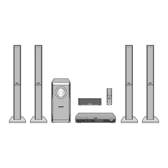
DVD Home Theater Sound System
SA-HT895GC
SA-HT895GCS
SA-HT895GS
Colour
(S).......................Silver Type
At 1kHz and total harmonic of 1%
lFront:
lCenter:
lSurround:
At 100Hz and total harmonic of 1%
lSubwoofer:
lFM tuner section (FM)
Preset Memory:
Frequency Range:
Sensitivity:
S/N 26dB
Antenna terminals:
lAM tuner section (AM/ MW)
Frequency Range:
AM Sensitivity S/N 20dB at
999kHz:
lPhone jack:
© 2006 Panasonic AVC Networks Singapore Pte.
Ltd. All rights reserved. Unauthorized copying and
distribution is a violation of law.
ORDER NO.MD0604126C3
75 W/ Channel (3Ω)
75 W/ Channel (6Ω)
70 W/ Channel (3Ω)
75 W/ Channel (6Ω)
FM 15 stations
AM/MW 15 stations
87.50-108.00MHz
(50kHz in step)
2.5µV (IHF)
2.2µV
75Ω (unbalanced)
522-1629kHz (9kHz in step)
520-1630kHz (10kHz in step)
560µV/m
Advertisement

Related Manuals for Panasonic SA-HT895GC


Summary of Contents for Panasonic SA-HT895GC
- Page 1 AM Sensitivity S/N 20dB at 999kHz: DIN Output Power: Dolby Digital Mode: 560µV/m lTotal DIN Dolby Digital mode Power: lPhone jack: 440 W © 2006 Panasonic AVC Networks Singapore Pte. Ltd. All rights reserved. Unauthorized copying and distribution is a violation of law.
- Page 2 (Sub sampling is 4:0:0, 4:2:0, 4:2:2, 4:4:4). Extremely approx 0.65W long and narrow pictures may not be displayed. Note: *4 MPEG4 data recorded with Panasonic SD multi cameras or DVD video recorders. 1. Specifications are subject to change without notice. lConforming to SD VIDEO specifications (ASF standard)/ Mass and dimensions are approximate.
- Page 3 SA-HT895GC / SA-HT895GCS / SA-HT895GS CONTENTS Page Page 1 Safety Precautions 2 Prevention of Electro Static Discharge (ESD) to 1.1. GENERAL GUIDELINES Electrostatically Sensitive (ES) Devices 1.2. Before Repair and Adjustment 3 Precaution of Laser Diode 1.3. Protection Circuitry 4 About Lead Free Solder (PbF)
- Page 4 SA-HT895GC / SA-HT895GCS / SA-HT895GS 5 Caution for AC Cord (For GS only) 14 Measurements and Adjustments 6 Handling Precautions for Traverse Unit 14.1. Service Tools and Equipment 6.1. Cautions to Be Taken in Handling the Optical Pickup Unit 14.2. Important points in adjustment 14.3.
- Page 5 SA-HT895GC / SA-HT895GCS / SA-HT895GS 1 Safety Precautions 1.1. GENERAL GUIDELINES 1. When servicing, observe the original lead dress. If a short circuit is found, replace all parts which have been overheated or damaged by the short circuit. 2. After servicing, see to it that all the protective devices such as insulation barriers, insulation papers shields are properly installed.
- Page 6 SA-HT895GC / SA-HT895GCS / SA-HT895GS If this occurs, follow the procedure outlines below: 1. Turn off the power. 2. Determine the cause of the problem and correct it. 3. Turn on the power once again after one minute. Note: When the protection circuitry functions, the unit will not operate unless the power is first turned off and then on again.
- Page 7 SA-HT895GC / SA-HT895GCS / SA-HT895GS 3 Precaution of Laser Diode CAUTION : This product utilizers a class 1 laser. Invisible laser radiation is emitted from the optical pick up lens. When the unit is turned on: Wavelength : 658nm/780nm Maximum output radiation power from pick up : 100µW/VDE Laser radiation from pick up unit is safety level, but be sure the followings: 1.
- Page 8 SA-HT895GC / SA-HT895GCS / SA-HT895GS 4 About Lead Free Solder (PbF) 4.1. Service caution based on legal restrictions 4.1.1. General description about Lead Free Solder (PbF) The lead free solder has been used in the mounting process of all electrical components on the printed circuit boards used for this equipment in considering the globally environmental conservation.
- Page 9 SA-HT895GC / SA-HT895GCS / SA-HT895GS 5 Caution for AC Cord (For GS only)
- Page 10 SA-HT895GC / SA-HT895GCS / SA-HT895GS 6 Handling Precautions for Traverse Unit The laser diode in the optical pickup unit may break down due to static electricity of clothes or human body. Special care must be taken avoid caution to electrostatic breakdown when servicing and handling the laser diode.
- Page 11 SA-HT895GC / SA-HT895GCS / SA-HT895GS...
- Page 12 SA-HT895GC / SA-HT895GCS / SA-HT895GS 7 Accessories AC cord Remote control AM loop antenna AC cord (For GS area) FM indoor antenna Speaker cable Video cable Speaker label...
- Page 13 SA-HT895GC / SA-HT895GCS / SA-HT895GS 8 Operation Procedures 8.1. Remote Control Key Buttons Operations...
- Page 14 SA-HT895GC / SA-HT895GCS / SA-HT895GS 8.2. Main Unit Key Buttons Operations...
- Page 15 SA-HT895GC / SA-HT895GCS / SA-HT895GS 8.3. Use of HDAVI Control...
- Page 16 SA-HT895GC / SA-HT895GCS / SA-HT895GS 8.4. Using of Music Port...
- Page 17 SA-HT895GC / SA-HT895GCS / SA-HT895GS 8.5. Disc Information 8.5.1. Disc Playability (Media)
- Page 18 SA-HT895GC / SA-HT895GCS / SA-HT895GS 8.5.2. File Extension Type Support (WMA/MP3/JPEG/MPEG4/DivX)
- Page 19 SA-HT895GC / SA-HT895GCS / SA-HT895GS 8.6. About DivX VOD Content...
- Page 20 SA-HT895GC / SA-HT895GCS / SA-HT895GS 9 New Features 9.1. About HDMI 9.1.1. What is HDMI? 9.1.2. Advanced Digital Pictures...
- Page 21 SA-HT895GC / SA-HT895GCS / SA-HT895GS 9.1.3. Advanced Digital Sound 9.1.4. Easy to Use 9.1.5. HDMI Compatible Products...
- Page 22 SA-HT895GC / SA-HT895GCS / SA-HT895GS 10 Self-Diagnosis and special mode setting 10.1. Service Mode Summary Table The service modes can be activated by pressing various button combination on the player and remote control unit. Below is the summary of major checking:...
- Page 23 SA-HT895GC / SA-HT895GCS / SA-HT895GS 10.2.1. Service Mode Table 1 Item Key Operation FL Display Mode Name Description Front Key Jitter check Jitter check In STOP (no disc) mode, Jitter rate is measured and displayed. press STOP button on the Measurement is repeatedly done in player, and "5"...
- Page 24 SA-HT895GC / SA-HT895GCS / SA-HT895GS 10.2.2. Service Mode Table 2 Item Key Operation FL Display Mode Name Description Front Key Micro-processor Micro-processor firmware version In STOP (no disc) firmware version display & EEPROM checksum display. mode, press STOP button display &...
- Page 25 SA-HT895GC / SA-HT895GCS / SA-HT895GS 10.2.3. Service Mode Table 3 Item Key Operation FL Display Mode Name Description Front Key In STOP (no disc) Timer 1 check Timer 1 check mode, press STOP button Laser operation timer is measured on the player, and "...
- Page 26 SA-HT895GC / SA-HT895GCS / SA-HT895GS...
- Page 27 SA-HT895GC / SA-HT895GCS / SA-HT895GS 10.3. DVD Self Diagnostic Function-Error Code 10.3.1. Error Code Table 1 Error Diagnosis Contents Description of error Automatic FL Display Remarks Code Focus servo error Focus coil NG (OPU unit abnormal) Press [ n STOP] on main unit for next error.
- Page 28 SA-HT895GC / SA-HT895GCS / SA-HT895GS 10.3.2. Error Code Table 2 Error Diagnosis Contents Description of error Automatic FL Display Remarks Code F506 Invalid media Disc is flipped over, TOC unreadable, Press [ n STOP] on main incompatible disc media unit for next error...
- Page 29 SA-HT895GC / SA-HT895GCS / SA-HT895GS 10.3.3. Error Code Table 3 Error Diagnosis Contents Description of error Automatic FL Display Remarks Code F880 Task number is not Message coming from a non-existing Press [ n STOP] on main appropriate task unit for next error...
- Page 30 SA-HT895GC / SA-HT895GCS / SA-HT895GS the lock function mode is entered. · Prohibiting operation of selector and disk 1. Select the DVD/CD function. 2. Press and hold down the button and the power button on the player for at least three seconds. (The message, “___LOCKED_”...
- Page 31 SA-HT895GC / SA-HT895GCS / SA-HT895GS 4. FL will display “RESET” before FL display will change to TOC reading again. 5. Power off unit. Unplug the AC cord. 6. Power on the unit. It should be no problem. If problem persist check on the DVD module P.C.B. or FLASH ROM IC.
- Page 32 SA-HT895GC / SA-HT895GCS / SA-HT895GS 11 Assembling and Disassembling “ATTENTION SERVICER” Be careful when disassembling and servicing. Some chassis components may have sharp edges. Special Note: 1. This section describes the disassembly procedures for all the major printed circuit boards and main components.
- Page 33 SA-HT895GC / SA-HT895GCS / SA-HT895GS 11.1. Disassembly Flow Chart...
- Page 34 SA-HT895GC / SA-HT895GCS / SA-HT895GS 11.2. Main Components and P.C.B. Locations...
- Page 35 SA-HT895GC / SA-HT895GCS / SA-HT895GS 11.3. Disassembly of Top Cabinet Step 1 Remove 4 screws. Step 2 Remove 3 screws. (Rear view) Step 3 Lift up and remove the top cabinet. 11.4. Disassembly of the DVD Lid (When taking out disc manually) ·...
- Page 36 SA-HT895GC / SA-HT895GCS / SA-HT895GS 11.5. Disassembly of Front Panel Assembly · Follow Item 11.3. Step 1 Remove the DVD lid. Step 2 Detach FFC cables at connectors. (CN2006, CN2007, Step 5 Remove the front panel assembly. CN2017) Special Note: Avoid placing the set in a position that might Step 3 Remove 1 screw.
- Page 37 SA-HT895GC / SA-HT895GCS / SA-HT895GS Step 6 Remove 6 screws. Step 7 Remove FL P.C.B., Top Button P.C.B. & Mic P.C.B. 11.8. Disassembly of Relay P.C.B. · Follow Item 11.7. Step 1 Remove 4 screws. Step 2 Detach FFC cables at the connectors. (FP8001, FP8002, FP8003, FP8004) Step 3 Remove Relay P.C.B.
- Page 38 SA-HT895GC / SA-HT895GCS / SA-HT895GS 11.11. Disassembly of Main P.C.B., AC-Inlet P.C.B., Tuner Extent P.C.B. & Voltage Selector P.C.B. · Follow Item 11.3. · Follow (Step 1) to (Step 5) of Item 11.5. · Follow (Step 1) to (Step 4) of Item 11.9.
- Page 39 SA-HT895GC / SA-HT895GCS / SA-HT895GS Step 1 Desolder all pins of IC5701. 11.13. Disassembly of Digital Amp IC Step 2 Desolder 2 pins of Switch Regulator IC. (IC5400) Step 3 Remove the Switch Regulator IC. · Follow (Step 1) to (Step 2) of Item 11.11.
- Page 40 SA-HT895GC / SA-HT895GCS / SA-HT895GS 12 Service Position 12.1. Servicing position of the HDMI Module P.C.B. · Follow Item 11.7. · Follow (Step 1) to (Step 2) of Item 11.8. · Follow (Step 1) to (Step 2) of Item 11.9.
- Page 41 SA-HT895GC / SA-HT895GCS / SA-HT895GS 13 Assembly and Step 4 Remove the traverse unit. disassembly of Mechanism Unit 13.1. Disassembly Procedure 13.1.2. Disassembly of Tray Unit Step 1 Slide the guide tray unit while pressing the stopper in the arrow direction, and remove the guide tray unit.
- Page 42 SA-HT895GC / SA-HT895GCS / SA-HT895GS Step 3 Hook the drive arm concave phase over the tray and Step 4 Spread the tabs at the both sides and pull the tray out. the tray slider. (The tray slides a little forword and stops.).
- Page 43 SA-HT895GC / SA-HT895GCS / SA-HT895GS Step 7 Turn the change lever in the arrow direction till it stops. Step 8 Hook the change lever spring on the change lever project part temporarily. Step 2 Hook the lock lever spring on the lock lever projection part temporarly.
- Page 44 SA-HT895GC / SA-HT895GCS / SA-HT895GS 13.1.4. Disassembly of Tray Loading P.C.B. Step 1 Remove 3 screws Step 2 Remove 4 pins. 13.1.5. Disassembly of Optical Pickup Unit Special Note: Anti-static measures are necessary due to handling of OPU unit .
- Page 45 SA-HT895GC / SA-HT895GCS / SA-HT895GS Step 7 Remove 1 screw. Step 8 Slide the shaft in the arrow direction. Step 4 Remove the optical pickup unit in the arrow direction till it stops. Step 9 Lift the optical pickup unit with the shaft.
- Page 46 SA-HT895GC / SA-HT895GCS / SA-HT895GS (Assembling the optical pickup unit) Step 1 Pass the intermediate FPC through the frame hole. Step 2 Align the guide section of the optical pickup unit with the rail. Step 3 Install the shaft top to the holder.
- Page 47 SA-HT895GC / SA-HT895GCS / SA-HT895GS 14 Measurements and Adjustments 14.1. Service Tools and Equipment Application Name Number Tilt adjustment DVD test disc DVDT-S20 [SPG] TORX screw driver (T6) Available on sales route. (T6) or RFKZ0185 [SPG] Others Grease RFKXPG641 [SPG]...
- Page 48 SA-HT895GC / SA-HT895GCS / SA-HT895GS 14.4. Optical adjustment 14.4.1. Optical pickup tilt adjustment Measurement point Adjustment point Mode Disc Tangential adjustment screw T01 (inner periphery) play DVDT-S20 [SPG] Tilt adjustment screw T30 (center periphery) T43 (outer periphery) play Measuring equipment Adjustment value None (Main unit display for servicing is used.)
- Page 49 SA-HT895GC / SA-HT895GCS / SA-HT895GS 15 Abbreviations INITIAL/LOGO ABBREVIATIONS ERROR TORQUE CONTROL ERROR TORQUE CONTROL INITIAL/LOGO ABBREVIATIONS REFERENCE A0~UP ADDRESS ENCSEL ENCODER SELECT ACLK AUDIO CLOCK ETMCLK EXTERNAL M CLOCK (81MHz/40.5MHz) AD0~UP ADDRESS BUS ETSCLK EXTERNAL S CLOCK (54MHz) ADATA...
- Page 50 SA-HT895GC / SA-HT895GCS / SA-HT895GS INITIAL/LOGO ABBREVIATIONS INITIAL/LOGO ABBREVIATIONS READ ENABLE VBLANK V BLANKING RFENV RF ENVELOPE COLLECTOR POWER SUPPLY RF PHASE DIFFERENCE OUTPUT VOLTAGE (CD-ROM) REGISTER SELECT VCDCONT VIDEO CD CONTROL (TRACKING RSEL RF POLARITY SELECT BALANCE) RESET DRAIN POWER SUPPLY VOLTAGE...
- Page 51 SA-HT895GC / SA-HT895GCS / SA-HT895GS 16 Voltage and Waveform Chart 16.1. HDMI Module P.C.B. IC3701 Re f No. MODE CD P LAY IC3701 Re f No. MODE CD P LAY IC3701 Re f No. MODE CD P LAY Re f No.
- Page 52 SA-HT895GC / SA-HT895GCS / SA-HT895GS IC8151 Re f No. MODE CD P LAY IC8251 Re f No. MODE CD P LAY IC8251 Re f No. MODE CD P LAY IC8421 Re f No. MODE CD P LAY IC8421 Re f No.
- Page 53 SA-HT895GC / SA-HT895GCS / SA-HT895GS 16.2. Main P.C.B. Re f No. IC2004 MODE CD P LAY S TANDBY Re f No. IC2018 MODE CD P LAY S TANDBY Re f No. IC2018 MODE CD P LAY S TANDBY Re f No.
- Page 54 SA-HT895GC / SA-HT895GCS / SA-HT895GS IC5000 Re f No. MODE CD P LAY 29.2 -29.2 -21.2 29.5 -3.4 -29.4 -16.8 -29.2 -3.4 29.5 -29.2 -29.2 29.2 S TANDBY 29.2 -29.2 -21.2 29.2 -3.4 -29.4 -16.8 -29.4 -3.4 29.5 -29.2 -29.2 29.2...
- Page 55 SA-HT895GC / SA-HT895GCS / SA-HT895GS 16.4. Waveform Chart WF No. IC2102-15 (PLAY) WF No. IC2102-16, 17, 18, WF No. IC2102-20 (PLAY) 19, 28, 41, 44 (PLAY) 0.34Vp-p(2usec/div) 88Vp-p(5msec/div) 1Vp-p(500usec/div) 84Vp-p(5msec/div) WF No. IC2102-30 (PLAY) 0.30Vp-p(2usec/div) 4.4Vp-p(5msec/div) 0.28Vp-p(2usec/div) 0.32Vp-p(2usec/div) WF No. IC2102-81 (PLAY) WF No.
- Page 56 SA-HT895GC / SA-HT895GCS / SA-HT895GS WF No. IC3901- 8, 9 (PLAY) WF No. IC3901- 29, 30, 32 WF No. IC3901- 44 (PLAY) WF No. IC3901- 26,27 (PLAY) 33, 35, 36(PLAY) 0.16Vp-p(100nsec/div) 1.4Vp-p(5msec/div) 6.4Vp-p(5msec/div) 12.8Vp-p(5msec/div) WF No. IC3901- 49, 50, 51, 52, WF No.
- Page 57 SA-HT895GC / SA-HT895GCS / SA-HT895GS 17 Illustration of IC's, Transistors and Diodes RFKWMHA03160 C0HBB0000057 (44p) C0ABBA000168 (8p) C0JBAB000011 (14p) (For GCS) C0ABBB000230 (8p) C0JBAR000326 (16p) C1AB00002239 (80p) RFKWMHA02160 C0ABCB000088 (14p) C1AB00001731 (6p) (For GC/GS) C1BB00001098 (100p) C0CBCAD00082 (8p) C3ABPG000133 (54p) C2CBYY000196 (100p) No.1...
- Page 58 SA-HT895GC / SA-HT895GCS / SA-HT895GS...
- Page 59 SA-HT895GC / SA-HT895GCS / SA-HT895GS 18 Wiring Connection Diagram TO FAN UNIT TO FAN UNIT VOLUME CN6901 CN5711 VR6800 H6901 FL P.C.B. CN5704 (SOLDER SIDE) JK6801 HEADPHONE CN5714 SBLU JK5400 P5701 SUBWOOFER TOP BUTTON P.C.B. H6902 AC-IN (SOLDER SIDE) AC-INLET P.C.B.
- Page 60 SA-HT895GC / SA-HT895GCS / SA-HT895GS...
- Page 61 SA-HT895GC / SA-HT895GCS / SA-HT895GS 19 Block Diagram IC8001 IC8251 MN2DS0009AP C0GBG0000048 OPTICAL PICK UP UNIT DV3.2 LSI TRACKING COIL/FOCUS COIL/TRAVERSE/SPINDLE MOTOR DRIVE PHOTO DETECTOR VIN1 VOL4+ VIN2 TRAVERSE VIN3 HEAD MOTOR VIN4 LEVEL VOL4- SHIFT VIN8 BIAS1 VIN7 VHALF...
- Page 62 SA-HT895GC / SA-HT895GCS / SA-HT895GS IC8051 IC8001 C3ABPG000133 MN2DS0009AP 64M SDRAM DV3.2 LSI DAC4 OUT DAC5 OUT Y/PY/G Y/PY/G DAC1 OUT CB/PB/B CB/PB/B DAC2 OUT MEMORY MEMORY CR/PR/R CR/PR/R ADDRESS ADDRESS DAC3 OUT 12bit 12bit SR CK LR CK AD OUT0...
- Page 63 SA-HT895GC / SA-HT895GCS / SA-HT895GS TUNER PACK AM ANT FM ANT IC2801 C9ZB00000461 VIDEO DRIVE IC2802 MIXER IF AMP C1AB00001731 VIDEO BUFFER COIL COIL RF AMP BIAS BUFFER Y/PY/G CY IN 12 MHz CY OUT JK2001 CLAMP Y(RED) CY SAG...
- Page 64 SA-HT895GC / SA-HT895GCS / SA-HT895GS TUNER L(R) IC2104, IC2205 C0ABCB000088 OPERATIONAL AMP IC2102 IC2301 C1BB00001098 ASP(INPUT SELECT/DIGITAL SOUND PROCESSOR/ELECTRONIC VOLUME/TONE) C0JBAR000326 SWITCHING IC8421 Q2305,2306 C0FBBK000050 100(99) Q2303, 2304 24 BIT AUDIO DIGITAL TO ANALOG CONVERTER BUFFER INL5 88(87) (INR5) TONE...
- Page 65 SA-HT895GC / SA-HT895GCS / SA-HT895GS IC5200 IC5000 C1BA00000407 C1BA00000407 AUDIO DIGITAL POWER AMP AUDIO DIGITAL POWER AMP BOOT1 BOOT1 FRONT L CENTER IN1M RELEASE1 IN1M RELEASE1 DRIVER DRIVER INPUT INPUT HIGH HIGH SWITCH1 MODULATOR SWITCH1 IN1P STAGE MODULATOR IN1P STAGE...
- Page 66 SA-HT895GC / SA-HT895GCS / SA-HT895GS IC2105 JK6804 C0ABCB000088 F-MORT-LCH MUSICPORT AMP MUSIC PORT 2(6) 1(7) 3(5) CN2003 RF DATA ROLE CHANGE WIRELSS RCH WIRELSS LCH RF PCONT RF PCONT WIRELSS RF LINK LINK RF DET RF DETECT JK6801 PHONES JK5400...
- Page 67 SA-HT895GC / SA-HT895GCS / SA-HT895GS SIGNAL LINES IC5721 C0DABYY00002 T5721 SWITCHING REGULATOR : MAIN SIGNAL LINE : AM SIGNAL LINE : DVD AUDIO SIGNAL LINE : FM SIGNA L LINE : AM OSC SIGNAL LINE : DVD VIDEO SIGNAL LINE...
- Page 68 SA-HT895GC / SA-HT895GCS / SA-HT895GS...
- Page 69 SA-HT895GC / SA-HT895GCS / SA-HT895GS 20 Schematic Diagram Notes · This schematic diagram may be modified at any time with the development of new technology. Notes: S6800: Tray open / close switch ( Open / Close). S6801: Stop and TUNE mode /FM mode switch ( TUNE MODE/FM MODE).
- Page 70 SA-HT895GC / SA-HT895GCS / SA-HT895GS...
- Page 71 SA-HT895GC / SA-HT895GCS / SA-HT895GS 21 Schematic Diagram 21.1. (A) HDMI Module & Optical Pickup Unit Circuit SCHEMATIC DIAGRAM-1 :+B SIGNAL LINE : CD-DA (AUDIO/VIDEO) SIGNAL LINE OPTICAL PICKUP UNIT CIRCUIT J0JBC0000105 J0JBC0000105 HFM PCB TO ACT GND (IM) DELAY CIRCUIT...
- Page 72 SA-HT895GC / SA-HT895GCS / SA-HT895GS SCHEMATIC DIAGRAM-2 HDMI MODULE CIRCUIT (D2) :MAIN SIGNAL LINE :DVD(VIDEO) SIGNAL LINE :DVD(AUDIO) SIGNAL LINE :+B SIGNAL LINE FL8421 F1H0J1050018 FP8101 VGND Y/PY/G LB8303 J0JBC0000042 Y_PY_G VGND CB/PB/B LB8304 J0JBC0000042 CB_PB_B IC3931 VGND C0JBAA000344 IC8691...
- Page 73 SA-HT895GC / SA-HT895GCS / SA-HT895GS SCHEMATIC DIAGRAM-3 HDMI MODULE CIRCUIT (D2) :+B SIGNAL LINE IC8601 C0EBA0000029 RESET RX8017 D1H88204A024 MA_3 MA_4 MA_2 MA_5 RX8016 IC8651 D1H88204A024 RFKWMHA02160 (GC/GS) MA_1 RFKWMHA03160 (GCS) MA_6 MA_0 16M FLASHROM MA_7 RX8015 IC8606 D1H88204A024 C0EBE0000455...
- Page 74 SA-HT895GC / SA-HT895GCS / SA-HT895GS SCHEMATIC DIAGRAM-4 HDMI MODULE CIRCUIT (D2) :CD-DA SIGNAL LINE :DVD(VIDEO) SIGNAL LINE :DVD(AUDIO) SIGNAL LINE :+B SIGNAL LINE VDD12 LB8001 J0JHC0000045 LB8011 J0JHC0000045 D+3.3V TRCDATA3 TRCDATA2 RX8031 D1H447220001 TRCDATA1 MDQ18 TRCDATA1 TRCDATA0 TRCDATA0 R8041 TRCCLK...
- Page 75 SA-HT895GC / SA-HT895GCS / SA-HT895GS SCHEMATIC DIAGRAM-5 HDMI MODULE CIRCUIT (D2) :CD-DA SIGNAL LINE :DVD(VIDEO) SIGNAL LINE :+B SIGNAL LINE DRV0 OSC27M OSC27M R8230 2.2K DRV1 K8325 DAC5OUT R8568 IC8251 Q8562 C0GBG0000048 B1ADGB000008 MOTOR DRIVER R8564 LD DRIVE RX8032 D1H447220001...
- Page 76 SA-HT895GC / SA-HT895GCS / SA-HT895GS SCHEMATIC DIAGRAM-6 HDMI MODULE CIRCUIT (UP) :DVD(VIDEO) SIGNAL LINE :+B SIGNAL LINE RX3705 D1H81014A024 CBCROUT_7 CBCROUT_6 CBCROUT_5 CBCROUT_4 RX3704 D1H81014A024 CBCROUT_3 CBCROUT_2 CBCROUT_1 LB3701 J0JHC0000045 CBCROUT_0 RX3703 D1H81014A024 YOUT_7 99 98 97 96 95 94...
- Page 77 SA-HT895GC / SA-HT895GCS / SA-HT895GS SCHEMATIC DIAGRAM-7 HDMI MODULE CIRCUIT (HD) :DVD(VIDEO) SIGNAL LINE :DVD(AUDIO) SIGNAL LINE :MAIN SIGNAL LINE :+B SIGNAL LINE CBCROUT_7 I2C_SDA CBCROUT_6 I2C_SCL CBCROUT_5 TXRST CBCROUT_4 CBCROUT_3 CBCROUT_2 CBCROUT_1 CBCROUT_0 LB3902 C3902 J0JHC0000045 4V 330 L3903...
- Page 78 SA-HT895GC / SA-HT895GCS / SA-HT895GS 21.2. (B) Main Circuit SCHEMATIC DIAGRAM-8 MAIN CIRCUIT :+B SIGNAL LINE :-B SIGNAL LINE : AUX SIGNAL LINE : MUSIC PORT SIGNAL LINE : DVD VIDEO SIGNAL LINE CN2001 STATUS DVD_STA DVD_CMD DSPCLK DVD_CK F_MPORT-RCH...
- Page 79 SA-HT895GC / SA-HT895GCS / SA-HT895GS SCHEMATIC DIAGRAM-9 MAIN CIRCUIT :+B SIGNAL LINE R2053 R2051 R2061 R2063 R2066 2.2K RGB_H YC_H R2067 YC_H W2500 0 ASP_CK R2068 ASP_CLK ASP_DA R2069 R2014 ASP_DAT FLD_CLK R2070 R2083 VIDEO_MUTE FLD_CLK VIDEO_MUTE IC2004 FLD_STB R2071...
- Page 80 SA-HT895GC / SA-HT895GCS / SA-HT895GS SCHEMATIC DIAGRAM-10 MAIN CIRCUIT :+B SIGNAL LINE : MAIN SIGNAL LINE : AUX SIGNAL LINE : FM /AM SIGNAL LINE : MUSIC PORT SIGNAL LINE :-B SIGNAL LINE C2024 220P C2023 220P R2307 1.8K R2407 1.8K...
- Page 81 SA-HT895GC / SA-HT895GCS / SA-HT895GS SCHEMATIC DIAGRAM-11 MAIN CIRCUIT :+B SIGNAL LINE :-B SIGNAL LINE : MAIN SIGNAL LINE C2325 R2334 R2333 C2425 R2434 R2433 0.047 0.047 R2443 R2343 R2335 R2435 W2530 W2536 W2526 R2188 2.2K FLFIN C2328 R2314 R2315...
- Page 82 SA-HT895GC / SA-HT895GCS / SA-HT895GS SCHEMATIC DIAGRAM-12 MAIN CIRCUIT :+B SIGNAL LINE :-B SIGNAL LINE : MAIN SIGNAL LINE : MUSIC PORT SIGNAL LINE : DVD VIDEO SIGNAL LINE Q2912 C2324 2700P B1BACD000018 R2976 L2910 +12V REGULATOR G0C220JA0055 TUN+9V C2183 1...
- Page 83 SA-HT895GC / SA-HT895GCS / SA-HT895GS 21.3. (C) Power, AC-inlet & Voltage Selector Circuit SCHEMATIC DIAGRAM-13 POWER(DIGITAL AMP) CIRCUIT : MAIN SIGNAL LINE :+B SIGNAL LINE :-B SIGNAL LINE C5002 R5000 R5501 R5505 5.6K 100K IC5500 IN+_FL HOP_DA FRONT FL C0JBAB000011...
- Page 84 SA-HT895GC / SA-HT895GCS / SA-HT895GS SCHEMATIC DIAGRAM-14 POWER(DIGITAL AMP) CIRCUIT :+B SIGNAL LINE :-B SIGNAL LINE : MAIN SIGNAL LINE IC5200 C1BA00000407 AUDIO DIGITAL POWER AMP IN-_C IN+_C C5215 C5210 C5203 C5205 220P 220P C5218 220P R5210 VDDP IC5400 C1BA00000407...
- Page 85 SA-HT895GC / SA-HT895GCS / SA-HT895GS SCHEMATIC DIAGRAM-15 POWER(SMPS) CIRCUIT :+B SIGNAL LINE :-B SIGNAL LINE Q5740 R5745 B1BACG000048 0(GC) Q5752 4.7(GCS/GS) FAN MOTOR DRIVE DC_18V B1ABCF000176 C5770 FAN MOTOR DRIVE 0.01 Q5742 B1ABCF000176 R5739 R5767 D5711 FAN MOTOR DRIVE 1.2K...
- Page 86 SA-HT895GC / SA-HT895GCS / SA-HT895GS SCHEMATIC DIAGRAM-16 VOLTAGE SELECTOR CIRCUIT POWER(SMPS) CIRCUIT :+B SIGNAL LINE S5000 VOLTAGE SELECTOR D5701 TH5702 B0FBAR000018 D4CAC8R00002 SBLU 110-127V D5707 D5705 (GC) 220-240V B0BC035A0007 B0EAMM000057 R5707 R5706 Q5701 D5702 2SC3940ARA B0ZAZ0000052 L5704 CURRENT LIMMITTING Q5747...
- Page 87 SA-HT895GC / SA-HT895GCS / SA-HT895GS 21.4. (D) FL, Top Button, Mic, Music Port, Tuner Extent, Tray Loading & Relay Circuit SCHEMATIC DIAGRAM-17 FL CIRCUIT :+B SIGNAL LINE :-B SIGNAL LINE : MAIN SIGNAL LINE FL6901 A2BD00000160 FL DISPLAY 2 3 4 5 6 7 8 9 10 11...
- Page 88 KEY1 R6949 L6904 DAP_LCH J0JBC0000019 DAP_GND(AGND) DAP_RCH DAP_GND(ANG) MAIN R6948 D6900 CIRCUIT R6905 DGND B3AAA0000803 (CN2006) on W6901 STBLED W601 SCHEMATIC VREF DIAGRAM- 12 W6904 W6910 W6906 W6999 SW5V W602 SA-HT895GC/GS/GCS TUNER EXTENT/ MUSIC PORT/ TRAY LOADING/ MIC/ RELAY CIRCUIT...
- Page 89 SA-HT895GC / SA-HT895GCS / SA-HT895GS 22 Printed Circuit Board 22.1. (A) HDMI Module P.C.B. HDMI MODULE P.C.B. (REP4034D...GC/GS,REP4034E...GCS) FP3902 FP8101 C8424 FL8104 FL8102 1 2 3 4 5 6 FL8421 C8423 C8421 LB8692 IC8695 IC8151 C8055 QR8420 2 3 4 5...
- Page 90 SA-HT895GC / SA-HT895GCS / SA-HT895GS 22.2. (B) Main/ Power P.C.B. MAIN/POWER P.C.B. (REPX0507A...GC,REPX0507B...GS,REPX0507C...GCS) PC5701 IC5702 (GCS/GS) D5703 LB5704 CN5711 R5763 R5708 C5761 1 2 3 4 IC5701 D5704 R5703 C5720 D5772 R5704 R5713 D5706 W5730 Q5752 D5702 R5767 Q5747 L5501...
- Page 91 S6805 S6800 C6923 W6904 C6918 (FORWARD) (REVERSE) (OPEN/CLOSE) R6934 W601 W6903 W6902 W602 0479A-1 0479A-1 R6829 R6926 R6927 D6900 S6807 S6806 (WIDE SURR) C6922 (POWER) R6925 R6928 H6902 Z6900 JK6804 CN6902 SENSOR MUSIC PORT SA-HT895GC/GS/GCS TUNER EXTENT/AC-INLET/FL/MUSIC PORT/TOP BUTTON P.C.B.
- Page 92 SA-HT895GC / SA-HT895GCS / SA-HT895GS 22.4. (D) Mic , Tray Loading, Relay & Voltage Selector P.C.B. MIC P.C.B. (REPX0539A...GC/GS, TRAY LOADING P.C.B. (REP3288B) REPX0539E...GCS) (LOADING IC904 MOTOR) C6703 R6710 R6709 R6706 H6903 R6702 W6701 S902 C6702 R6705 CS901 (OPEN SW)
- Page 93 SA-HT895GC / SA-HT895GCS / SA-HT895GS 23 Basic Troubleshooting Guide 23.1. Basic Troubleshooting Guide for Traverse Unit (HDMI Module P.C.B) Problems Checking Points Checking components 1) Distorted picture or abnormal a) Check SDRAM address, data bus, CLK and IC8051 sound is heard during initialisation...
- Page 94 SA-HT895GC / SA-HT895GCS / SA-HT895GS 23.2. Basic Troubleshooting Guide for HDMI AV output Problems Checking Points Checking components 1) TV does not have display. Set 1) Check setting of the set in Setup Menu whether FL display shows U702 / U703.
- Page 95 SA-HT895GC / SA-HT895GCS / SA-HT895GS 24 Overall Block (HT895)
- Page 96 SA-HT895GC / SA-HT895GCS / SA-HT895GS 24.1. HT895 DVD Unit Block...
- Page 97 SA-HT895GC / SA-HT895GCS / SA-HT895GS 24.2. HT895 Block (Analog Signal : DVD 5.1ch Play Back Mode)
- Page 98 SA-HT895GC / SA-HT895GCS / SA-HT895GS 24.3. HT895 Block (Analog Signal : 2ch Analog Input Mode)
- Page 99 SA-HT895GC / SA-HT895GCS / SA-HT895GS 24.4. HT895 Power Supply Block...
- Page 100 SA-HT895GC / SA-HT895GCS / SA-HT895GS 24.5. HT895 Power Block (SMPS)
- Page 101 SA-HT895GC / SA-HT895GCS / SA-HT895GS 25 Terminal Function of ICs 25.1. IC2018 (C2CBYY000196): Terminal Name Function Micro-processor IC 48 ASP_DA O ASP data (R2S15203FP) 49 ASP_CK O ASP clock (R2S15203FP) Terminal Name Function 50 MUTE_HP O Headphone mute 51 MP_SEL...
- Page 102 SA-HT895GC / SA-HT895GCS / SA-HT895GS 26 Exploded Views 26.1. Cabinet Parts Location...
- Page 103 SA-HT895GC / SA-HT895GCS / SA-HT895GS...
- Page 104 SA-HT895GC / SA-HT895GCS / SA-HT895GS 26.2. Packaging...
- Page 105 SA-HT895GC / SA-HT895GCS / SA-HT895GS 27 Replacement Parts List Notes: *Important safety notice: Components identified by mark have special characteristics important for safety purpose. Furthermore, special parts which have purposes of fire-retardant (resistors), high-quality sound (capacitors), low-noise (resistors), etc. are used.
- Page 106 SA-HT895GC / SA-HT895GCS / SA-HT895GS 27.1. Component Parts List Ref. Part No. Part Name & Description Remarks RMM0248 SUB RACK Ref. Part No. Part Name & Description Remarks RMC0387 SUPPORT SPRING RMR1446-X CLAMPER CABINET AND CHASSIS XTN26+6GFJ SCREW XTV2+6GFJ SCREW...
- Page 107 SA-HT895GC / SA-HT895GCS / SA-HT895GS Ref. Part No. Part Name & Description Remarks Ref. Part No. Part Name & Description Remarks IC904 C0GAY0000013 IC MOTOR DRIVER Q3903 B1CFHA000002 TRANSISTOR IC2018 C2CBYY000196 IC MIRCO-PROCESSOR Q3941 2SD1819A0L TRANSISTOR IC2102 C1BB00001098 IC ASP...
- Page 108 SA-HT895GC / SA-HT895GCS / SA-HT895GS Ref. Part No. Part Name & Description Remarks Ref. Part No. Part Name & Description Remarks D5701 B0FBAR000018 DIODE LB8425 ERJ2GE0R00X CHIP RESISTOR D5702 B0ZAZ0000052 DIODE LB8426 ERJ2GE0R00X CHIP RESISTOR D5703 B0BC02900004 DIODE LB8427 ERJ2GE0R00X...
- Page 109 SA-HT895GC / SA-HT895GCS / SA-HT895GS Ref. Part No. Part Name & Description Remarks Ref. Part No. Part Name & Description Remarks COMPONENT COMBINATION FP3902 K1MN06BA0148 6P CONNECTOR FP8001 K1MN06BA0147 6P CONNECTOR Z6900 B3MAZ0000023 R/CONTROL SENSOR FP8002 K1MN06BA0147 6P CONNECTOR FP8003...
- Page 110 SA-HT895GC / SA-HT895GCS / SA-HT895GS Ref. Part No. Part Name & Description Remarks Ref. Part No. Part Name & Description Remarks REEX0449B-1L SPEAKER CORD R2077 ERJ3GEYJ332V 3.3K 1/16W [M]GCS/ XSN5+12FJ SCREW R2078 ERJ3GEYJ472V 4.7K 1/16W R2079 ERJ3GEYJ103V 10K 1/16W RESISTORS...
- Page 111 SA-HT895GC / SA-HT895GCS / SA-HT895GS Ref. Part No. Part Name & Description Remarks Ref. Part No. Part Name & Description Remarks R2269 ERJ3GEYJ104V 100K 1/16W R2422 ERJ3GEYJ472V 4.7K 1/16W R2270 ERJ3GEYJ222V 2.2K 1/16W R2423 ERJ3GEYJ123V 12K 1/16W R2271 ERJ3GEYJ563V 56K 1/16W...
- Page 112 SA-HT895GC / SA-HT895GCS / SA-HT895GS Ref. Part No. Part Name & Description Remarks Ref. Part No. Part Name & Description Remarks R2920 ERJ3GEYJ472V 4.7K 1/16W R5035 ERJ3GEYJ562V 5.6K 1/16W R2921 ERJ3GEYJ151V 150 1/16W [M]GCS/ R5036 ERJ3GEYJ562V 5.6K 1/16W R5037 ERJ3GEYJ562V 5.6K 1/16W...
- Page 113 SA-HT895GC / SA-HT895GCS / SA-HT895GS Ref. Part No. Part Name & Description Remarks Ref. Part No. Part Name & Description Remarks R5726 ERJ3GEYJ102V 1K 1/16W R6706 ERJ3GEYJ102V 1K 1/16W R5727 ERJ3GEYJ222V 2.2K 1/16W R6707 ERJ3GEYJ332V 3.3K 1/16W R5728 ERJ3GEY0R00V 0 1/16W...
- Page 114 SA-HT895GC / SA-HT895GCS / SA-HT895GS Ref. Part No. Part Name & Description Remarks Ref. Part No. Part Name & Description Remarks R8556 ERJ3GEYJ560V 56 1/16W W2511 ERJ3GEY0R00V CHIP JUMPER R8557 ERJ3GEYJ510V 51 1/16W W2513 ERJ3GEY0R00V CHIP JUMPER R8558 ERJ2GEJ473X 47K 2W...
- Page 115 SA-HT895GC / SA-HT895GCS / SA-HT895GS Ref. Part No. Part Name & Description Remarks Ref. Part No. Part Name & Description Remarks W6924 ERJ6GEY0R00V CHIP RESISTOR CHIP RESISTORS W6925 ERJ6GEY0R00V CHIP RESISTOR W6926 ERJ6GEY0R00V CHIP RESISTOR K3702 ERJ3GEY0R00V CHIP JUMPER W6927...
- Page 116 SA-HT895GC / SA-HT895GCS / SA-HT895GS Ref. Part No. Part Name & Description Remarks Ref. Part No. Part Name & Description Remarks C2187 ECJ1VC1H470J 47P 50V C2422 ECJ1VB1A105K 1 10V C2188 ECJ1VC1H101J 100P 50V C2423 ECJ1VB1H471K 470P 50V C2189 ECJ1VB1C104K 0.1 16V...
- Page 117 SA-HT895GC / SA-HT895GCS / SA-HT895GS Ref. Part No. Part Name & Description Remarks Ref. Part No. Part Name & Description Remarks C2903 ECJ1VB1H103K 0.01 50V C3941 ECJ0EB1E271K 270P 25V C2906 ECJ1VB1H103K 0.01 50V C3954 ECJ0EF1C104Z 0.1 16V C2908 ECA1CM221B 220 16V...
- Page 118 SA-HT895GC / SA-HT895GCS / SA-HT895GS Ref. Part No. Part Name & Description Remarks Ref. Part No. Part Name & Description Remarks C5220 ECJ1VB1H104K 0.1 50V C5510 ECA1VM471B 470 35V C5221 ECJ1VB1H102K 1000P 50V C5511 ECA1VM471B 470 35V C5222 ECJ1VB1H104K 0.1 50V...
- Page 119 SA-HT895GC / SA-HT895GCS / SA-HT895GS Ref. Part No. Part Name & Description Remarks Ref. Part No. Part Name & Description Remarks C6701 ECJ1VB1C105K 1 16V C8231 ECJ0EB1A104K 0.1 10V C6702 ECJ1VB1H221K 220P 50V C8232 ECJ0EB1A104K 0.1 10V C6703 ECJ1VC1H470J 47P 50V...
- Page 120 SA-HT895GC / SA-HT895GCS / SA-HT895GS Ref. Part No. Part Name & Description Remarks C8695 ECJ0EF1C104Z 0.1 16V C8701 ECJ0EB1A104K 0.1 10V...
Need help?
Do you have a question about the SA-HT895GC and is the answer not in the manual?
Questions and answers