Table of Contents
Advertisement
Quick Links
Advertisement
Table of Contents

Related Manuals for E-ELEMENTS USB3 HT3

Summary of Contents for E-ELEMENTS USB3 HT3
- Page 1 USB3_HT3 Reference Manual October 2019 ver1.2...
- Page 2 Copyright Notice and Proprietary Information © 2018 E-elements Technology Co., Ltd. These all associated documentation are proprietary to E-elements and may only be used pursuant to the terms and conditions of a written license agreement with E-elements. All other use, reproduction, modification, or distribution of the associated documentation is strictly prohibited.
-
Page 3: Revision History
Revision History Date Comment Apr 2018 Initial version Aug 2019 v1.0 Correct the block diagram Aug 2019 v1.1 Add VBUS mode description Oct 2019 V1.2 Update the Diagram and J6-J12 default value USB3_HT3 Reference anual © 2018 E-elements Tech. August 2019... -
Page 4: Table Of Contents
Card Placement ......................9 Block Diagram ......................10 Modes .......................... 11 VBUS Handling ......................12 Standard VCCO GPIO Headers .................13 Clocks .......................... 15 Pin Tables ........................16 HT3 Connectors ....................16 GPIO Connectors ....................18 USB3_HT3 Reference anual © 2018 E-elements Tech. August 2019... -
Page 5: Usb3_Ht3
When connecting daughter boards and HT3 cable connectors, they should be held parallel to the USB3_HT3 connector throughout the mating process. USB3_HT3 Reference anual © 2018 E-elements Tech. August 2019... -
Page 6: Overview
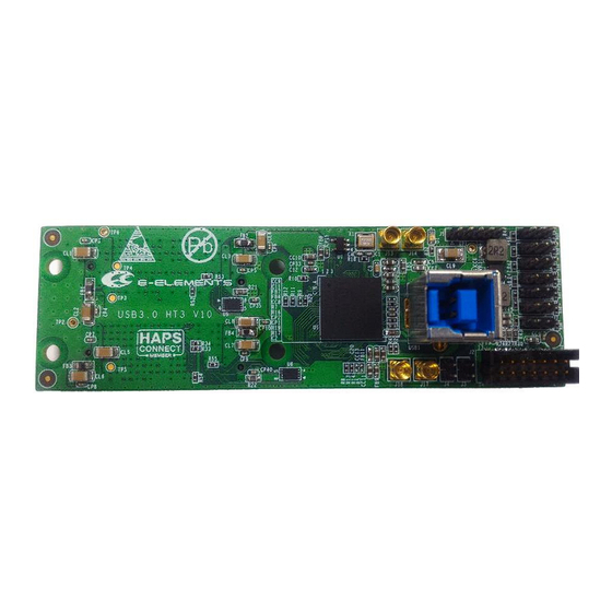
USB 3.0 Type A (F) to Type B (M) adapter is included for host mode. The daughter board provides a ULPI (UTMI + Low Pin) interface for USB 2.0 operation and a PIPE interface for USB 3.0 operation. Figure 1: Top and Bottom View of USB3_HT3 © 2018 E-elements Tech. USB3_HT3 Reference anual August... - Page 7 1 HAPS 14-pin GPIO Headers • 1 HAPS 5-pin GPIO Headers • 1 USB 3.0 Transceiver • 1 USB 3.0 TYPE B Connector • 2 HT3 Connectors • 2 pairs of Differential MMCX Clock Connectors © 2018 E-elements Tech. USB3_HT3 Reference Manual August 2019...
-
Page 8: Layout
Layout USB3_HT3 Layout Figure 2: Top and Bottom(dotted line) USB3_HT3 Card Layout © 2018 E-elements Tech. USB3_HT3 Reference Manual August 2019... -
Page 9: Card Placement
I/O standards can be used for the signal pins. The USB3_HT3 card connected to HAPS-80 through two HT3 connectors, Figure 3 is the example of card installed Figure 3: USB3_HT3 Card Installed on HAPS-80 system © 2018 E-elements Tech. USB3_HT3 Reference Manual August 2019... -
Page 10: Block Diagram
HT3 and USB3.0 connector. The following I/O block diagram in Figure 5 depicts how functional blocks are interconnected. Figure 4: Block Diagram Figure 5: I/O Block Diagram © 2018 E-elements Tech. USB3_HT3 Reference Manual August 2019... -
Page 11: Modes
For device mode disconnect a wire between pins 1 and 2 on J3 and Mode Host short short Device open open Host mode Host mode (Current-limited) Figure 6: USB3 mode configuration © 2018 E-elements Tech. USB3_HT3 Reference Manual August 2019... -
Page 12: Vbus Handling
Local +5 V Local +5 V with Current-limited Table 1: VBUS Source Selection +5V through Local USB cable +5V rail Current-limited FPGA_VBUS_EN_N USB con. Local TPS2560DRC (From HT3 JX1) Figure 7: VBUS Handling © 2018 E-elements Tech. USB3_HT3 Reference Manual August 2019... -
Page 13: Standard Vcco Gpio Headers
Figure 5, on page 10. 1 2 3 Figure 8: Header Strip J6-J12 is populated by jumpers that connect pull-up or pull-down Resistor for the signal directly to HT3 I/O signals and USB3.0. © 2018 E-elements Tech. USB3_HT3 Reference Manual August 2019... - Page 14 PIPE3_PHY_STATUS ULPI_DATA7 ULPI_DATA6 ULPI_DATA5 ULPI_DATA4 VBUS Handling J3-J4 is populated by jumpers that connect VBUS of USB1 to 5V. Refer to the VBUS Handling and in Figure 7, on page 12. © 2018 E-elements Tech. USB3_HT3 Reference Manual August 2019...
-
Page 15: Clocks
MMCX connector. Differential MMCX Source or Destination or Single- ended Direction Connector J13/J14 DIFF Output Source J17/J18 DIFF Output Table 3: MMCX Clock Connections JX1_C0_P JX1_C0_N JX2_C0_P JX2_C0_N Figure 9: DIFF Clocks © 2018 E-elements Tech. USB3_HT3 Reference Manual August 2019... -
Page 16: Pin Tables
Pin Table USB3_HT3 Pin Table HT3 Connectors © 2018 E-elements Tech. USB3_HT3 Reference Manual August 2019... - Page 17 Pin Table USB3_HT3 © 2018 E-elements Tech. USB3_HT3 Reference Manual August 2019...
-
Page 18: Gpio Connectors
Trace Name VBUS DM_ULPI DP_ULPI SSTXN SSTXP SSRXN SSRXP GPIO Connectors Trace Name Trace Name +1V8 JX1_D10 JX1_D11 +1V8 JX1_A9 JX1_D12 JX1_A8 JX2_A12 JX1_D1 JX2_D12 JX1_A12 JX1_D3 JX1_D2 JX1_D5 JX1_D4 JX1_D7 JX1_D6 © 2018 E-elements Tech. USB3_HT3 Reference Manual August 2019...
Need help?
Do you have a question about the USB3 HT3 and is the answer not in the manual?
Questions and answers