Roland OCTAPAD SPD-30 Service Notes
Hide thumbs
Also See for OCTAPAD SPD-30:
- Supplementary manual (4 pages) ,
- Training manual (4 pages) ,
- Owner's manual (80 pages)
Table of Contents
Advertisement
Mar. 2010
Table of Contents
Cautionary Notes ..............................................................2
Specifications .....................................................................3
Location of Controls .........................................................4
Location of Controls Parts List........................................4
Exploded View ..................................................................6
Exploded View Parts List.................................................7
Plain View (1).....................................................................8
Plain View (1) Parts List ...................................................9
Plain View (2)...................................................................10
Plain View (2) Parts List .................................................11
Notes .................................................................................12
Wiring Diagram...............................................................18
Parts List ...........................................................................19
Verifying the Version Numbers....................................21
About the Serial Number ...............................................21
Data Backup and Restore Operations ..........................22
Performing a Factory Reset............................................22
Updating the System ......................................................23
Test Mode .........................................................................24
Copyright © 2010 Roland Corporation
All rights reserved. No part of this publication may be reproduced in any form without the written permission
of Roland Corporation.
Block Diagram .................................................................30
Circuit Board (Main Board) ...........................................32
Circuit Diagram (Main Board: 1/2) ..............................34
Circuit Diagram (Main Board: 2/2) ..............................36
Circuit Board (Jack Board: 1/2).....................................38
Circuit Board (Jack Board: 2/2).....................................40
Circuit Diagram (Jack Board: 1/3)................................42
Circuit Diagram (Jack Board: 2/3)................................44
Circuit Diagram (Jack Board: 3/3)................................46
Circuit Board (Panel Board: 1/2) ..................................48
Circuit Board (Panel Board: 2/2) ..................................50
Circuit Diagram (Panel Board: 1/2) .............................52
Circuit Diagram (Panel Board: 2/2) .............................54
Board)................................................................................56
Circuit Diagram (LED-A Board) ...................................57
Circuit Diagram (LED-B Board)....................................57
Circuit Diagram (LED-C Board) ...................................57
Circuit Diagram (LED-D Board) ...................................57
17058672E0
SERVICE NOTES
Issued by RJA
SPD-30
CC-KWS
Advertisement
Table of Contents

Related Manuals for Roland OCTAPAD SPD-30


Summary of Contents for Roland OCTAPAD SPD-30
-
Page 1: Table Of Contents
Circuit Diagram (LED-C Board) ........57 Updating the System ............23 Circuit Diagram (LED-D Board) ........57 Test Mode .................24 Copyright © 2010 Roland Corporation All rights reserved. No part of this publication may be reproduced in any form without the written permission of Roland Corporation. 17058672E0... -
Page 2: Cautionary Notes
• Because reissuance is restricted. • Because the part is made to order (at current market price). • Because it is carried in electronic data on the Roland web site. • Because it is a package or an accessory irrelevant to the function maintenance of the main body. -
Page 3: Specifications
Connectors * Printed matters will not be supplied after the end of the production. Then, download the electronic file from the Roland web site. PHONES Jack (Stereo 1/4 inch phone type) * In the interest of product improvement, the specifications and/or appearance of OUTPUT Jacks (L (MONO), R) (1/4 inch phone type) this unit are subject to change without prior notice. -
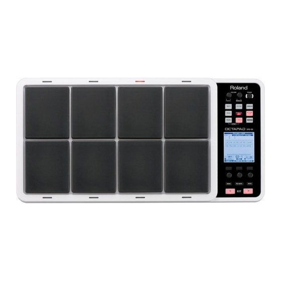
Page 4: Location Of Controls
Mar. 2010 SPD-30 Location of Controls fig.panel.eps Location of Controls Parts List Part Code Part Name Description Q’ty 5100010681 TOP CASE ASSY 5100009444 LED LENS 5100009458 PANEL SHEET 5100009446 ZN R-KNOB MF-ELA BLK 5100009449 RUBBER SW A 5100009451 RUBBER SW B 5100009445 ZN R-KNOB MF-ELA ENC BLK... - Page 5 Mar. 2010 SPD-30...
-
Page 6: Exploded View
Mar. 2010 SPD-30 Exploded View fig.bunakizu-All.eps... -
Page 7: Exploded View Parts List
Mar. 2010 SPD-30 Exploded View Parts List Part Code Part Name Description Q’ty 5100009446 ZN R-KNOB MF-ELA BLK 5100009445 ZN R-KNOB MF-ELA ENC BLK 5100009458 PANEL SHEET 5100010681 TOP CASE ASSY * This unit includes the following parts. ******** TOP CASE TOP CASE ******** PAD ASSY... -
Page 8: Plain View (1)
Mar. 2010 SPD-30 Plain View (1) fig.bunakizu-1.eps View 1 View 2... -
Page 9: Plain View (1) Parts List
Mar. 2010 SPD-30 Plain View (1) Parts List View 1 Part Code Part Name Description Q’ty 40459534 SCREW M3X10 PAN MACHINE W/SW+PW BZC View 2 Part Code Part Name Description Q’ty 5100013786 SCREW 4X12 TRUSS TAPTITE P BZC 5100013787 SCREW 4X16 TRUSS TAPTITE P BZC 40238145 SCREW M5X12... -
Page 10: Plain View (2)
Mar. 2010 SPD-30 Plain View (2) fig.bunakizu-2.eps View 3 View 4 View 5... -
Page 11: Plain View (2) Parts List
Mar. 2010 SPD-30 Plain View (2) Parts List View 3 Part Code Part Name Description Q’ty 40011312 SCREW 3X8 BINDING TAPTITE P FE BZC 40011334 SCREW 3X12 BINDING TAPTITE P FE BZC 40011056 SCREW 3X6 BINDING TAPTITE B ZC View 4 Part Code Part Name Description... -
Page 12: Disassembly/Assembly Procedure And Important Notes
Mar. 2010 SPD-30 Disassembly/Assembly Procedure and Important Notes Detaching the Bottom Case Insert the flat cables (2 locations) into the connectors. fig.bunaki-2.eps While applying pressure in the A direction, lift in the B direction. fig.bunaki-1.eps Lower the Bottom Case in the direction of the arrow. fig.bunaki-4.eps Detach the flat cables (2 locations). - Page 13 Mar. 2010 SPD-30 Bending the Flat Cables Attaching the Gasket fig.bunaki-FFC.eps When replacing the Main Board Assy, attach a Gasket (#5100011928) on JK1. fig.bunaki-gasket.eps How to Bend A fig.bunaki-FFC-A.eps Installing the LED Lens Cut 5-millimeter lengths of double-sided adhesive tape (#5100011185) and affix them to the LED lens (#5100009444).
- Page 14 Mar. 2010 SPD-30 Affixing the LED Cushion Attaching the Dust Covers When replacing the Panel Board Assy, attach an LED Cushion (#5100013049). Dust covers are located on the Panel Board Assy and the underside of the Top Attach so that the silkscreening around LED705 and LED710 remains visible. Case.
- Page 15 Mar. 2010 SPD-30 Dust Covers on the Underside of the Top Installing Components Around the LCD Case Screen Cut 10-millimeter lengths of double-sided adhesive tape (#5100011185), Fasten the Shield Sheet (#5100009465) to the Top Case using screws affix them to the Top Case, and peel off the backing paper. (#40011312).
- Page 16 Mar. 2010 SPD-30 Connector Insertion on the Jack Board Connecting the Sensor Cables When inserting the connector into CN5 on the Jack Board Assy, first place your On the service-use Top Case Assy (#5100010681), the cables extending from 1 hands at the edges of the circuit board, then insert the connector. through 8 in the figure are secured in place using cable ties.
- Page 17 Mar. 2010 SPD-30 Arrange cable 5 as shown in the figure. Using a cable tie, secure cables 1, 5, 2, 6, and C at the hole on the left. fig.bunaki-sensor-4.eps fig.bunaki-sensor-7.eps Using cable ties, secure cables 4 and 8 in place as shown in the figure. Next, use a cable tie to secure in place at the hole on the right.
-
Page 18: Wiring Diagram
Mar. 2010 SPD-30 Wiring Diagram fig.wiring.eps Part Code Part Name Description Q’ty 5100009519 WIRING A-1.0-40X170-4(8)X4(8)-.7X.05 5100009524 WIRING 5100009526 WIRING 5100009525 WIRING * The 16-pin FPC and 2-pin wiring are surface-mounted on the LCD screen. * 2-pin wiring is surface-mounted on PAD1 through 8 and the Cancel Piezo element. -
Page 19: Parts List
Mar. 2010 SPD-30 Parts List fig.-part1-e.eps Due to one or more of the following reasons, Safety Precautions: parts with parts code ******** cannot be supplied as service parts. The parts marked have safety-related characteristics. Use only listed parts for replacement. •... - Page 20 Mar. 2010 SPD-30 SCREWS 40238145 SCREW M5X12 TRUSS BZC 40459534 SCREW M3X10 PAN MACHINE W/SW+PW BZC 40011056 SCREW 3X6 BINDING TAPTITE B ZC 40011312 SCREW 3X8 BINDING TAPTITE P FE BZC 40011334 SCREW 3X12 BINDING TAPTITE-P FE BZC 5100013786 SCREW 4X12 TRUSS TAPTITE BZC 5100013787 SCREW 4X16...
-
Page 21: Verifying The Version Numbers
Knob 1 Knob 2 Knob 2 Knob 3 Knob 3 voltage category are displayed at the bottom right of the Roland logo screen. fig.test1.eps_80 Hold down [QUICK] + [Button 3] + [STANDBY] and switch on the power. Verify the version. -
Page 22: Data Backup And Restore Operations
Mar. 2010 SPD-30 Data Backup and Restore Data Restore Operation Operations The following procedure restores backed-up user settings from a USB memory device to the unit. Insert the USB memory device containing the backed-up user settings into the USB MEMORY connector on the rear panel. For [Knob 1] through [Knob 3] and [Button 1] through [Button 3] Press [MENU]. -
Page 23: Updating The System
Mar. 2010 SPD-30 Updating the System The versions of the update-use files on the USB memory device are displayed. Also, the LEDs corresponding to the respective files light up as shown below. Update-use file Screen display Illuminated LED For the program ROM After performing the update, be sure to execute a factory reset. -
Page 24: Test Mode
Mar. 2010 SPD-30 Test Mode Entering the Test Mode For [Knob 1] through [Knob 3] and [Button 1] through [Button 3] used in the various operations, refer to the figure below. fig.buttons-e.eps At the end of the Test Mode, be sure to execute a factory reset. Executing a factory reset causes kit and phrase data in the unit to be lost. - Page 25 Mar. 2010 SPD-30 1. Version Display [1/15 VERSION] 3. SW (Switch) and LED Test [3/15 SW/LED] fig.test1.eps_80 Verify that all LEDs are dark. Press, in sequence, all buttons other than [POWER], and verify that the corresponding on-screen - changes to o and the LED of the pressed button lights up.
- Page 26 Mar. 2010 SPD-30 5. LCD Test [5/15 LCD] 7. HH CTRL (Hi-Hat Control) Test [7/15 HH CTRL] fig.test5.eps_80 fig.test8.eps_80 Verify that repeatedly pressing [Button 2] makes the display cycle through all dots dark, all dots lighted, and four-level grayscale bar. Verify Use a stereo cable to connect the foot pedal (FD-8 or the like) to the HH that all dots light up and go dark, and that the four grayscale levels are CTRL jack.
- Page 27 Mar. 2010 SPD-30 9. Trigger Test [9/15 TRIG MONITOR] Forcefully strike the edge of the pad with the stick. EXT 1 through 4, RIM, and the Velo values are displayed. fig.test10.eps_80 Verify the following two points. • Does only the struck pad respond, with no false response from pads not struck? •...
- Page 28 Mar. 2010 SPD-30 11. Audio In/Out Test Verify that an audio sine wave containing no noise is output from the PHONES jack. (The pitch of the audio from R is higher.) [11/15 AUDIO IN/OUT] Press [Button 2]. fig.test15.eps_80 Exercise care with respect to the volume level. fig.test12.eps_80 Verify that the volume level of the audio produced from the OUTPUT L/ MONO and R jacks and the PHONES jack is lowered.
- Page 29 Mar. 2010 SPD-30 * If no USB memory device is inserted, an error is displayed for USB Memory. In such cases, either skip this and jump to the following item ([QUICK] + [SET LOOP/NEXT]) or insert a USB memory device and retry the operation ([QUICK] + [REC]).
-
Page 30: Block Diagram
Mar. 2010 SPD-30 Block Diagram fig.block.eps@L... - Page 31 Mar. 2010 SPD-30 fig.block.eps@R...
-
Page 32: Circuit Board (Main Board)
Mar. 2010 SPD-30 Circuit Board (Main Board) fig.b-main-1.eps fig.b-main-2.eps... - Page 33 Mar. 2010 SPD-30...
-
Page 34: Circuit Diagram (Main Board: 1/2)
Mar. 2010 SPD-30 Circuit Diagram (Main Board: 1/2) fig.d-main-1.eps@L MAIN BOARD (sheet1 : SSC, Memory, Power) D+3.3 A(22:0) D+3.3 EXB28V472JX EXB28V472JX EXB28V680JX UnPop 0.1uF CA(22:1) EXB28V680JX EXB28V680JX 24FLT-SM2-TB (LF)(SN) EXB28V680JX CA(15) CA(13) 4.7k 4.7k DGND EXB28V330JX AUDCK A(22) A(20) CA(20) CA(14) A(21) RA15... - Page 35 Mar. 2010 SPD-30 fig.d-main-1.eps@R UnPop UnPop EXB28V330JX RA71 1 CD(15) CA(22) DQ15 RA29 CD(14) CA(21) A(22) EXB28V330JX DQ14 EXB28V101JX CD(13) CA(20) A(21) DQ13 A(20) CD(12) CA(19) RA27 DQ12 CD(11) CA(18) EXB28V330JX A(19) DQ11 RA31 CD(10) CA(17) A(18) RA70 EXB28V330JX A10/AP DQ10 A(17) EXB28V101JX...
-
Page 36: Circuit Diagram (Main Board: 2/2)
Mar. 2010 SPD-30 Circuit Diagram (Main Board: 2/2) fig.d-main-2.eps@L MAIN BOARD (sheet2 : SSC, Wave Memory, DAC) D+3.3 D+3.3 TP387 1608 1608 TESTLAND1R0 C265 C264 R149 R134 10pF 22pF 1608 UnPop XWCS0 (Wave FLASH) DGND IC29 R153 0 WA(26) TC7WU04FU(TE12L.F) UnPop C186 D+3.3... - Page 37 Mar. 2010 SPD-30 fig.d-main-2.eps@R C247 0.1uF WA(27:1) C244 100uF 16V WD(15:0) DGND 0.1uF D+3.3 DGND 1608 DGND D+3.3 C242 C200 0.1uF 10uF 0.1uF C262 0.1uF DGND DGND DGND DGND 40FMN-BMTTN-A-TF (LF)(SN) AD(3:0) DGND AD(0) TP323 TESTLAND1R0_FCT AD(1) TP322 TESTLAND1R0_FCT AD(2) TP321 TESTLAND1R0_FCT AD(3)
-
Page 38: Circuit Board (Jack Board: 1/2)
Mar. 2010 SPD-30 Circuit Board (Jack Board: 1/2) fig.b-jack-1.eps@L... - Page 39 Mar. 2010 SPD-30 fig.b-jack-1.eps@R...
-
Page 40: Circuit Board (Jack Board: 2/2)
Mar. 2010 SPD-30 Circuit Board (Jack Board: 2/2) fig.b-jack-2.eps@L... - Page 41 Mar. 2010 SPD-30 fig.b-jack-2.eps@R...
-
Page 42: Circuit Diagram (Jack Board: 1/3)
Mar. 2010 SPD-30 Circuit Diagram (Jack Board: 1/3) fig.d-jack-1.eps@L JACK BOARD (sheet1: TRIG-in, MPX, MIDI) 1608 PAD1-IN B2B-PH-K-S (LF)(SN) R110 PAD1 B2B-PH-K-S (LF)(SN) PAD2-IN B2B-PH-K-S (LF)(SN) HEAD RIMSW R112 PAD2 B2B-PH-K-S (LF)(SN) PAD1 PAD3-IN B2B-PH-K-S (LF)(SN) R108 PAD3 B2B-PH-K-S (LF)(SN) PAD2 PAD4-IN B2B-PH-K-S (LF)(SN) - Page 43 Mar. 2010 SPD-30 fig.d-jack-1.eps@R AD(3:0) AD(3) AUX4-R YCOM AUX2-R XCOM 1608 BA2902FV-E2 100k 100pF PAD8-H ZCOM 1005 1005 1005 PAD4-H AUX4-H YCOM PAD7-H AUX2-H XCOM 0.1uF PAD3-H DGND DGND 1005 AD(2) DGND 0.1uF BA2902FV-E2 0.1uF 1608 DGND 1005 100pF 1005 DGND 1005 1005...
-
Page 44: Circuit Diagram (Jack Board: 2/3)
Mar. 2010 SPD-30 Circuit Diagram (Jack Board: 2/3) fig.d-jack-2.eps@L JACK BOARD (sheet2: TRIG circuit) R147J 1005 PAD1-H D47J R174J 1SS362FV(TPL3) 1005 DGND C113J 0.22uF 1005 1608 R172J 1608 R146J R116J PAD1/5 C142J 22pF C117J 22pF 1005 1005 R175J PAD5-H 1005 1005 DGND D40J... - Page 45 Mar. 2010 SPD-30 fig.d-jack-2.eps@R DGND R403 2.4k R401 2.4k D ( 0.5% ) D ( 0.5% ) 1608 1608 VCHK R402 2.4k IC19Q D ( 0.5% ) R400 BA2902FV-E2 1608 2.4k D ( 0.5% ) C400 1608 10000pF DGND D+3.3 D+3.3 1SS362FV(TPL3) DGND...
-
Page 46: Circuit Diagram (Jack Board: 3/3)
Mar. 2010 SPD-30 Circuit Diagram (Jack Board: 3/3) fig.d-jack-3.eps@L JACK BOARD (sheet3: Power, AUDIO IN/OUT, MAIN/VOLUME BOARD-CO 0.1uF DGND TO PANEL D+3.3 C193 C181 10uF C190 220uF 0.1uF C192 0.1uF UnPop DGND DGND 0.1uF DGND S16B-PH-K-S (LF)(SN) AD(3:0) IC11 AGND NJM4565M-D(TE3) AD(0) AD(1) - Page 47 Mar. 2010 SPD-30 fig.d-jack-3.eps@R ONNECTION) C199 100uF C228 BOARD 0.1uF 0.1uF C166 IC28 IC25 AGND AGND 0.1uF NJM4565M-D(TE3) NJM4556AD AGND NJM4565M-D(TE3) C195 0.1uF C227 0.1uF AGND 0.1uF C196 AGND 100uF AGND C172 100pF UnPop R233 AGND AGND 5.6k 0.1uF 0.1uF R239 Film R247...
-
Page 48: Circuit Board (Panel Board: 1/2)
Mar. 2010 SPD-30 Circuit Board (Panel Board: 1/2) fig.b-panel-1.eps@L... - Page 49 Mar. 2010 SPD-30 fig.b-panel-1.eps@R...
-
Page 50: Circuit Board (Panel Board: 2/2)
Mar. 2010 SPD-30 Circuit Board (Panel Board: 2/2) fig.b-panel-2.eps@L... - Page 51 Mar. 2010 SPD-30 fig.b-panel-2.eps@R...
-
Page 52: Circuit Diagram (Panel Board: 1/2)
Mar. 2010 SPD-30 Circuit Diagram (Panel Board: 1/2) fig.d-panel-1.eps@L PANEL BOARD (Lower section:LED, SW, Encoder) D+5_P D+3.3_P C1020 C1019 10uF 10uF MENU D1003 1SS361FV(TPL3,Z) 0.1uF 0.1uF SW1000 SW1001 C1012 C1010 CARBON_SW PCUM9-10 CARBON_SW PCUM9-8 DGND_P DGND_P SCAN(3) QUICK D1005 1SS361FV(TPL3,Z) DGND_P SW1002 SW1003... - Page 53 Mar. 2010 SPD-30 fig.d-panel-1.eps@R D+3.3_P Q1000 RN2426(TE85L.F) D+3.3_P Q1005 RN2426(TE85L.F) LEDS3 LEDS2 D+3.3_P LEDS1 LED1007 TLSU1002A(T02) LEDS0 KIT[<] Q1002 RN2426(TE85L.F) D+3.3_P LED1003 TLSU1002A(T02) KIT[>] Q1003 RN2426(TE85L.F) CN1000 S6B-PH-K-S (LF)(SN) right angle (DIP) DGND_P R1003 R1000 Q1007 TO LED-C 2SC4738-GR(TE85L.F) 2SC4738-GR(TE85L.F) Q1008 R1007 R1008...
-
Page 54: Circuit Diagram (Panel Board: 2/2)
Mar. 2010 SPD-30 Circuit Diagram (Panel Board: 2/2) fig.d-panel-2.eps@L PANEL BOARD (Upper section : LED, SW, LCD, Volume) Backlight (60mA±20mA,Vbl=4.0V) D+5_P C722 10uF DGND_P 0.1uF C723 D+3.3_P DGND_P C726 10uF CN704 S2B-PH-K-S (LF)(SN) R730 CN704 S2B-PH-K-S (LF)(SN) R731 0.1uF R740 TO BACKLIGHT C725 R741... - Page 55 Mar. 2010 SPD-30 fig.d-panel-2.eps@R TO JACK BOARD UnPop CN702 S16B-PH-K-S (LF)(SN) A+9_P A-9_P VR700 VR701 VR700 VR701 AGND_P AGND_P C710 C702 RK12L12C0C08 RK12L12C0C08 RK12L12C0C08 RK12L12C0C08 UnPop 0.1uF 0.1uF 10kA 10kA 10kA 10kA C733 0.1uF C740 0.1uF C746 0.1uF CN703 S12B-PH-K-S (LF)(SN) DGND_P AGND_P DGND_P...
-
Page 56: Circuit Board (Led-A, Led-B, Led-C, Led-D Board)
Mar. 2010 SPD-30 Circuit Board (LED-A, LED-B, LED-C, LED-D Board) fig.b-led-1.eps fig.b-led-2.eps... -
Page 57: Circuit Diagram (Led-A Board)
Mar. 2010 SPD-30 Circuit Diagram (LED-A Board) fig.d-ledA.eps TO LED-B BOARD FROM PANEL BOARD LED910 1 TLSU1002A(T02) LED911 1 TLSU1002A(T02) CN910 S6B-PH-K-S (LF)(SN) CN911 DGND_UR (right angle, DIP) S4B-PH-K-S (LF)(SN) (right angle, DIP) DGND_UR Circuit Diagram (LED-B Board) fig.d-ledB.eps FROM LED-A BOARD LED960 1 TLSU1002A(T02) LED961 1...
Need help?
Do you have a question about the OCTAPAD SPD-30 and is the answer not in the manual?
Questions and answers
Humming sound