Vertex Standard VX-6000U Service Manual
Hide thumbs
Also See for VX-6000U:
- Serivce manual (80 pages) ,
- Service manual (44 pages) ,
- Operating manual (32 pages)
Table of Contents
Advertisement
Quick Links
UHF FM Transceiver
VX-6000U
Service Manual
©2011 VERTEX STANDARD CO., LTD.
This manual provides technical information necessary for servicing the VX-6000U UHF FM Transceiver.
Servicing this equipment requires expertise in handling surface-mount chip components. Attempts by non-qualified
persons to service this equipment may result in permanent damage not covered by the warranty, and may be illegal in
some countries.
Two PCB layout diagrams are provided for each double-sided circuit board in the Transceiver. Each side of is referred
to by the type of the majority of components installed on that side ("leaded" or "chip-only"). In most cases one side has
only chip components, and the other has either a mixture of both chip and leaded components (trimmers, coils, electrolytic
capacitors, ICs, etc.), or leaded components only.
While we believe the technical information in this manual to be correct, VERTEX STANDARD assumes no liability
for damage that may occur as a result of typographical or other errors that may be present. Your cooperation in pointing
out any inconsistencies in the technical information would be appreciated.
Operating Manual Reprint......................... 1-1
Cloning .................................................................. 2-1
Specifications................................................ 2-2
Block Diagram .............................................. 3-2
Interconnection Diagram ........................... 3-3
Circuit Description ..................................... 4-1
Alignment...................................................... 5-1
EC024U90C
POWER
VERTEX STANDARD CO., LTD.
4-8-8 Nakameguro, Meguro-Ku, Tokyo 153-8644, Japan
VERTEX STANDARD
US Headquarters
10900 Walker Street, Cypress, CA 90630, U.S.A.
YAESU UK LTD.
Unit 12, Sun Valley Business Park, Winnall Close
Winchester, Hampshire, SO23 0LB, U.K.
VERTEX STANDARD HK LTD.
Unit 5, 20/F., Seaview Centre, 139-141 Hoi Bun Road,
Kwun Tong, Kowloon, Hong Kong
VERTEX STANDARD AUSTRALIA PTY., LTD.
Normanby Business Park, Unit 14/45 Normanby Road
Notting Hill 3168, Victoria, Australia
Board Unit
(Schematics, Layouts & Parts)
MAIN Unit ........................................................... 6A-1
DISPLAY Unit ...................................................... 6B-1
KEY Unit ............................................................... 6C-1
VR Unit ................................................................. 6D-1
MIC CONN Unit .................................................. 6E-3
MIC CONN-2 Unit .............................................. 6F-4
PA Unit ................................................................. 6G-1
Optional Board Unit
(Schematics, Layouts & Parts)
F2D-8 2-Tone Decode Unit ................................ 7A-1
VTP-50 VX-Trunk Unit ....................................... 7B-1
FVP-25 Encryption / DTMF Pager Unit ........... 7C-1
F5D-14 5-Tone Unit ............................................ 7D-1
FIF-7A Connection Unit ..................................... 7E-1
1
Advertisement
Table of Contents

Related Manuals for Vertex Standard VX-6000U


Summary of Contents for Vertex Standard VX-6000U
-
Page 1: Table Of Contents
ICs, etc.), or leaded components only. While we believe the technical information in this manual to be correct, VERTEX STANDARD assumes no liability for damage that may occur as a result of typographical or other errors that may be present. Your cooperation in pointing out any inconsistencies in the technical information would be appreciated. -
Page 2: Operating Manual Reprint
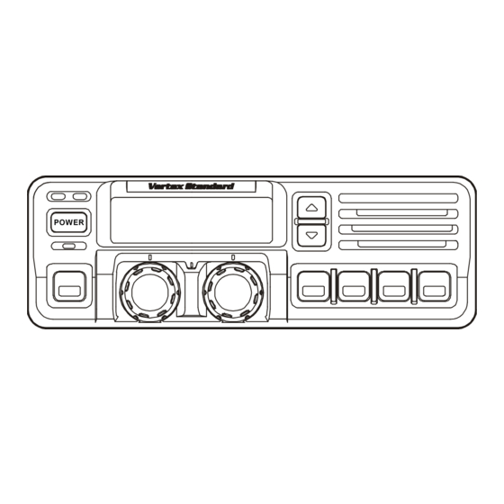
Additional indicators on the display show prior- grammed by your VERTEX STANDARD dealer. ity channel assignments and scan include / ex- clude selection. VOLUME Knob This knob sets the volume of the receiver. - Page 3 Operating Manual Reprint & C ONTROLS ONNECTORS Side Panel Microphone Jack (It is on both sides.) Connect the microphone plug to this jack. Microphone Jack REAR (Heatsink) Antenna Socket 13.4-V DC Power Connector The 50-ohm coaxial feedline to the antenna must The supplied DC power cable must be connected be connected here, using a type-M (PL-259) plug.
- Page 4 Operating Manual Reprint ASIC PERATION OF THE RANSCEIVER Transmitting Important! - Before turning on the radio the first time, confirm that the power connections have been made cor- To transmit, wait until the “BUSY” indicator is rectly and that a proper antenna is connected to the an- off (the channel is not in use), and press the PTT tenna jack.
- Page 5 For further details, contact your VERTEX STAN- by your VERTEX STANDARD dealer, to meet DARD dealer. For future reference, check the box your communications/network requirements. next to each function that has been assigned to...
- Page 6 Operating Manual Reprint DVANCED PERATION Channel Scan ARTS (Auto Range Transpond System) The Scanning feature is used to monitor multiple This system is designed to inform you when you signals programmed into the transceiver. While and another ARTS-equipped station are within scanning, the transceiver will check each channel communication range.
- Page 7 Operating Manual Reprint DVANCED PERATION CH UP/DWN Press the assigned PF button of the “DIM” to ad- Press the assigned PF button of the “CH UP” or just the brightness of the display and key “CH DWN” to select a different channel within backright.
- Page 8 DVANCED PERATION COMP (Compander) Encryption (Option) Press the PF button assigned to the “COMP” When the Voice Scrambler feature is enabled, pressing the assigned PF button of the “Encryp- function to turn the “Compander” IC ON or OFF. This IC contains two variable gain circuits con- tion”...
- Page 9 Operating Manual Reprint PTIONAL CCESSORIES MH-25 Microphone MH-53 Heavy Duty Microphone MH-53 Heavy Duty Microphone w/Noise Canceler MH-53 Heavy Duty DTMF Microphone w/Noise Canceler CE49 Programming Software CT-70 Radio Programming Cable (Requires VPL-1) CT-71 Radio to PC Programming Cable CT-72 Radio to Radio Programming Cable CT-93 CT-81...
- Page 10 Operating Manual Reprint DSUB 25-P CCESSORY ONNECTOR Pin 1: RSSI [Analog Output] A DC voltage proportional to the strength of the signal currently being received (Receiver Signal Strength Indicator) is provided on this pin. This low impedance output is generated by the receiver IF sub-system and buffered by an internal op- amp.
- Page 11 Operating Manual Reprint DSUB 25-P CCESSORY ONNECTOR Similarly, if you assign “CH SW0,” “CH SW1,” 47kΩ DSUB 25-Pin and “CH SW2” to the Universal Input Port, you DSUB 25-Pin can recall Channels 1~7 as shown below: Channel CH SW0 CH SW1 CH SW2 PIN 5 (Pull Up) PINS 2, 3, 4, 6...
- Page 12 Operating Manual Reprint DSUB 25-P CCESSORY ONNECTOR Pin 13: TXDI Pin 17: RX DO [Digital Input for DATA Communications] [Digital Output for DATA Communications] TX Hi-speed Data Input Type (jumper JP2005). RX Hi-speed Data Output Type (jumper Input level 800 mV/600 Ohms, Max.input 1.2V JP2003).
- Page 13 Operating Manual Reprint Note: 1-12...
-
Page 14: Cloning
Cloning includes a convenient “Clone” feature, Now, on the source transceiver, press and hold which allows the programming data from one trans- while turning the transceiver ceiver to be transferred to another . Here is on.Data will now be transferred to the Destina- the procedure for Cloning one radio’s data to anoth- tion transceiver from the source transceiver. -
Page 15: Specifications
Specifications ENERAL Number of Channels: 250 channels Frequency Range: 450 - 480 MHz Channel Spacing: 12.5 / 25 kHz Power Supply Voltage: 13.4V DC ±15 % Current Consumption: Standby: 600 mA Receive: 2.2 A Transmit: 28 A (High) Ambient Temperature Range: –30°C to +60°C (–22°F to +140°F) Frequency Stability: Better than ±2.0 ppm... -
Page 16: Exploded View & Miscellaneous Parts
Exploded View & Miscellaneous Parts ΠRA0332800 Screw List CASE ΠREF. VXSTD P/N Description Qty. ΠU20306007 BINDING HEAD SCREW M3x6B ΠU20306002 BINDING HEAD SCREW M3x6NI ΠU24308002 TAPTITE SCREW M3x8NI ΠU23206001 TAPTITE SCREW M2.6x6 U20305007 BINDING HEAD SCREW M3x5B U32450007 FLAT HEAD SCREW M2.6x5B RA0384100... -
Page 17: Block Diagram
Block Diagram... -
Page 18: Interconnection Diagram
Interconnection Diagram... - Page 19 Interconnection Diagram...
-
Page 20: Circuit Description
Circuit Description Transceiver functions, such as PLL synthesizer PLL Synthesizer settings and channel programming, are controlled The 1st LO, a PLL synthesizer, maintains stabili- via the microprocessor unit (MPU). Reception and ty using a 14.500 MHz reference signal from TCXO transmission are switched by "RX"... - Page 21 Circuit Description Transmitter DCS Demodulator During transmit, the PLL synthesizer oscillates DCS signals are demodulated on the MAIN- at the desired frequency directly, for amplification UNIT, and are applied to low-pass filter Q2110 to obtain RF power output. During transmission, (NJM2902V), as well as the limiter comparator voice modulation and CTCSS (or DCS) modulation Q2003 (NJM2902V).
-
Page 22: Alignment
Alignment Preparation & Precautions Also, VERTEX STANDARD must reserve the right A dummy load and inline wattmeter must be con- to change circuits and alignment procedures in the nected to the main antenna jack in all procedures... - Page 23 Alignment Before beginning, connect the transceiver and PC PLL & Transmitter using the CT-71 programming cable, and download Set up the test equipment as shown for transmit- the EEPROM data from the transceiver to the com- ter alignment. puter. Maintain the supply voltage at 13.4 V DC for all Store this data in a disk file so that it can be saved steps.
- Page 24 Alignment Transmitter Output Power Transmitter Deviation The following transmitter parameters can be ad- The following modulation parameters can be ad- justed from the computer by utilizing the Alignment justed from the computer by utilizing the Alignment Software. Refer to the onboard help of the Align- Software.
- Page 25 Alignment Adjustdjust the AF generator for 50mV (–30dBm) Receiver output at 1 kHz, as applied to the microphone The sensitivity parameters can be adjusted from jack. the computer by utilizing the Alignment Software. Key the transmitter and adjust “MAX Dev ( Nar- Refer to the onboard help of the Alignment Software row ) “...
- Page 26 Squelch Threshold Tight SQL RSSI LEVEL (Narrow) The squelch parameters can also be adjusted from Select the band center frequency channel (CH5), the computer by utilizing the Alignment Software. and with the RF signal generator turned to the Refer to the onboard help of the Alignment Software same frequency, set the generator for ±1.5 kHz Manual for details.
- Page 27 MAIN Unit (Lot. 1-5) Circuit Diagram (0V) (5.62V) (2.15V) (0.21V) 2.2V (5.62V) 13.0V (13.8V) 2.59V (0.97V) (1.09V) 1.37V 6.8V 2.09V 7.45V 0.06V (5.58V) (5.25V) (13.8V) (4.41V) Wide:(0.34V) Narrow:(0.66V) 3.6V (2V) 7.21V (7.18V) (3.57V) 0.56V 2.85V (8.4V) (0.74V) (2.9V) 4.8V (13.5V) (4.5V) (4.98V) (2.45V)
- Page 28 MAIN Unit (Lot. 1-5) Power ON:12.35V (3.93V) (1.18V) Power ON:13.8V OFF:0.3V (1.08V) 4.95V 4.97V 3.9V Power ON:6.85V (8.63V) (2.27V) (8.95V) (3.8V) (3.92V) (2.43V) (4.97V) Power ON:(20 mV) 0.57V OFF:(13.73V) (4.85V) (2.6V) (2.5V) (144mV) (1.93V) (1.94V) (4.97V) (13.2V) (13.77V) (1.95V) (6.1V) (6.15V) (3.92V) (6.19V)
- Page 29 MAIN Unit (Lot. 1-5) Parts Layout M68769H-01 HN58X2432TI (Q1014) (Q2035) MB90F583B (Q2025) NJM2904V TC4W53FU (Q1029) (Q2004) BU4066BF (Q2007) SA7025DK (Q1033) TA31136FN (Q1036) CXA1846N (Q2018) TDA7240AV (Q2019) 2SC2954 (QK) (Q1024:Lot. 1-5) TC4S66F (CQ) MM1216ENRE (1A) (Q2038, 2039) (Q1005) GN2011-Q (4W) (D1023) 2SA1602A (MF) RT1N241M (N2) (Q1023:Lot.
- Page 30 MAIN Unit (Lot. 1-5) NJM2902V 2SB1201STP NJM2904V BU4053BCF 2SJ327Z 2SB1143S MX165CDW (Q2001, 2003, 2108 (Q1006) (Q2042) (Q2016, 2026) (Q2027) (Q1002:Lot. 1-5) (Q2017) 2110) M5223AGP LA8630M (Q1007) (Q2037) IMH6 (H6) IMD3 (D3) TA75S01F (SA) (Q2002) (Q1027) (Q2041) IMX1 (X1) DTB123EK (F12) IMZ1 (Z1) (Q2006) (Q1009, 2021,...
- Page 31 MAIN Unit (Lot. 6-) Circuit Diagram 6A-5...
- Page 32 MAIN Unit (Lot. 6-) 6A-6...
- Page 33 MAIN Unit (Lot. 6-) Parts Layout HN58X2432TI RA45H4452M (Q2035) (Q1014) MB90F583B (Q2025) TC4W53FU (Q2004) BU4066BF (Q2007) SA7025DK (Q1033) TA31136FN (Q1036) CXA1846N (Q2018) TDA7240AV (Q2019) NJM2904V (Q1029) TC4S66F (CQ) MM1216ENRE (1A) (Q2038, 2039) (Q1005) GN2011-Q (4W) SPM5001 RT1N241M (N2) (D1023) (Q1047) (Q1004, 1011, 1017 1039, 2005, 2014 2015, 2040)
- Page 34 MAIN Unit (Lot. 6-) NJM2902V 2SB1201STP NJM2904V TC4W53FU BU4053BCF MX165CDW (Q2001, 2003, 2108 (Q1006) (Q2042) (Q1046) (Q2016, 2026) (Q2017) 2SJ327Z ISA1602AM1 (MF) 2110) M5223AGP 2SC3357-T2 LA8630M (Q2027) (Q2029) (Q1007) (Q1031) (Q2037) IMH6 (H6) IMD3 (D3) TA75S01F (SA) (Q2002) (Q1027) (Q2041) IMX1 (X1) DTB123EK (F12) IMZ1 (Z1)
-
Page 35: Main Unit
MAIN Unit Parts List REF. DESCRIPTION VALUE TOL. MFR’S DESIG VXSTD P/N VERS. LOT. SIDE LAY ADR PCB with Components CB1519001 Printed Circuit Board FR006780C FR006780E C 1001 CHIP CAP. 0.001uF GRM188B11H102KA01D K22174821 C 1002 CHIP CAP. 0.001uF GRM188B11H102KA01D K22174821 C 1003 CHIP CAP. - Page 36 MAIN Unit Parts List REF. DESCRIPTION VALUE TOL. MFR’S DESIG VXSTD P/N VERS. LOT. SIDE LAY ADR C 1049 CHIP CAP. 0.5pF GRM1884C1HR50CZ01D K22174201 C 1051 CHIP CAP. GRM1882C1H4R0CZ01D K22174205 C 1052 CHIP CAP. 0.5pF GRM1884C1HR50CZ01D K22174201 C 1053 CHIP CAP. 470pF GRM1882C1H471JA01D K22174249...
- Page 37 MAIN Unit Parts List REF. DESCRIPTION VALUE TOL. MFR’S DESIG VXSTD P/N VERS. LOT. SIDE LAY ADR C 1101 CHIP CAP. GRM1882C1H6R0CD01D K22174244 C 1101 CHIP CAP. GRM1882C1H7R0CZ01D K22174245 C 1102 CHIP CAP. GRM1882C1H5R0CZ01D K22174206 C 1104 CHIP CAP. 0.1uF GRM188B11C104KA01D K22124805 C 1105 CHIP CAP.
- Page 38 MAIN Unit Parts List REF. DESCRIPTION VALUE TOL. MFR’S DESIG VXSTD P/N VERS. LOT. SIDE LAY ADR C 1153 CHIP CAP. GRM1882C1H9R0DZ01D K22174210 C 1154 CHIP CAP. GRM1882C1H6R0DZ01D K22174207 C 1155 CHIP CAP. GRM1882C1H4R0CZ01D K22174205 C 1156 CHIP CAP. GRM1882C1H8R0DZ01D K22174209 C 1157 CHIP CAP.
- Page 39 MAIN Unit Parts List REF. DESCRIPTION VALUE TOL. MFR’S DESIG VXSTD P/N VERS. LOT. SIDE LAY ADR C 1208 CHIP CAP. 100pF GRM1882C1H101JA01D K22174235 C 1209 CHIP CAP. 10pF GRM1882C1H100JA01D K22174211 C 1210 CHIP CAP. 33pF GRM1882C1H330JA01D K22174223 C 1211 CHIP CAP. 0.001uF GRM188B11H102KA01D K22174821...
- Page 40 MAIN Unit Parts List REF. DESCRIPTION VALUE TOL. MFR’S DESIG VXSTD P/N VERS. LOT. SIDE LAY ADR C 1260 CHIP CAP. 0.01uF ECJ1VB1H103K K22179626 C 1260 CHIP CAP. 0.01uF GRM188B11H103KA01D K22174823 C 1261 CHIP TA.CAP. 10uF 6.3V TEESVA0J106M8R K78080027 C 1262 CHIP CAP. 220pF GRM1882C1H221JA01D K22174243...
- Page 41 MAIN Unit Parts List REF. DESCRIPTION VALUE TOL. MFR’S DESIG VXSTD P/N VERS. LOT. SIDE LAY ADR C 2005 CHIP CAP. 100pF GRM1882C1H101JA01D K22174235 C 2006 CHIP CAP. 100pF GRM1882C1H101JA01D K22174235 C 2007 CHIP CAP. 100pF GRM1882C1H101JA01D K22174235 C 2008 CHIP CAP. 100pF GRM1882C1H101JA01D K22174235...
- Page 42 MAIN Unit Parts List REF. DESCRIPTION VALUE TOL. MFR’S DESIG VXSTD P/N VERS. LOT. SIDE LAY ADR C 2065 CHIP CAP. 0.022uF GRM188B11H223KA01D K22174839 C 2066 CHIP CAP. 0.1uF GRM188B11C104KA01D K22124805 C 2067 CHIP CAP. 0.1uF GRM188B11C104KA01D K22124805 C 2068 CHIP CAP. 0.1uF GRM188B11C104KA01D K22124805...
- Page 43 MAIN Unit Parts List REF. DESCRIPTION VALUE TOL. MFR’S DESIG VXSTD P/N VERS. LOT. SIDE LAY ADR C 2118 CHIP CAP. 0.0015uF GRM188B11H152KA01D K22174827 C 2119 CHIP CAP. 0.1uF GRM188B11C104KA01D K22124805 C 2120 CHIP CAP. 0.001uF GRM188B11H102KA01D K22174821 C 2121 CHIP TA.CAP. 4.7uF TEESVA1C475M8R K78120031...
- Page 44 MAIN Unit Parts List REF. DESCRIPTION VALUE TOL. MFR’S DESIG VXSTD P/N VERS. LOT. SIDE LAY ADR C 2162 CHIP TA.CAP. 10uF TEESVA1A106M8R K78100028 C 2163 CHIP CAP. 0.01uF ECJ1VB1H103K K22179626 C 2163 CHIP CAP. 0.01uF GRM188B11H103KA01D K22174823 C 2164 CHIP CAP. 0.047uF GRM39B473K16PT K22124804...
- Page 45 MAIN Unit Parts List REF. DESCRIPTION VALUE TOL. MFR’S DESIG VXSTD P/N VERS. LOT. SIDE LAY ADR D 1019 DIODE BAS316 G2070716 D 1021 DIODE HZM5.6NB2 TR-E G2070722 D 1022 DIODE 1SS321(TE85R.F) G2070076 D 1023 IC GN2011-Q(TX) G1092183 D 1024 DIODE MC2848-T111-1 G2070694 D 1026 DIODE...
- Page 46 MAIN Unit Parts List REF. DESCRIPTION VALUE TOL. MFR’S DESIG VXSTD P/N VERS. LOT. SIDE LAY ADR L 1019 COIL E2 0.4-1.5-4T-L L0022475 L 1020 COIL E2 0.35-1.6-4T-L L0022456 L 1021 COIL E2 0.35-1.6-4T-L L0022456 L 1022 CHIP COIL 0.0147uH LQW31HN15NJ03L L1690251 L 1023 M.RFC...
- Page 47 Q 2032 TRANSISTOR RT1N241M-T11-1 G3070249 Q 2034 IC RN5VL35AA-TR G1091666 Q 2035 IC HN58X2432TI G1093315 Q 2036 TRANSISTOR RT1N241M-T11-1 G3070249 Q 2037 IC LA8630M-B-TLM-E G1093452 Q 2038 IC TC4S66F(TE85R.F) G1090893 Q 2039 IC TC4S66F(TE85R.F) G1090893 : Please contact VERTEX STANDARD. 6A-21...
- Page 48 MAIN Unit Parts List REF. DESCRIPTION VALUE TOL. MFR’S DESIG VXSTD P/N VERS. LOT. SIDE LAY ADR Q 2040 TRANSISTOR RT1N241M-T11-1 G3070249 Q 2041 IC TA75S01F(TE85R.F) G1091593 Q 2042 IC NJM2904V-TE1 G1091677 Q 2108 IC NJM2902V-TE1 G1091679 Q 2110 IC NJM2902V-TE1 G1091679 R 1001 CHIP RES.
- Page 49 MAIN Unit Parts List REF. DESCRIPTION VALUE TOL. MFR’S DESIG VXSTD P/N VERS. LOT. SIDE LAY ADR R 1049 CHIP RES. 330k 1/16W 5% RMC1/16 334JATP J24185334 R 1050 CHIP RES. 1/16W 5% RMC1/16 103JATP J24185103 R 1051 CHIP RES. 1.2k 1/16W 5% RMC1/16 122JATP...
- Page 50 MAIN Unit Parts List REF. DESCRIPTION VALUE TOL. MFR’S DESIG VXSTD P/N VERS. LOT. SIDE LAY ADR R 1092 CHIP RES. 1/16W 5% RMC1/16 000JATP J24185000 R 1093 CHIP RES. 1/10W 5% RMC1/10T 330J J24205330 R 1094 CHIP RES. 1/10W 5% RMC1/10T 220J J24205220 R 1095 CHIP RES.
- Page 51 MAIN Unit Parts List REF. DESCRIPTION VALUE TOL. MFR’S DESIG VXSTD P/N VERS. LOT. SIDE LAY ADR R 1143 CHIP RES. 1/16W 5% RMC1/16 123JATP J24185123 R 1145 CHIP RES. 150k 1/16W 5% RMC1/16 154JATP J24185154 R 1146 CHIP RES. 2.2k 1/16W 5% RMC1/16 222JATP...
- Page 52 MAIN Unit Parts List REF. DESCRIPTION VALUE TOL. MFR’S DESIG VXSTD P/N VERS. LOT. SIDE LAY ADR R 1201 CHIP RES. 3.3k 1/16W 5% RMC1/16 332JATP J24185332 R 1202 CHIP RES. 1/16W 5% RMC1/16 103JATP J24185103 R 1203 CHIP RES. 1/16W 5% RMC1/16 103JATP J24185103...
- Page 53 MAIN Unit Parts List REF. DESCRIPTION VALUE TOL. MFR’S DESIG VXSTD P/N VERS. LOT. SIDE LAY ADR R 2054 CHIP RES. 4.7k 1/16W 5% RMC1/16 472JATP J24185472 R 2055 CHIP RES. 100k 1/16W 5% RMC1/16 104JATP J24185104 R 2056 CHIP RES. 1/16W 5% RMC1/16 473JATP J24185473...
- Page 54 MAIN Unit Parts List REF. DESCRIPTION VALUE TOL. MFR’S DESIG VXSTD P/N VERS. LOT. SIDE LAY ADR R 2112 CHIP RES. 1/16W 5% RMC1/16 273JATP J24185273 R 2112 CHIP RES. 1/16W 5% RMC1/16 563JATP J24185563 R 2113 CHIP RES. 1/16W 5% RMC1/16 103JATP J24185103 R 2114 CHIP RES.
- Page 55 MAIN Unit Parts List REF. DESCRIPTION VALUE TOL. MFR’S DESIG VXSTD P/N VERS. LOT. SIDE LAY ADR R 2170 CHIP RES. 1/16W 5% RMC1/16 105JATP J24185105 R 2171 CHIP RES. 330k 1/16W 5% RMC1/16 334JATP J24185334 R 2172 CHIP RES. 5.6k 1/16W 5% RMC1/16 562JATP...
- Page 56 MAIN Unit Parts List REF. DESCRIPTION VALUE TOL. MFR’S DESIG VXSTD P/N VERS. LOT. SIDE LAY ADR R 2229 CHIP RES. 1/16W 5% RMC1/16 473JATP J24185473 R 2229 CHIP RES. 100k 1/16W 5% RMC1/16 104JATP J24185104 R 2230 CHIP RES. 1/16W 5% RMC1/16 473JATP J24185473...
- Page 57 DISPLAY Unit (Lot. 1-5) Circuit Diagram 6B-1...
- Page 58 DISPLAY Unit (Lot. 1-5) Note: 6B-2...
- Page 59 DISPLAY Unit (Lot. 1-5) Parts Layout Side A S-93C46AMFN-TB 2SB1132Q (BA) RT1N241M (N2) (Lot. 1-3) NJM78L05UA (8C) MC2848 (A6) DAP202U (P) MC2850 (A7) (Q3012) (Q3031) (Q3003) (Q3021) (D3008) (D3006) (D3018, 3019) DTC323TK (H02) (Lot. 4-) (Q3003) 6B-3...
- Page 60 DISPLAY Unit (Lot. 1-5) Parts Layout Side B NJM2902V (Q3039) RN5VL35AA (C5) (Lot. 1-5) IMD3 (D3) IMZ1 (Z1) 2SC4154E (LE) RT1N241M (N2) PDTC114TE (24) (Lot. 1-3) 1SS226 (C3) HD64F3642AH (Q3016) (Q3013) (Q3004, 3011, 3040) (Q3019) (Q3005, 3020, 3022, (Q3009) (D3005) (Q3014) IMX1 (X1) 3024, 3025, 3026,...
- Page 61 DISPLAY Unit (Lot. 6-) Circuit Diagram 6B-5...
- Page 62 DISPLAY Unit (Lot. 6-) Note: 6B-6...
- Page 63 DISPLAY Unit (Lot. 6-) Parts Layout Side A S-93C46AMFN-TB 2SB1132Q (BA) NJM78L05UA (8C) MC2848 (A6) DAP202U (P) MC2850 (A7) (Q3012) (Q3031) (Q3021) (D3008) (D3006) (D3018, 3019) 6B-7...
- Page 64 DISPLAY Unit (Lot. 6-) Parts Layout Side B NJM2060V (Q3039) IMD3 (D3) IMZ1 (Z1) 2SC4154E (LE) RT1N241M (N2) DTC323TK (H02) S-80835CNMC 1SS226 (C3) HD64F3642AH (Q3013) (Q3004, 3011, 3040) (Q3019) (Q3005, 3020, 3022, (Q3008, 3009) (Q3016) (D3005) (Q3014) IMX1 (X1) 3024, 3025, 3026, (Q3010, 3038) 3027) 2SB1132Q (BA)
-
Page 65: Display Unit
DISPLAY Unit Parts List REF. DESCRIPTION VALUE TOL. MFR’S DESIG VXSTD P/N VERS. LOT. SIDE LAY ADR PCB with Components CB1670001 Printed Circuit Board FR004690D FR004690E C 3001 CHIP CAP. 0.1uF GRM188B11C104KA01D K22124805 C 3002 CHIP CAP. 0.1uF GRM188B11C104KA01D K22124805 C 3003 CHIP CAP. - Page 66 DISPLAY Unit Parts List REF. DESCRIPTION VALUE TOL. MFR’S DESIG VXSTD P/N VERS. LOT. SIDE LAY ADR C 3049 CHIP CAP. 33pF GRM1882C1H330JA01D K22174223 C 3050 CHIP CAP. 0.01uF GRM188B11H103KA01D K22174823 C 3051 CHIP CAP. 0.1uF GRM188B11C104KA01D K22124805 C 3053 AL.ELECTRO.CAP. 100uF EEE1CA101WP K48120012...
- Page 67 DISPLAY Unit Parts List REF. DESCRIPTION VALUE TOL. MFR’S DESIG VXSTD P/N VERS. LOT. SIDE LAY ADR Q 3001 IC LC75823W-E G1092941 Q 3003 TRANSISTOR RT1N241M-T11-1 G3070249 Q 3003 TRANSISTOR DTC323TK T146 G3070042 Q 3004 TRANSISTOR IMZ1 T108 G3070025 Q 3005 TRANSISTOR RT1N241M-T11-1 G3070249 Q 3008 TRANSISTOR...
- Page 68 DISPLAY Unit Parts List REF. DESCRIPTION VALUE TOL. MFR’S DESIG VXSTD P/N VERS. LOT. SIDE LAY ADR R 3031 CHIP RES. 1/16W 5% RMC1/16 223JATP J24185223 R 3031 CHIP RES. 1/16W 5% RMC1/16 000JATP J24185000 R 3033 CHIP RES. 1.5M 1/16W 5% RMC1/16 155JATP J24185155...
- Page 69 DISPLAY Unit Parts List REF. DESCRIPTION VALUE TOL. MFR’S DESIG VXSTD P/N VERS. LOT. SIDE LAY ADR R 3078 CHIP RES. 1/16W 5% RMC1/16 473JATP J24185473 R 3079 CHIP RES. 1/16W 5% RMC1/16 153JATP J24185153 R 3080 CHIP RES. 220k 1/16W 5% RMC1/16 224JATP J24185224...
- Page 70 DISPLAY Unit Parts List REF. DESCRIPTION VALUE TOL. MFR’S DESIG VXSTD P/N VERS. LOT. SIDE LAY ADR R 3146 CHIP RES. 1/4W RMC1/4 221JATP J24245221 R 3147 CHIP RES. 1/16W 5% RMC1/16 000JATP J24185000 R 3150 CHIP RES. 1/4W RMC1/4 471JATP J24245471 R 3152 CHIP RES.
- Page 71 KEY Unit Circuit Diagram 1.96V 3.9V 5.8V 1.92V 3.82V 4.62V 7.71V 4.95V 4.53V 4.61V 3.18V 3.87V 4.19V 4.34V 4.46V 2SA1602A (MF) (Lot. 1-6) ISA1602AM1 (MF) (Lot. 7-) (Q3401) (Q3401) Parts Layout Side A Side B 6C-1...
- Page 72 KEY Unit Note: 6C-2...
-
Page 73: Key Unit
KEY Unit Parts List REF. DESCRIPTION VALUE TOL. MFR’S DESIG VXSTD P/N VERS. LOT. SIDE LAY ADR PCB with Components CB1671001 Printed Circuit Board FR006070D C 3402 CHIP CAP. 0.001uF GRM188B11H102KA01D K22174821 D 3401 LED TLOU1008(T04) G2070796 D 3402 LED TLOU1008(T04) G2070796 D 3403 LED... - Page 74 KEY Unit Note:...
-
Page 75: Vr Unit
VR Unit Circuit Diagram (Lot. 1-5) Parts Layout (Lot. 1-5) J3601 S3601 VR3601 Side A R3606 C3603 R3602 R3603 R3607 R3605 C3604 C3606 Side B Circuit Diagram (Lot. 6-) Parts Layout (Lot. 6-) Side A Side B... - Page 76 VR Unit Parts List REF. DESCRIPTION VALUE TOL. MFR’S DESIG VXSTD P/N VERS. LOT. SIDE LAY ADR PCB with Components CB1672001 Printed Circuit Board FR006080C FR006080D C 3601 CHIP CAP. 0.01uF GRM39B103K25PT K22144803 C 3602 CHIP CAP. 0.01uF GRM39B103K25PT K22144803 C 3603 CHIP CAP.
-
Page 77: Mic Conn Unit
MIC CONN Unit (Lot. 1-6) Circuit Diagram Parts Layout Side A Side B Parts List REF. DESCRIPTION VALUE TOL. MFR’S DESIG VXSTD P/N VERS. LOT. SIDE LAY ADR PCB with Components Printed Circuit Board FR006090C J 3901 CONNECTOR 14FE-ST-VK-N P1091103 J 3902 CONNECTOR BM14B-SRSS-TBT... -
Page 78: Mic Conn-2 Unit
MIC CONN-2 Unit (Lot. 6-) Circuit Diagram Parts Layout Side A Side B Parts List REF. DESCRIPTION VALUE TOL. MFR’S DESIG VXSTD P/N VERS. LOT. SIDE LAY ADR PCB with Components CB4296001 Printed Circuit Board FR017700A C 3956 CHIP CAP. 0.01uF GRM155B11E103KA01D K22148834... - Page 79 PA Unit (Lot. 1-8) Circuit Diagram Parts Layout 13.8V (12.9V) 18.9V (0V) 0.4V (0V) 1.4V (0.2V) Side A XX : TX 465.01 MHz, High Power, 50-ohm (XX) : RX 2SC3102 HSM88AS C30T04Q (Q6001, 6002) (C1) (D6004) (D6002, 6003) Side B 6G-1...
- Page 80 PA Unit (Lot. 9-) Circuit Diagram Parts Layout 13.8V (12.9V) 18.9V (0V) 0.4V (0V) 1.4V (0.2V) Side A RD60HUF1 HSM88AS C30T04Q (Q6001, 6002) (C1) (D6004) (D6002, 6003) Side B 6G-2...
-
Page 81: Pa Unit
PA Unit Parts List REF. DESCRIPTION VALUE TOL. MFR’S DESIG VXSTD P/N VERS. LOT. SIDE LAY ADR PCB with Components CS2085101 Printed Circuit Board FR006790C FR006790E C 6002 FILM CAP. 100pF 500V UC232H1000J-T K33279048 C 6003 FILM CAP. 100pF 500V UC232H1000J-T K33279048 C 6008 FILM CAP. - Page 82 PA Unit Parts List REF. DESCRIPTION VALUE TOL. MFR’S DESIG VXSTD P/N VERS. LOT. SIDE LAY ADR C 6045 FILM CAP. 500V UC232H0040D-T K33279044 C 6045 CHIP CAP. 500V CF316CH4R0C500AT K22271249 C 6046 FILM CAP. 500V UC232H0050D-T K33279010 C 6046 FILM CAP. 500V UC232H0040D-T K33279044...
- Page 83 PA Unit Parts List REF. DESCRIPTION VALUE TOL. MFR’S DESIG VXSTD P/N VERS. LOT. SIDE LAY ADR R 6015 CHIP RES. 1/16W 5% RMC1/16 223JATP J24185223 R 6016 CHIP RES. 1/16W 5% RMC1/16 102JATP J24185102 R 6017 CHIP RES. 1/16W 5% RMC1/16 000JATP J24185000 R 6018 CHIP RES.
- Page 84 PA Unit Note...
-
Page 85: F2D-8 2-Tone Decode Unit
F2D-8 2-Tone Decode Unit Circuit Diagram Parts Layout Side A Side B TC7S04FU (E5) TA75S01F (SA) DTC124TU (05) HD64F3334YTF16 (Q1003) (Q1004) (Q1005) (Q1001) 7A-1... - Page 86 F2D-8 2-Tone Decode Unit Parts List REF. DESCRIPTION VALUE TOL. MFR’S DESIG VXSTD P/N VERS. LOT. SIDE LAY ADR *** F2D-8 *** Printed Circuit Board FR002530C C 1001 CHIP TA.CAP. 4.7uF 6.3V TEMSVA0J475M-8R K78080017 C 1002 CHIP CAP. 0.001uF GRM39B102K50PT K22174821 C 1003 CHIP CAP.
-
Page 87: Vtp-50 Vx-Trunk Unit
VTP-50 VX-Trunk Unit Circuit Diagram Parts Layout Side B Side A BR93LC56FV NJM2904V MC68HSC705C8A502 TA75S01F (SA) (Q1004) (Q1001) (Q1002) (Q1003) 7B-1... - Page 88 VTP-50 VX-Trunk Unit Parts List REF. DESCRIPTION VALUE TOL. MFR’S DESIG VXSTD P/N VERS. LOT. SIDE LAY ADR *** VTP-50 *** Printed Circuit Board FR002540C C 1002 CHIP CAP. 0.001uF GRM39B102K50PT K22174821 C 1003 CHIP CAP. 0.01uF GRM39B103M25PT K22144802 C 1003 CHIP CAP. 0.01uF GRM39B103K25PT K22144803...
-
Page 89: Fvp-25 Encryption / Dtmf Pager Unit
FVP-25 Encryption / DTMF Pager Unit Circuit Diagram Parts Layout Side A Side B M64026FP LC73881 DTC144EU (26) (Q1001) (Q1002) (Q1003) 7C-1... - Page 90 FVP-25 Encryption / DTMF Pager Unit Parts List REF. DESCRIPTION VALUE TOL. MFR’S DESIG VXSTD P/N VERS. LOT. SIDE LAY ADR *** FVP-25 *** Printed Circuit Board FR005010F C 1001 CHIP CAP. 0.1uF GRM39B104K16PT K22124805 C 1002 CHIP CAP. 0.01uF GRM39B103M25PT K22144802 C 1003 CHIP CAP.
-
Page 91: F5D-14 5-Tone Unit
F5D-14 5-Tone Unit Circuit Diagram Parts Layout Side A Side B TK71650SC (L50) DTC114TE (04) PIC17LC44-08/PQ 2SC4617 (BR) MD09 BR93LC66FV (Q1001) (Q1002) (Q1003) (Q1004) (Q1005) (Q1006) 7D-1... - Page 92 F5D-14 5-Tone Unit Parts List REF. DESCRIPTION VALUE TOL. MFR’S DESIG VXSTD P/N VERS. LOT. SIDE LAY ADR *** F5D-14 *** Printed Circuit Board FR006510B Printed Circuit Board FR006510D C 1001 CHIP CAP. 0.1uF GRM36B104K10PT K22108802 C 1002 CHIP CAP. 0.0018uF GRM36B182K50PT K22178812...
-
Page 93: Fif-7A Connection Unit
FIF-7A Connection Unit Circuit Diagram Parts Layout Side A Side B TC7WT125FU NJM2902V (Q1008, 1011, TK71635SCL (L35) TC7S04FU (E5) (Q1001) 1012) (Q1003) (Q1004) 7E-1... - Page 94 FIF-7A Connection Unit Parts List REF. DESCRIPTION VALUE TOL. MFR’S DESIG VXSTD P/N VERS. LOT. SIDE LAY ADR *** FIF-7A *** Printed Circuit Board FR007860A Printed Circuit Board FR007860B C 1001 CHIP CAP. 0.1uF GRM39B104K16PT K22124805 C 1002 CHIP CAP. 68pF GRM39CH680J50PT K22174231...
- Page 95 FIF-7A Connection Unit REF. DESCRIPTION VALUE TOL. MFR’S DESIG VXSTD P/N VERS. LOT. SIDE R 1007 CHIP RES. 1/16W RMC1/16 000JATP J24185000 R 1008 CHIP RES. 1/16W RMC1/16 103JATP J24185103 R 1009 CHIP RES. 150k 1/16W RMC1/16 154JATP J24185154 R 1011 CHIP RES. 1/16W RMC1/16 000JATP J24185000...
- Page 96 FIF-7A Connection Unit Note: 7E-4...
- Page 97 No portion of this manual © Copyright 2011 may be reproduced VERTEX STANDARD CO., LTD. without the ermission of All rights reserved VERTEX STANDARD CO., LTD.
Need help?
Do you have a question about the VX-6000U and is the answer not in the manual?
Questions and answers