
Related Manuals for Asus AAEON BOXER-8645AI


Summary of Contents for Asus AAEON BOXER-8645AI
- Page 1 BOXER-8645AI AI@Edge Fanless Embedded AI System with NVIDIA® Jetson AGX Orin™ User’s Manual 1 Last Updated: March 11, 2024...
- Page 2 Copyright Notice This document is copyrighted, 2024. All rights are reserved. The original manufacturer reserves the right to make improvements to the products described in this manual at any time without notice. No part of this manual may be reproduced, copied, translated, or transmitted in any form or by any means without the prior written permission of the original manufacturer.
- Page 3 Acknowledgements All other products’ name or trademarks are properties of their respective owners. NVIDIA®, the NVIDIA logo, Jetson™, Jetson Orin™, and JetPack™ are ⚫ trademarks of the NVIDIA Corporation. Arm® and Arm®v8-M architecture are registered trademarks of Arm Limited. ⚫ Linux®...
- Page 4 Packing List Before setting up your product, please make sure the following items have been shipped: Item Quantity BOXER-8645AI ⚫ HDMI Cable Holder ⚫ Screw Package ⚫ Power Connector ⚫ Power Adapter (Optional) ⚫ Power Cord (Optional) ⚫ If any of these items are missing or damaged, please contact your distributor or sales representative immediately.
- Page 5 About this Document This User’s Manual contains all the essential information, such as detailed descriptions and explanations on the product’s hardware and software features (if any), its specifications, dimensions, jumper/connector settings/definitions, and driver installation instructions (if any), to facilitate users in setting up their product. Users may refer to the product page at AAEON.com for the latest version of this document.
- Page 6 Safety Precautions Please read the following safety instructions carefully. It is advised that you keep this manual for future references All cautions and warnings on the device should be noted. All cables and adapters supplied by AAEON are certified and in accordance with the material safety laws and regulations of the country of sale.
- Page 7 As most electronic components are sensitive to static electrical charge, be sure to ground yourself to prevent static charge when installing the internal components. Use a grounding wrist strap and contain all electronic components in any static-shielded containers. If any of the following situations arises, please the contact our service personnel: Damaged power cord or plug Liquid intrusion to the device iii.
- Page 8 FCC Statement This device complies with Part 15 FCC Rules. Operation is subject to the following two conditions: (1) this device may not cause harmful interference, and (2) this device must accept any interference received including interference that may cause undesired operation.
- Page 9 China RoHS Requirements (CN) 产品中有毒有害物质或元素名称及含量 AAEON System QO4-381 Rev.A0 有毒有害物质或元素 部件名称 铅 汞 镉 六价铬 多溴联苯 多溴二苯 醚(PBDE) (Pb) (Hg) (Cd) (Cr(VI)) (PBB) 印刷电路板 × ○ ○ ○ ○ ○ 及其电子组件 外部信号 × ○ ○ ○ ○ ○ 连接器及线材 外壳 ○...
- Page 10 China RoHS Requirement (EN) Hazardous and Toxic Materials List AAEON System QO4-381 Rev.A0 Hazardous or Toxic Materials or Elements Component Name PCB and Components Wires & Connectors for Ext.Connections Chassis CPU & RAM HDD Drive LCD Module Optical Drive Touch Control Module Battery This form is prepared in compliance with the provisions of SJ/T 11364.
-
Page 11: Table Of Contents
Table of Contents Chapter 1 - Product Specifications..................1 Specifications ......................2 Chapter 2 – Hardware Information ..................5 Dimensions ....................... 6 Jumpers and Connectors ..................9 List of Jumpers ......................11 2.3.1 Jumper Settings ..................11 2.3.2 Automation Header (CN28) ..............12 2.3.3 MCU Control Delay ON/OFF Setting (JP3) ........ - Page 12 2.4.16 UART Debug Wafer Box (CN18) ............33 2.4.17 SATA 1/2 (CN20/CN21) ................. 34 2.4.18 5V SATA Power Connector 1/2 (CN22/CN23) ......... 34 2.4.19 CANBus FD Isolated Connector (CN24) ........... 35 2.4.20 8-bit DIO Connector (CN25)............... 35 2.4.21 GPS & IMU Sensor Board (CN26) ............36 2.4.22 Reserve Connector (CN29) ..............
- Page 13 Flash Image to Board .................... 77 Check BSP Version ....................78 Chapter 4 – OS User Guide ....................79 Introduction ......................80 Update Note ......................81 Power Mode for BOXER-8645AI ................ 82 DIO/GPIO Setting Command ................83 GNSS Sensor......................85 IMU Sensor ......................
-
Page 14: Chapter 1 - Product Specifications
Chapter 1 Chapter 1 - Product Specifications... -
Page 15: Specifications
Specifications System AI Accelerator NVIDIA® Jetson AGX Orin™ AGX Orin 32GB: 8-core Arm® Cortex®-A78AE CPU AGX Orin 64GB: 12-core Arm® Cortex®-A78AE CPU System Memory 32GB LPDDR5 64GB LPDDR5 Storage Device 64GB eMMC 5.1 M.2 2280 M-Key x 1 (NVMe) 2.5” SATA x 2 Display Interface HDMI 2.0 (Type-A) x 1 Ethernet... - Page 16 System GNSS Support 9-Axis Sensor Support Expansion M.2 2230 E-Key x 1 (Wi-Fi/BT) M.2 3052 B-Key x 1 (LTE) M.2 2280 M-Key x 1 (NVMe) 2.5” SATA x 2 SIM Slot x 2 MicroSD Slot x 1 Indicator Power LED x 1 OS Support Linux (NVIDIA JetPack™...
- Page 17 Environmental Anti-Vibration MIL-STD-810G, 514.6C Procedure 1, Category 4 Trucker/Semitrailer on US highway (Figure 514.6C-1-Category 4-Common carrier) Anti-Shock MIL-STD-810G, Method 516.6, Procedure I, flight vehicle equipment Certification E-Mark, CE/FCC Class A Note: The real USB, LAN and COM transmission rate depends on the user scenario and HW design.
-
Page 18: Chapter 2 - Hardware Information
Chapter 2 Chapter 2 – Hardware Information... -
Page 19: Dimensions
Dimensions System Chapter 2 – Hardware Information... - Page 20 Non-standard Version Dimension (Additional RJ-45 x 8) Note: Available upon request with MOQ. Chapter 2 – Hardware Information...
- Page 21 Non-standard Version Dimension (Additional M12 x 8) Note: Available upon request with MOQ. Chapter 2 – Hardware Information...
-
Page 22: Jumpers And Connectors
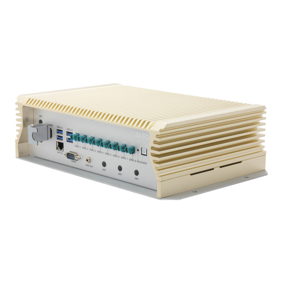
Jumpers and Connectors Component Side Chapter 2 – Hardware Information... - Page 23 Solder Side Chapter 2 – Hardware Information...
-
Page 24: List Of Jumpers
List of Jumpers The board has a number of jumpers that allow you to configure your system to suit your application. The table below shows the function of each of the board's jumpers Label Function CN28 Automation Header MCU Control Delay ON/OFF Setting 2.3.1 Jumper Settings You configure your card to match the needs of your application by setting jumpers. -
Page 25: Automation Header (Cn28)
2.3.2 Automation Header (CN28) Function FORCE_RECOVERY SYS_RST BUTTON_POWER SHORT: AUTO POWER ON ENABLE OPEN: AUTO POWER ON DISABLE CVB_STBY(SLEEP) SYSTEM_OC_N 9-10 OPEN: WOL DISABLE 9-10 SHORT: WOL ENABLE 11-12 Scandump 3V3_AO 5V_AO Chapter 2 – Hardware Information... -
Page 26: Mcu Control Delay On/Off Setting (Jp3)
2.3.3 MCU Control Delay ON/OFF Setting (JP3) Chapter 2 – Hardware Information... -
Page 27: The Chassis Mark (Sw1/Sw2)
2.3.4 The Chassis Mark (SW1/SW2) Chapter 2 – Hardware Information... -
Page 28: List Of Connectors
List of Connectors The board has a number of connectors that allow you to configure your system to suit your application. The table below shows the function of each of the board's connectors Label Function NVIDIA Jetson AGX Orin Module Connector RTC Battery Connector HDMI Port GbE LAN + Dual USB 3.2 Ports... - Page 29 Label Function CN31 M.2 3052 B-Key Slot CN32/CN38 SIM Slot CN33 M.2 2230 E-Key Slot CN34 M.2 2280 M-Key Slot CN35 Phoenix Connector Power Button Recovery Button Reset Button J1~J8 GMSL2 Camera FAKRA Connector CN39 NCSI Header for OOB Module Chapter 2 –...
-
Page 30: Nvidia Jetson Agx Orin Module Connector (Cn1)
2.4.1 NVIDIA Jetson AGX Orin Module Connector (CN1) Chapter 2 – Hardware Information... - Page 31 Chapter 2 – Hardware Information...
- Page 32 Chapter 2 – Hardware Information...
-
Page 33: Rtc Battery Connector (Cn2)
2.4.2 RTC Battery Connector (CN2) Pin Name Signal Type Signal Level +V3P3A_RTC +3.3V 2.4.3 HDMI Port (CN4) Pin Name Signal Type Signal Level HDMI_TXD2_CON_P DIFF HDMI_TXD2_CON_N DIFF HDMI_TXD1_CON_P DIFF HDMI_TXD1_CON_N DIFF HDMI_TXD0_CON_P Chapter 2 – Hardware Information... -
Page 34: Gbe Lan + Dual Usb 3.2 Ports (Cn5)
Pin Name Signal Type Signal Level HDMI_TXD0_CON_N HDMI_TXC_CON_P DIFF HDMI_TXC_CON_N DIFF HDMI_CEC_CON 3.3V HDMI_DDC_SCL_5V0 HDMI_DDC_SDA_5V0 VDD_5V0_HDMI_CON HDMI_HPD_CON 2.4.4 GbE LAN + Dual USB 3.2 Ports (CN5) Pin Name Signal Type Signal Level LAN1_MDI0+ DIFF LAN1_MDI0- DIFF LAN1_MDI1+ DIFF LAN1_MDI1- DIFF Chapter 2 –... - Page 35 Pin Name Signal Type Signal Level LAN1_MDI2+ DIFF LAN1_MDI2- DIFF LAN1_MDI3+ DIFF LAN1_MDI3- DIFF VCC_USB3 USB3- DIFF USB3+ DIFF USB3_RX3_N_C DIFF USB3_RX3_P_C DIFF USB3_TX3_N_C DIFF USB3_TX3_P_C DIFF VCC_USB4 USB4- DIFF USB4+ DIFF USB3_RX4_N_C DIFF USB3_RX4_P_C DIFF USB3_TX4_N_C DIFF USB3_TX4_P_C DIFF Link/Speed Active LAN speed...
-
Page 36: Lan Port (Cn6)
2.4.5 10G LAN Port (CN6) Pin Name Signal Type Signal Level MGBE1_PHY_A_N_CN DIFF MGBE1_PHY_A_P_CN DIFF MGBE1_PHY_B_P_CN DIFF MGBE1_PHY_B_N_CN DIFF MGBE1_PHY_C_P_CN DIFF MGBE1_PHY_C_N_CN DIFF MGBE1_PHY_D_N_CN DIFF MGBE1_PHY_D_P_CN DIFF Chapter 2 – Hardware Information... -
Page 37: Pcie [X8] Slot (Cn7)
2.4.6 PCIe [x8] Slot (CN7) Signal Signal Signal Signal Pin Name Pin Name Type Level Type Level +12V +12V +12V +12V +12V +12V +12V +12V +12V +12V I2C_GP3_CLK_PEX_3V3 +3.3V I2C_GP3_DAT_PEX_3V3 IN/OUT +3.3V VDD_3V3 +3.3V VDD_3V3 +3.3V VDD_3V3 +3.3V 3V3_AO +3.3V PCIE5_RST_N_CON IN +3.3V PEX_WAKE_N_CON... - Page 38 Signal Signal Signal Signal Pin Name Pin Name Type Level Type Level UPHY1_TX1_N_C DIFF UPHY1_RX1_P DIFF UPHY1_RX1_N DIFF UPHY1_TX2_P_C DIFF UPHY1_TX2_N_C DIFF UPHY1_RX2_P DIFF UPHY1_RX2_N DIFF UPHY1_TX3_P_C DIFF UPHY1_TX3_N_C DIFF UPHY1_RX3_P DIFF UPHY1_RX3_N DIFF PCIE_PRSNT_CON_L +3.3V IO_PWR_EN +3.3V UPHY1_TX4_P_C DIFF UPHY1_TX4_N_C DIFF UPHY1_RX4_P...
-
Page 39: Audio Header (Cn10)
Signal Signal Signal Signal Pin Name Pin Name Type Level Type Level UPHY1_RX7_N DIFF PCIE_PRSNT_CON_L +3.3V 2.4.7 Audio Header (CN10) Signal Signal Signal Signal Pin Name Pin Name Type level Type level IN1P IN2P AUD_GPIO4 IN/OUT AUD_HPOR AUD_MIC_JD SENSE_SEND GND AUD_HPOL AUD_HP_JD Chapter 2 –... -
Page 40: Dual Usb 3.2 Ports (Cn11)
2.4.8 Dual USB 3.2 Ports (CN11) Pin Name Signal Type Signal Level VCC_USB1 USB1- DIFF USB1+ DIFF USB3_RX1_N_C DIFF USB3_RX1_P_C DIFF USB3_TX1_N_C DIFF USB3_TX1_P_C DIFF VCC_USB2 USB2- DIFF USB2+ DIFF USB3_RX2_N_C DIFF USB3_RX2_P_C DIFF USB3_TX2_N_C DIFF USB3_TX2_P_C DIFF Chapter 2 – Hardware Information... -
Page 41: Usb 2.0 Wafer Box (Cn12/Cn13)
2.4.9 USB 2.0 Wafer Box (CN12/CN13) Pin Name Signal Type Signal Level USBD- DIFF USBD+ DIFF 2.4.10 Micro SD Card Slot (CN14) Pin Name Signal Type Signal Level SDMMC1_D2 +1.8V SDMMC1_D3 +1.8V SDMMC1_CMD +1.8V Chapter 2 – Hardware Information... -
Page 42: Micro Usb Connector (Cn15)
Pin Name Signal Type Signal Level VDD_3V3_SD +3.3V SDMMC1_CLK SDMMC1_D0 +1.8V SDMMC1_D1 +1.8V GPIO2_SD_DET +1.8V 2.4.11 Micro USB Connector (CN15) Pin Name Signal Type Signal Level VDD_VBUS_CONN_L USB0_D_N DIFF USB0_D_P DIFF Chapter 2 – Hardware Information... -
Page 43: Com Connector Rs-232/485 (Cn16)
2.4.12 COM Connector RS-232/485 (CN16) RS-232 Signal Type RS-485 RS485_D- RS485_D+ 2.4.13 COM Wafer Box RS-232/485 (CN17) RS-232 Signal Type RS-485 RS485_D- RS485_D+ Chapter 2 – Hardware Information... -
Page 44: Com Connector Mode Selection (Sw1)
RS-232 Signal Type RS-485 2.4.14 COM Connector Mode Selection (SW1) Pin Name Signal Type Signal Level UART1_SD +3.3V UART1_MODE_1 +3.3V UART1_MODE_2 +3.3V UART1_SLEW +3.3V Maximum Slew Rate Control SLEW RS-232 RS-485 1Mbps 10Mbps 250Kbps 250Kbps Chapter 2 – Hardware Information... -
Page 45: Com Wafer Box Mode Selection (Sw2)
Serial Port Mode Selection MODE_1 MODE_2 MODE RS-232 RS-485 (Driver Half Duplex) RS-485 (Receiver Half Duplex) Shutdown Mode 2.4.15 COM Wafer Box Mode Selection (SW2) Pin Name Signal Type Signal Level UART4_SD +3.3V UART4_MODE_1 +3.3V UART4_MODE_2 +3.3V UART4_SLEW +3.3V Maximum Slew Rate Control SLEW RS-232 RS-485... -
Page 46: Uart Debug Wafer Box (Cn18)
Serial Port Mode Selection MODE_1 MODE_2 MODE RS-232 RS-485 (Driver Half Duplex) RS-485 (Receiver Half Duplex) Shutdown Mode 2.4.16 UART Debug Wafer Box (CN18) Pin Name Signal Type Signal Level UART3_TXD_HDR +3.3V UART3_RXD_HDR +3.3V RXC_3 +3.3V TXC_3 +3.3V I2C_GP2_CLK_3V3 +3.3V I2C_GP2_DAT_3V3 IN/OUT +3.3V... -
Page 47: Sata 1/2 (Cn20/Cn21)
2.4.17 SATA 1/2 (CN20/CN21) Pin Name Signal Type Signal Level SATA_TXP DIFF SATA_TXN DIFF SATA_RXN DIFF SATA_RXP DIFF 2.4.18 5V SATA Power Connector 1/2 (CN22/CN23) Pin Name Signal Type Signal Level +V5_SATA Chapter 2 – Hardware Information... -
Page 48: Canbus Fd Isolated Connector (Cn24)
2.4.19 CANBus FD Isolated Connector (CN24) Pin Name Signal Type Signal Level CAN1L DIFF CAN2L DIFF CAN1H DIFF CAN2H DIFF 5VCC_CAN 2.4.20 8-bit DIO Connector (CN25) Pin Name Signal Type Signal Level GPIO14_CAM_ERROR1_ +3.3V GPIO16_CAM1_RST_3V +3.3V GPIO17_40PIN_3V3 +3.3V Chapter 2 – Hardware Information... -
Page 49: Gps & Imu Sensor Board (Cn26)
Pin Name Signal Type Signal Level GPIO19_XFI1_MDC_3V3 +3.3V GPIO08_40PIN_3V3 +3.3V PWM1_40PIN_3V3 +3.3V GPIO06_CAM_FR3_3V3 +3.3V GPIO35_PWM3_40PIN_ +3.3V 2.4.21 GPS & IMU Sensor Board (CN26) Pin Name Signal Type Signal Level VDD_3V3 +3.3V VDD_3V3 +3.3V I2C_GP3_CLK_PEX_3V3 +3.3V I2C_GP3_DAT_PEX_3V3 +3.3V GPIO07_CAM_FR2_3V3 +3.3V UART2_TX_3V3 +3.3V UART2_RX_3V3 +3.3V... -
Page 50: Reserve Connector (Cn29)
2.4.22 Reserve Connector (CN29) Pin Name Signal Type Signal Level BUTTON_POWER_ON_ FORCE_RECOVERY_N SYS_RST_IN_N Chapter 2 – Hardware Information... -
Page 51: 3052 B-Key Slot (Cn31)
2.4.23 M.2 3052 B-Key Slot (CN31) Signal Signal Signal Signal Pin Name Pin Name Type level Type level VDD_3V3 +3.3V VDD_3V3 +3.3V FULL_CARD_POW +3.3V USB1_DN DIFF 3GPW_EN +3.3V USB1_DP DIFF USB31_RX0_N DIFF UIM1_RESET USB31_RX0_P DIFF UIM1_CLK UIM1_DATA USB31_TX0_N DIFF UIM_PWR1 +3.3V USB31_TX0_P DIFF... - Page 52 Signal Signal Signal Signal Pin Name Pin Name Type level Type level DPE_RXP0_R DIFF UIM2_CLK UIM2_RESET DPE_TXN0 DIFF UIM_PWR2 +3.3V DPE_TXP0 DIFF DPE_RSTN_R +3.3V DPE_CLKREQN0_B OUT +3.3V DPE_CLKN0_R DIFF PEX_WAKE_N +3.3V DPE_CLKP0_R DIFF UIM1_DET M2B_PERST# +3.3V M2B_SSCLK VDD_3V3 +3.3V VDD_3V3 +3.3V VDD_3V3 +3.3V...
-
Page 53: Sim Slot (Cn32/Cn38)
2.4.24 SIM Slot (CN32/CN38) Pin Name Signal Type Signal Level UIM_PWR +3.3V UIM_RESET UIM_CLK UIM_DATA UIM_DET Chapter 2 – Hardware Information... -
Page 54: 2230 E-Key Slot (Cn33)
2.4.25 M.2 2230 E-Key Slot (CN33) Signal Signal Signal Signal Pin Name Pin Name Type Level Type Level VDD_3V3 +3.3V USB2_HUB_DP1 DIFF VDD_3V3 +3.3V USB2_HUB_DN1 DIFF I2S3_SCLK I2S3_FS I2S3_DIN I2S3_DOUT BT_WAKE_AP_M2E_CON OUT +3.3V UART5_RX UART5_TX UART5_CTS DPE_TXP1 DIFF UART5_RTS DPE_TXN1 DIFF M2E_AP_WAKE_BT +3.3V... - Page 55 Signal Signal Signal Signal Pin Name Pin Name Type Level Type Level DPE_CLKP1_R DIFF DPE_CLKN1_R DIFF M2E_SUSCLK +3.3V DPE_RSTN_R +3.3V DPE_CLKREQN1_E OUT BT_RST_N_M2E_CON +3.3V M2E_WIFI_WAKE WIFI_RST_N_M2E_CON +3.3V I2C_GP9_DAT M2E_SAR_TOUT I2C_GP9_CLK M2E_AP_WAKE_BT IN +3.3V 62 M2E_ALERT_N VDD_3V3 +3.3V VDD_3V3 +3.3V Chapter 2 – Hardware Information...
-
Page 56: 2280 M-Key Slot (Cn34)
2.4.26 M.2 2280 M-Key Slot (CN34) Signal Signal Signal Signal Pin Name Pin Name Type Level Type Level VDD_3V3 +3.3V VDD_3V3 +3.3V UPHY0_RX4_N DIFF UPHY0_RX4_P DIFF UPHY0_TX4_N DIFF VDD_3V3 +3.3V UPHY0_TX4_P DIFF VDD_3V3 +3.3V VDD_3V3 +3.3V UPHY0_RX5_N DIFF VDD_3V3 +3.3V UPHY0_RX5_P DIFF UPHY0_TX5_N... - Page 57 Signal Signal Signal Signal Pin Name Pin Name Type Level Type Level I2C_GP2_CLK +1.8V UPHY_RX11_N DIFF I2C_GP2_DAT +1.8V UPHY_RX11_P DIFF M2M_ALERT_N UPHY_TX11_N DIFF UPHY_TX11_P DIFF PCIE4_RST_N +3.3V PCIE4_CLKREQ_N +3.3V PCIE4_CLK_N DIFF PEX_WAKE_N +3.3V PCIE4_CLK_P DIFF SUSCLK_32KHZ_NVME VDD_3V3 +3.3V VDD_3V3 +3.3V VDD_3V3 +3.3V Chapter 2 –...
-
Page 58: Phoenix Connector (Cn35)
2.4.27 Phoenix Connector (CN35) Pin Name Signal Type Signal Level +9V ~ +36V ACC_IN +9V ~ +36V 2.4.28 Power Button (SW3) Pin Name Signal Type Signal Level CVM_PRSNT +3.3V BUTTON_POWER_ON_ Chapter 2 – Hardware Information... -
Page 59: Recovery Button (Sw4)
Pin Name Signal Type Signal Level CVM_PRSNT BUTTON_POWER_ON_ VDD_5V 2.4.29 Recovery Button (SW4) Pin Name Signal Type Signal Level FORCE_RECOVERY_N Chapter 2 – Hardware Information... -
Page 60: Reset Button (Sw5)
2.4.30 Reset Button (SW5) Pin Name Signal Type Signal Level SYS_RST_IN_N 2.4.31 GMSL2 Camera FAKRA Connector (J1~J8) Pin Name Signal Type Signal Level CAMERA_IN+ Chapter 2 – Hardware Information... -
Page 61: Ncsi Header For Oob Module (Cn39)
2.4.32 NCSI Header for OOB Module (CN39) Pin Name Signal Type Signal Level 3V_AO_PGD +3.3V 3V_LAN1_CN +3.3V UART3_TX_HDR +3.3V NC1_SI_TXD0 UART3_RX_HDR +3.3V NC1_SI_TXD1 OOB_I2C_SCL NC1_SI_RXD0 OOB_I2C_SDA NC1_SI_RXD1 SYS_RST_IN_N +1.8V OOB_SI_CLK_IN BUTTON_POWER_ON_ NC1_SI_CRB_DV Chapter 2 – Hardware Information... - Page 62 Pin Name Signal Type Signal Level NC1_SI_TX_EN Chapter 2 – Hardware Information...
-
Page 63: Hardware Installation
Hardware Installation 2.5.1 HDMI Cable Lock Installation Step 1: Affix the HDMI cable lock base to the corresponding hole on the chassis with one (1) screw. Chapter 2 – Hardware Information... - Page 64 Step 2: Input the HDMI and affix the HDMI cable holder from above using one (1) screw. Step 3: HDMI cable lock installation is complete. Chapter 2 – Hardware Information...
-
Page 65: M.2 Expansion Card Installation
2.5.2 M.2 Expansion Card Installation Before installing your M.2 expansion module(s), ensure the system is powered down and disconnect the power cord from the system. Make sure you have the module(s) ready to install. Step 1: Remove the bottom cover of the chassis by removing the eight (8) screws, as shown. - Page 66 Step 2: Note the location of each M.2 Key slot. Follow standard installation procedures, inserting the module at a 45° angle, then affixing the module(s) using the screw(s) as shown. Chapter 2 – Hardware Information...
-
Page 67: Nano Sim Card Installation
2.5.3 Nano SIM Card Installation Step 1: Remove the bottom cover of the chassis by removing the eight (8) screws, as shown. Chapter 2 – Hardware Information... - Page 68 Step 2: Insert the Nano SIM card(s) into the connector slots as shown. Chapter 2 – Hardware Information...
-
Page 69: 2.5" Sata Drive Installation
2.5.4 2.5” SATA Drive Installation Before installing the SATA Drive, ensure the system is powered down and disconnect the power cord from the system. Make sure you have the SATA Drive ready to install. Step 1: Remove the bottom cover of the chassis by removing the eight (8) screws, as shown. - Page 70 Step 2: Attach the SATA drives to the HDD Bracket using the eight (8) screws provided. Then, affix the bracket to the bottom cover of the chassis using four (4) screws. Chapter 2 – Hardware Information...
-
Page 71: M.2 2280 M-Key Heatsink Installation
2.5.5 M.2 2280 M-Key Heatsink Installation If you are populating the system’s M.2 2280 M-Key slot, the installation of a heatsink is required. The installation method and heatsink part number is dependent on the PCIe SSD speed. M.2 2280 M-Key SSD Expansion support lists PCIe Gen 3 Heatsink support list: Brand AAEON P/N... - Page 72 Brand AAEON P/N Description M.2 SSD.M.2 2280 M key PCIe Gen4 x4.1TB.3D TLC Transcend 9C2001T007 W/WD BiCS5,-40~85C,FW:82B2W2AA.Transcend. TS1MTE710TI-AEN PCIe SSD.M.2 2280 M Key NvME SSD.2TB.PCIe Gen 4 Transcend 9C3002T002 x4,-40~85C,3D TLC W/WD BiCS5,FW:82B2W2AA. Transcend.TS2TMTE710TI-AEN Chapter 2 – Hardware Information...
-
Page 73: Pcie Gen 3 Heatsink Installation
2.5.5.1 PCIe Gen 3 Heatsink Installation Step 1: Remove the bottom cover of the chassis by removing the eight (8) screws, as shown. Chapter 2 – Hardware Information... - Page 74 Step 2: Note the location of the M.2 2280 M-Key slot. Follow standard installation procedures, inserting the module at a 45° angle, then affixing the module using the screw as shown. Chapter 2 – Hardware Information...
- Page 75 Step 3: Remove the heatsink screws from the motherboard. For screw location, please see the below. Chapter 2 – Hardware Information...
- Page 76 Step 4: Place the heatsink standoffs in the screw holes on the chassis, as below. Chapter 2 – Hardware Information...
- Page 77 Step 5: Affix the heatsink to the heatsink standoffs using the screws you removed in step 3. Please ensure the thermal pad is placed on the underside of the heatsink when installing. Chapter 2 – Hardware Information...
- Page 78 Step 6: Heatsink installation is complete. Please see below diagram for reference. Chapter 2 – Hardware Information...
-
Page 79: Pcie Gen 4 Heatsink Installation
2.5.5.2 PCIe Gen 4 Heatsink Installation Step 1: Remove the bottom cover of the chassis by removing the eight (8) screws, as shown. Chapter 2 – Hardware Information... - Page 80 Step 2: Note the location of the M.2 2280 M-Key slot. Follow standard installation procedures, inserting the module at a 45° angle, then affixing the module using the screw as shown. Chapter 2 – Hardware Information...
- Page 81 Step 3: Affix the heatsink base to the motherboard using the screws as shown. Chapter 2 – Hardware Information...
- Page 82 Step 4: Apply the thermal pad to the heatsink base. Note: If Gen 4 SSD has chips on only one side, please skip Step 4. Chapter 2 – Hardware Information...
- Page 83 Step 5: Remove the heatsink screws from the motherboard. For screw location, please see the below. Chapter 2 – Hardware Information...
- Page 84 Step 6: Affix the heatsink to the heatsink standoffs using the screws previously removed. Please ensure the thermal pad is placed on the underside of the heatsink when installing. Chapter 2 – Hardware Information...
- Page 85 Step 7: Secure heatsink to heatsink base using two (2) screws, as shown. Note: When Gen 4 heatsink is installed, M.2 2230 E-Key will be not available. Chapter 2 – Hardware Information...
-
Page 86: Chapter 3 - Bsp Flash Guide
Chapter 3 Chapter 3 – BSP Flash Guide... -
Page 87: Before Installation
Before Installation Before starting the process, make sure your BOXER-8645AI system is turned off and the power in is disconnected. You will need a Host PC running Ubuntu 18.04/20.04, and make sure the NVIDIA Jetson AGX Orin module is installed on the BOXER-8645AI carrier board system. -
Page 88: Connecting To Pc/Force Recovery Mode
Connecting to PC/Force Recovery Mode Step 1: On the Host computer, open Linux terminal and enter the following command to extract the compressed BSP image files (BSP file name may vary): $ sudo tar -zxvf BOXER_8645AI_J5.1.1_A00_1.0.3_20231211.tar.gz Note: Do not decompress the file (Internal.tar.gz) using a Windows OS, BSP should only be decompressed in a Linux EXT3/4 file system. - Page 89 Note: Recovery mode can’t be initiated while Jetson AGX Orin module is disassembled. Ensure the NVIDIA Jetson AGX Orin module is installed and refer to the image below to perform the force recovery mode steps: Chapter 3 – BSP Flash Guide...
-
Page 90: Flash Image To Board
Flash Image to Board Use the following steps to flash the OS to the BOXER-8645AI. Open terminal on the Ubuntu Host PC, then access the folder you extracted in the previous section. Enter the following command in terminal to flash the image: $ ./flashboxer.sh emmc Wait as the image is installed. -
Page 91: Check Bsp Version
Check BSP Version Once the flash image is successfully installed, the BOXER-8622AI will reboot automatically, then check the BSP version to see if the system is flashing the correct version of BSP . Open a Terminal, and type command “cat /proc/product”... -
Page 92: Chapter 4 - Os User Guide
Chapter 4 Chapter 4 – OS User Guide... -
Page 93: Introduction
Introduction The BOXER-8645AI Ubuntu/Linux OS version and preinstalled SDK components are as follows: Jetpack 5.1.1 (l4t 35.3.1) Ubuntu/Linux version Ubuntu version: 20.04.6 Kernel version: 5.10.104-tegra UEFI version: 3.1-32827747 Built-in all Jetson SDK Components CUDA Toolkit for L4T 11.4.19 cuDNN 8.6.0 TensorRT 8.5.2 OpenCV 4.5.4 VPI 2.2... -
Page 94: Update Note
Update Note Running $ sudo apt upgrade command in terminal will overwrite the Aaeon kernel device tree(.dtb)/kernel image(Image)/bootloader in OS, which can lead to unexpected results including losing I/O ports. So Aaeon default disable Nvidia apt Repo for updating Nvidia apt package. -
Page 95: Power Mode For Boxer-8645Ai
Power Mode for BOXER-8645AI NVIDIA Jetson AGX Orin power mode can be selected and monitored via GUI, pls refer following picture: Note: Power mode is dependent on DRAM size. For more detailed information please visit: https://developer.nvidia.com/embedded/jetson-modules Chapter 4 – OS User Guide... -
Page 96: Dio/Gpio Setting Command
DIO/GPIO Setting Command Pin Name GPIO ID GPIO14_CAM_ERROR1_3V3 PAC.03 GPIO16_CAM1_RST_3V3 PAC.01 GPIO17_40PIN_3V3 PP.04 GPIO19_XFI1_MDC_3V3 PN.02 GPIO08_40PIN_3V3 PBB.01 PWM1_40PIN_3V3 PR.00 GPIO06_CAM_FR3_3V3 PAA.04 GPIO35_PWM3_40PIN_3V3 PH.00 GPIO test command: Please refer HW DIO/GPIO section for PIN Number and GPIO ID mapping. Take “PIN 2 <-> GPIO ID:PY.02” as an example on JP511 : Export PY.02 $ echo PY.02 >... - Page 97 $ echo PY.02 > /sys/class/gpio/unexport FAN PWM test command: For customer want to use FAN PWM as Normal PWM control Stop NV fan control daemon $ sudo systemctl stop nvfancontrol Set PWM value $ echo [PWM_duty_cycle] > /sys/devices/platform/pwm-fan/hwmon/hwmon<x>/pwm1 Where: [PWM_duty_cycle] is a value in the range [0,255]. <x> is a kernel enumerated number for fan hwmon.
-
Page 98: Gnss Sensor
GNSS Sensor Default of 35ms sample rate from the GNSS sensor. UART Interface Device /dev/ttyTHS4 Baud rate 38400 IMU Sensor Default of 40ms sample rate from the 9 axis IMU. I2C Interface I2C Bus /dev/i2c-2 Sensor I2C Address ASM330LHH 0x6b LIS2MDL 0x1e How to access IMU sensors... - Page 99 #include <sys/stat.h> #include <sys/ioctl.h> #include <linux/i2c.h> #include <linux/i2c-dev.h> #define ASM330LHH_I2C_ADDR 0x6bU #define ASM330LHH_OUTX_L_A 0x28U /* linear acceleration sensor X-axis output regiser */ #define ASM330LHH_OUTX_H_A 0x29U /* linear acceleration sensor X-axis output regiser */ const char *path = "/dev/i2c-2"; uint8_t addr = ASM330LHH_I2C_ADDR; int file;...
- Page 100 value_l = i2c_smbus_read_byte_data(file, ASM330LHH_OUTX_L_A); value_h = i2c_smbus_read_byte_data(file, ASM330LHH_OUTX_H_A); x_raw = ((value_h << 8) | value_l) * 0.002392822; return x_raw; int main(int argc, char **argv) int rc; float get_value = 0; file = open(path, O_RDWR); if (file < 0) err(errno, "Tried to open '%s'", path); rc = ioctl(file, I2C_SLAVE_FORCE, addr);...
-
Page 101: Nilecam25
Nilecam25 Provides Full HD resolution in UYVY format at 30 FPS – with synced images and a latency of 1 millisecond. Note: The frame sync for 60fps is currently not supported. Run the following command to check for the presence of video node. $ ls /dev/video* The output message appears as shown below: /dev/video0 /dev/video1 ...
Need help?
Do you have a question about the AAEON BOXER-8645AI and is the answer not in the manual?
Questions and answers