Table of Contents

Related Manuals for Panasonic SA-PM35MD


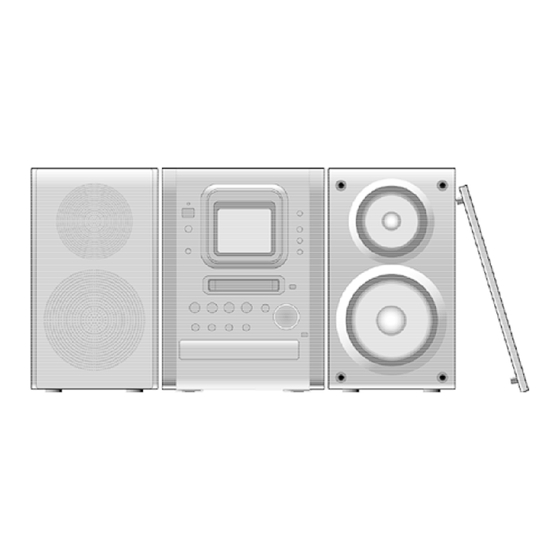
Summary of Contents for Panasonic SA-PM35MD
- Page 1 ORDER NO. MD0102022C3 MD Stereo System SA-PM35MD Colour (W)... White Type Area (GCS)... Singapore TAPE SECTION AR2 MECHANISM SERIES CD SECTION RAE0155Z-1V TRAVERSE DECK SERIES MD SECTION MR3 MECHANISM SERIES SPECIFICATIONS Specification...
- Page 2 Amplifier Section RMS power output THD 10%, both channels driven HIGH 2 X 3 W (6 2 X 15 W (6 Total BI-AMP power 2 X 18 W PMPO (Except for United 320 W Kingdom) Input sensitivity 480 mV P-MD 160 mV Input impedance 25 k...
-
Page 3: Before Repair And Adjustment
Number of channels 2 channels stereo Wow and flutter Below measurable limit CD Section Sampling frequency 44.1kHz Decoding 16 bit linear Beam source Semiconductor laser Wave length 780 nm Number of channels 2 channels stereo S/N ratio SP OUT 70 dB (JIS A) Wow and flutter Below measurable limit Digital filter... - Page 4 The protection circuitry may have operated if either of the following conditions are noticed: - No sound is heard when the power is turned on. - Sound stops during a performance. The function of this circuitry is to prevent circuitry damage if, for example, the positive and negative speaker connection wires are "shorted", or if speaker systems with an impedance less than the indicated rated impedance of the amplifier are used.
- Page 5 4. Handling Precautions For Traverse Deck (CD/MD) The laser diode in the traverse deck (optical pickup) may break down due to potential difference caused by static electricity of clothes or human body. So, be careful of electrostatic breakdown during repair of the traverse deck (optical pickup). Handling of CD traverse deck (optical pickup) 1.
- Page 6 Handling of MD Unit (optical pickup) 1. Do not subject the MD unit (optical pickup) to static electricity as it is extramely sensitive to electrical shock. 2. The short land between the No.25 (LD-GND) and No. 24 (LD) pins on the flexible board is shorted with a solder builder up to prevent damage to the laser diode.
-
Page 7: Precaution Of Laser Diode
Caution when Replacing the Optical Pickup : The traverse has a short point shorted with solder to protect the laser diode against electrostatics breakdown. Be sure to remove the solder from the short point before making connections. 5. Precaution of Laser Diode Caution : This product utilizes a laser diode with the unit turned "ON", invisible laser radiation is emitted from the pick up lens. - Page 8 freigelegten Laserdiode gefährlich ist. 2. Den werkseitig justierten Einstellregler der Lasereinhit nicht verstellen. 3. Nicht mit optischen Instrumenten in die Fokussierlinse blicken. 4. Nicht über längere Zeit in die Fokussierlinse blicken. ADVARSEL : I dette a apparat anvendes laser. CAUTION! THIS PRODUCT UTILIZES A LASER.
-
Page 9: Operation Procedures
6. Operation Procedures... - Page 10 7. Operation Check and Main Component Replacement Procedures “ATTENTION SERVICER” Some chassis components may have sharp edges. Be careful when disassembling and servicing.
- Page 11 1. This section describes procedures for checking the operation of the major printed circuit boards and replacing the main components. 2. For reassembly after operation checks or replacement, reverse the respective procedures.Special reassembly procedures are described only when required. 3. Select items from the following index when checks or replacement are required.
-
Page 12: Checking Procedure For Each Major P.c.b
Einheit ausgetauscht werden. 7.1. Checking Procedure for Each Major P.C.B. 7.1.1. Checking for the Deck P.C.B. Step 1 Remove 4 screws each side. Step 2 Remove 5 screws. Step 3 Lift up the deck unit and push catches each side. - Page 13 - Check the Deck P.C.B. as shown. 7.1.2. Checking for the Transformer P.C.B. - Check the Transformer P.C.B. as shown. 7.1.3. Checking for the Main P.C.B.
- Page 14 Step 6 Remove 2 screws below, push catches each side. - Check the Main P.C.B. as shown. 7.1.4. Checking for the CD Servo P.C.B. Step 2 Lift up the CD unit and place it as shown in the following figure. - Check the CD Servo P.C.B.
- Page 15 Step 2 Remove the CD fixture (B). Step 4 Remove the MD shield and place the MD Servo unit as shown in the following figure. - Check the MD Servo P.C.B. as shown. - When checking the IC1 on the MD Servo P.C.B., it can be measured with test point on the MD Servo P.C.B.
- Page 16 - Check the Power P.C.B. as shown. 7.2. Disassembly and Assembly of the Disc Tray and CD Traverse Unit 7.2.1. Disassembly of the Disc Tray. Step 1 Turn the gear counter clock wise until the CD Tray starts to move out. Step 2 Release the 2 claws and remove the clamp plate in the direction of the arrow.
- Page 17 Step 3 Lift up the CD Tray to remove it. 7.2.2. Disassembly of the CD Traverse Unit. Step 1 Release the 2 claws and remove the CD Traverse Unit in the direction of the arrow. NOTE : 1. Follow the reverse procedure to replace the CD Traverse Unit and CD Tray.
- Page 18 NOTE : When replacing the CD Tray, make sure the Dented line is at the position as shown. 7.3. Main Component Replacement Procedure 7.3.1. Replacement of the CD Servo P.C.B. and Optical Pick-up Unit. Step 2 Desolder the 4 legs of 2 motors and flip over the CD Servo P.C.B. Step 3 Remove the flexible cable at CN701.
- Page 19 NOTE : Insert a short pin into the flexible cable. Step 4 Push the lever in and turn the gear clock wise fully.
- Page 20 Step 6 Release the claw and remove the Driver Plate. Step 7 Slide out the Optical Pick-up Unit from the indent opening. NOTE : Do not touch the Lense on the OPU. 7.3.2. Removal of the Deck P.C.B. and Mechanism P.C.B. for replacing parts.
- Page 21 Step 2 Push the lever upward to open the cassette lid and remove the deck unit. Step 4 Desolder the motor wires. Step 5 Remove the Deck P.C.B. Step 7 Desolder the plunger terminals. Step 8 Release the 4 claws and remove the Mechanism P.C.B.
- Page 22 7.3.3. Replacement for the Magnetic Head and Optical Pick-up. Step 1 Remove the 2 FFCs from the connector. Step 2 Remove the pressure spring from latch. Step 3 Release the 2 claws and then lift up the holder ass’y. Step 4 Set the holder ass’y and MD mechanism unit at a 60 degree angle and then pull out the holder ass’y.
- Page 23 Step 7 Spread the lugs of head shifter and then release the lugs from boss. Step 9 Release the 2 claws and then remove the REF base.
- Page 24 Step 15 Remove the nut plate spring and nut plate. Notice for installing the optical pickup Step 2 Align the guide portion (A) of optical pickup with the sub shaft. Note : Take care not to bend the FFC.
- Page 25 7.3.4. Replacement for the Belt and Loading Motor Assembly Step 4 Release the 4 claws.
- Page 26 Step 7 Release the 2 claws and then lift up the holder ass’y. Note : When installing the holder ass’y, align the lock lever pin with the main rack slot. Step 8 Set the holder ass’y and MD mechanism unit at a 60 degree angle, and then pull out the holder ass’y.
- Page 27 - Align the hole of loading motor with the boss of mechanism chassis and then install the loading motor. 7.3.5. Replacement for the Traverse Motor Assembly - Follow Step 1 ~ Step 8 of item 1.3.4 in Main Component Replacement Procedures. Step 3 Spread the lugs of head shifter and then release the lugs from boss.
-
Page 28: Self-Diagnostic Display Function
Notice for installing the traverse motor - Align the hole of traverse motor with the boss of mechanism chassis and then install the traverse motor. 8. Self-Diagnostic Display Function This unit is equipped with a self-diagnostic function which, in the event of a malfunction, automatucally display a code indication the nature of the malfunction. - Page 29 still pressing the STOP button, press the Forward Skip/Search button for at least 2 seconds. The unit enters Self-Diagnostic Mode and display “TEST”. Then an error code (e.g. H01) is displayed, if any. In the case of no error, “TEST” is displayed on 4.
- Page 30 8.5.1. Power Amplifier Failure (F76) When power amplifier output failure for power supply failure. 8.5.2. Error detection for CD Block Error Code Problem Condition Possible Cause CD does not function REST SW detection error. This error occurs when the Optical Pick Up REST SW (S701) detected within the specified time.
-
Page 31: Measurement And Adjustment
Error Code Problem Condition Possible Cause Cassette deck MODE SW detection error. maifunctions Faulty contact or short circuit of mechanism mode switch. ( Recording not possible REC INH SW detection error. Faulty contact or short circuit of REC INH switch. (S974, S975) Playback cannot HALF SW detection error. - Page 32 1. Connect the measuring instrument as shown in Fig. 2. 2. Replace azimuth screws for both forward and reverse direction after removing the screw-locking bond left on the head base. (Supply part No. of azimath adjusting screw: RHD17015) 3. Playback the azimuth adjustment portion(8kHz, -20dB) of test tape(QZZCFM).
- Page 33 9.1.2. Tape Speed Adjustment Normal speed (Standard value : 3000 ± 90Hz) 1. Connect the measuring instrument as shown in Fig. 4. 2. Playback the middle portion of the test tape (QZZCWAT). 3. Adjust motor VR for the output value shown below. (Refer to Fig. [Adjustment target : 3000 ±...
-
Page 34: Tuner Section
[Standard value : 16 ± 3mV] Fig. 6 9.1.4. Bias Frequency Check 1. Connect the measuring instrument as shown in Fig. 7. 2. Set the unit to “AUX” position. 3. Insert the normal blank tape (QZZCRA) and set the unit to “REC” mode (use “... -
Page 35: Alignment Points
SIGNAL GENERATOR or SWEEP RADIO DIAL INDICATOR ADJUSTMENT REMARKS GENERATOR SETTING (ELECTRONIC (Shown in Fig. 3) VOLTMETER or CONNECTIONS FREQUENCY OSCILLOSCOPE) Fashion a loop 522kHz Tuning capacitor Headphones Z101 (AM OSC Adjust of several turns fully closed Jack (32 Coil) maximum of wire and (Fabricate the... -
Page 36: Laser Power Adjustment
Fig. 10 9.4. Laser Power Adjustment djust each laser power : read power for reading (play) and write power for writing (record). 9.4.1. Necessary Instruments - Laser power meter (Advantest TQ8210 or compatible meter) - Test disc (Pre-mastered disc RFKV0006 or RFKV0014) - Recordable disc available on sales root (with music recorded) - Insulated driver for adjustment such as a ceramic driver - Jitter meter... - Page 37 1. About handling the MD unit - The magnetic head is a precision unit and is very fragile. Do not deform it. - Laser diode in the optical pickup may be destroyed by the staticelectricity generated in your clothes or body. Be especially careful with the static electricity.
- Page 38 MD loaded. Doing so may result in damage to the MD. 9.4.3. Adjustment Procedure 1. Enter “1” using numeric pad on the remote control with no MD loaded. FL display “Rough ADJ”. (Read power adjustment mode) 2. Slide sensor cover on the laser power meter. (Fig. 1) 3.
- Page 39 next indication. FL display “FINE ADJ” (Write power adjustment mode) 6. Adjust VR1 until reading of the laser power meter is within the standard value. (Fig. 3) [Standard value (write power) : 6.8mW ± 0.1mW] Cautions Do not allow the write power to reach or exceed 7.5mW, even for a moment.
- Page 40 The unit returns to the state same as shipping from the factory. (Memories such as preset broadcasting station will be lost.) 10. Illustration of IC’s, Transistors and Diodes 11. Terminal Function of IC's 11.1. IC1 (AN8772FHQ) : RF AMP Mark Function CENVD —...
- Page 41 Mark Function TGAIN Tracking gain adjustment input terminal Lens position signal output terminal AB GAIN APP compensation signal gain adjustment terminal Focus error signal output terminal AS GAIN AS gain adjustment terminal FBAL Focus ballance adjustment terminal AS/3TMON signal output MON3T terminal 3T envelope det.
- Page 42 Mark Function VREF Reference voltage output terminal RF1 signal input terminal RF2 signal input terminal F1 signal input terminal F2 signal input terminal CLPF1 — APP compensation LPF capacitor connection terminal CLPF2 — RF equalizer adjustment resistor connection terminal Beam A~D signal input terminal CENVC —...
- Page 43 Mark Function VO4+ Tracking coil driver output terminal VO3- Focus coil driver output terminal VO3+ Focus coil driver output terminal VO2- Traverse motor drive output terminal VO2+ Traverse motor drive output terminal VO1- Spindle motor drive output terminal VO1+ Spindle motor drive output terminal PGND1 —...
- Page 44 Mark Function ADIP ADIP FM signal input terminal Lens position signal input terminal Focus error signal input terminal Tracking error signal input terminal AS signal input terminal DRMONI Drive voltage monitor input terminal Battery power supply terminal AMONI — Servo analog monitor signal output (Not used, poen) VREFI Reference voltage input...
- Page 45 FG input terminal Mark Function NRECT Rec/Play switching signal output terminal IVDD2 — Power supply terminal for I/ O pad IVDD0 — Power supply terminal for I/ O pad DVss0 — GND terminal RAD12 — DRAM address output terminal (Not used, open) ~RAD10 RAD9 DRAM address output...
- Page 46 Mark Function CD bit clock input terminal (Connected to GND) DATA CD data input terminal (Connected to GND) Digital audio interface signal output terminal (Not used, open) Digital audio interface signal 1 input terminal Digital audio interface signal 2 input terminal NREFM —...
- Page 47 Mark Function APCD Laser power PWM output terminal 93 EXEFMCK External FM clock input terminal (Not used, connected to GND through registor) PEFM1 EFM loop filter output terminal EFM PLL reference current EEMIREF input terminal 96 EEMPLLF EFM PLL filter output terminal PEFMS EFM signal input terminal...
- Page 48 Mark Function TVSW Traverse innermost detection switch signal input terminal DISC IN Disc detection switch signal input terminal Reflection rate switch REFLECT signal input terminal LOAD Loading mechanism position det. Switch 0 (OPEN) signal input terminal LOAD Loading mechanism position det. Switch 1 (TRG) signal input terminal LOAD...
- Page 49 Mark Function OSC2 O Crystal oscillator output terminal (f=10.02MHz) — GND terminal Not used, connected to GND O Not used, open — GND terminal TEST03 O Test signal output terminal (Not used, open) EEPCS O EEPROM chip select signal output terminal (Not used, open) EEPCK O EEPROM clock signal...
- Page 50 data output terminal Mark Function LCDCK O LCD clock test signal output terminal (Connected to power supply through resistor) ADRS O Test signal output terminal TEST (Connected to power supply through resistor) O Test signal output terminal DATA (Not used, open) VREF- —...
- Page 51 Mark Function BUSY O Servo busy test signal output terminal (Not used, open) 77 SBPRETRY O Signal management retry test signal output terminal (Not used, open) 78 SRVRETRY O Servo retry test signal output terminal (Not used, open) ARDSKIP O Address skip test signal output terminal (Not used, open) SPMWE...
- Page 52 Mark Function — GND terminal 11.6. IC701 (AN8839NSBE2) SERVO AMPLIFIER Mark Function Tracking signal input terminal 1 (E ch) Tracking signal input termianl 2 (F ch) Power supply connection Focus signal input termianl 1 (A ch) Focus signal input terminal 2 (B ch) Laser PD connection Laser power auto control...
- Page 53 Mark Function VREF Reference voltage output TBAL Tracking balance signal input FBAL Focus balance signal input 11.7. IC702 (MN662790RSC) SERVO PROCESSOR / DIGITAL SIGNAL PROCESSOR / DIGITAL FILTER / D/A CONVERTER Pin No. Mark I/O Function BCLK Bit Clock Output for Serial Data LRCK L/P Clock Signal Output...
- Page 54 Pin No. Mark I/O Function SQCK External Clock Signal Input for Sub-Code Q Resistor) SUBQ Sub-Code Q Code Output DMUTE Muting Input (“H”: Mute) STAT Status Signal Output (CRC, CUE, CLVS, TTSTVP, FCLV, SQCK) /RST Reset Signal Input SMCK 1/2 - Divided Clock Signal of Crystal Oscillating at MSEL= “H”...
- Page 55 Adjustment Output Pin No. Mark I/O Function Focus Error Signal Input (Analog Input) Tracking Error Signal Input (Analog Input) RFENV RF Envelope Signal Input VDET Vibration Detection Signal Input (“H”: Detect) Off-Track Signal Input (“H”: Off Track) TRCRS Track Cross Signal Input) /RFDET RF Detection Signal...
- Page 56 Pin No. Mark I/O Function PLL Extraction Clock Output (Not Used, Open) (fPCK= 4.3218 MHz during Normal Playback) VCOF2 I/O VCO loop Filter for 33.8688 MHz Conversion Terminal for 16.9344 Mhz Crystal mode, Must use other Circuit) SUBC Sub-Code Serial Data Output (Not Used, Open) SBCK...
- Page 57 Pin No. Mark I/O Function CLVS Spindle Servo Phase Synchronizing Signal Output (“H”: CLV, “L”: Rough Servo) (Not used, Open) Sub-Code CRC Checked Output (“H”: OK, “L” NG) (Not Used, Open) DEMPH De-Emphasis DN Signal Output (“H”:ON) RESY Frame Re- synchronizing Signal Output IOSEL...
- Page 58 Mark I/O Function Motor Driver 92) Input Turntable Motor Drive Signal (“L”:ON) Motor Driver (1) Input — Traverse Motor Drive Signal (“L”:ON) N.C. — No connection N.C. — No connection N.C. — No connection N.C. — No connection PGND1 — Ground Conenction (1) for Driver PVCC1 Power Supply (1) for...
- Page 59 11.9. IC801 (M30622MC4A3F) SYSTEM MICROPROCESSOR Pin No. Mark I/O Function CD_MLD O CD command load output CD_RST O CD reset output CD_MCLK O CD command clock output CD_MDATA O CD command data output CD_RESTSW CD limit detect sw input MBP1 O Control output (H=ON) MBP2 O Control output (H=ON)
- Page 60 Pin No. Mark I/O Function SUBQ/SRDT CD subcode clock input SQCK/SCLK O CD subcode clock output LOAD SW MD load (TRG) SW (H:SW off) MD_LINK O MD portable link serial data output MD_LINK IN MD portable link serial data input CR02 PB O CR02 tape play back (active H)
- Page 61 Pin No. Mark I/O Function OPEN_H O CD open tray normal (Active : H) — Power supply 5.0V N.C. O No connection — GND (0V) N.C. O No connection TAPE_EJ Tape eject key N.C. O No connection N.C. O No connection LD_SPD CD loading speed select...
- Page 62 Pin No. Mark I/O Function AVSS — Analog power supply input SETUP AD Setup tuner band TUNER BAND VREF reference voltage input AVCC — Analog power supply input N.C. O No connection 12. Block Diagram 13. Schematic Diagram (All schematic diagrams may be modified at any time with the development of new technology) Note : PROTECT detect switch REFLECT detect switch...
- Page 63 S922 Display / Character switch S923 Rec Mode switch S924 MD and Tape Rec switch S925 Tape Rec switch S926 MD Rec switch S932 CD Open / Close switch S933 MD Eject switch S934 Stop switch S935 FF switch S936 Rew switch S937 Selector switch...
- Page 64 S950 Tape Eject switch S971 Mode detect switch S972 Leaf switch S973 Leaf switch S974 Leaf switch S975 Leaf switch S780 CD Open switch Laser power adjust VR VR901 Volume control VR Signal line : +B line : -B line : FM/AM signal line : Main signal line : Playback signal line...
- Page 65 : Record signal line : FM signal line : AM signal line : AM OSC signal line : FM OSC signal line : AUX signal line : CD signal line : MD signal line : MD record signal line - The voltage value and waveforms are the reference voltage of this unit measured by DC electronic voltmeter (high impedance) and oscilloscope on the basis of chassis.
-
Page 66: Printed Circuit Board
(( )) : CD < > : FM : AM (for MD Servo Circuit) : MD play [1kHz, L+R, 0dB] < > : MD rec. [1kHz, L+R, 0dB] : MD - Importance safety notice : Components identified by mark have special characteristics important for safety. -
Page 67: Troubleshooting Guide
16. Troubleshooting Guide... -
Page 74: Parts Location And Replacement Parts List
17. Parts Location and Replacement Parts List Notes: - Important safety notice: Components identified by mark have special characteristics important for safety. Furthermore, special parts which have purposes of fire-retardent (resistors), high-quality sound (capacitors), low noise (resistors), etc are used. When replacing any of these components, be sure to use only manufacturer’s specified parts shown in the parts list. - Page 75 - Die Lasereinheit darf nur gegen eine vom Hertsteller spezifizierte Einheit ausgetauscht werden. - Capacitor values are in microfarads ( F) unless specified otherwise, P= Pico-farads (pF), F= Farads. - Resistance values are in ohms, unless specified otherwise, 1K= 1,000 (OHM). - The marking (RTL) indicates that the Retention Time is limited for this items.
- Page 76 17.1.2. Deck Mechanism Parts List...
- Page 77 Ref. No. Part No. Part Name & Description Remarks CASSETTE DECK RED0043 R/P HEAD BLOCK UNIT 101-1 RHD17015 SCREW RDG0300 REEL BASE GEAR RDG0301 WINDING RELAY GEAR RDK0026 MAIN GEAR RDV0033-4 WINDING BELT RDV0034-1 CAPSTAN BELT ‘A’ RMB0312 TRIGGER LEVEL SPRING RMB0400 REEL SPRING RMB0403...
- Page 78 17.2.2. MD Mechanism Parts List...
-
Page 79: Cd Loading Mechanism
Ref. No. Part No. Part Name & Description Remarks TRAVERSE DECK RED0047-2 RECORDING HEAD RHD17021 NUT PLATE SCREW RHD17022 RECORDING HEAD SCREW RMC0348 THRUST SPRING RMC0349 NUT PLATE SPRING RML0515 HEAD SHIFTER RMQ0750 REF BASE RMQ0751 NUT PLATE RMS0611 MAIN SHAFT RXJ0021 DRIVE SHAFT ASS’Y RXK0249... - Page 80 17.3.2. CD Mechanism Parts List...
- Page 81 Ref. No. Part No. Part Name & Description Remarks TRAVERSE DECK RAE0155Z-1V CT100W TRAVERSE RDG0455 TRAVERSE GEAR (A) RDG0456 TRAVERSE GEAR (B) RFKNCT100 TRAVERSE BASE ASS’Y 304-1 RDG0457 LOAD GEAR (A) 304-2 RDG0458 LOAD GEAR (B) 304-3 RDG0459 LOAD GEAR (C) 304-4 RME0290 PRESS SPRING...
- Page 83 17.4.2. Cabinet Parts List...
- Page 84 Ref. No. Part No. Part Name & Description Remarks CABINET AND CHASSIS REEX0098 30P FFC XTB3+8JFZ SCREW XTV26+5F TAPPING SCREW M26X6 RGUX0359-W CASS EJECT BUTTON RHD26016 SCREW (PHONE JACK) RKMX0055-S TOP CABINET RGPX0035-S CASS LID RMBX0014 CASS OPEN SPRING XTBS26+10J SCREW XTV3+10G SCREW...
-
Page 85: Electrical Part List
Ref. No. Part No. Part Name & Description Remarks REXX0232 9P TRANS TO POWER RMKX0042-1 BOTTOM CHASSIS RSCX0045 TUNER REAR SHIELD RSCX0046 MD SHIELD RSC0027-L SHIELD CASE RUS757ZAA CASS HALF SPRING RWJ0102050KR MOTOR WIRE RWJ0206150RR 6 PIN POWER AMP TO H RWJ0207215XR 7 PIN MAIN TO MD LIN RWJ0211090XQ... -
Page 86: Integrated Circuits
Ref. No. Part No. Part Name & Description Remarks PRINTED CIRCUIT CIRCUITS REP2895A-T MD SERVO P.C.B. SIDE A [M]RTL REP2895A-T MD SERVO P.C.B. SIDE B [M]RTL REP2807C CD SERVO P.C.B. [M]RTL REPX0227C MAIN P.C.B. [M]RTL REPX0228C SPEAKER P.C.B. [M]RTL REPX0226A FL P.C.B. - Page 87 Ref. No. Part No. Part Name & Description Remarks IC601 UPC29M33HF IC701 AN8839NSBE2 IC HEAD AMP IC702 MN662790RSC IC LSI IC703 BA5948FPE2 IC 4 CH DRIVE IC801 M30622MC4A3F IC MICOM IC802 TC74HCT7007A IC 3V TO 5V IC902 BU2090AF-E2 IC I/O EXPANDER IC971 0N2180RLC1 PHOTO INTERUPTOR...
- Page 88 Ref. No. Part No. Part Name & Description Remarks Q618 KTA1046 TRANSISTOR Q619 KTC3199GRTA TRANSISTOR Q620 KRA110MTA TRANSISTOR Q701 2SA1037AKSTX TRANSISTOR Q701 KTC3875GRTA TRANSISTOR Q702 DTC143XKA146 TRANSISTOR Q702 KTA1504GRTA TRANSISTOR Q703 DTA143XKA146 TRANSISTOR Q703 KTC3875GRTA TRANSISTOR Q803 KRC104STA TRANSISTOR Q901 KRA119MTA TRANSISTOR Q902...
- Page 89 Ref. No. Part No. Part Name & Description Remarks SVC211SPA-AL DIODE SVC211SPA-AL DIODE SVC211SPA-AL DIODE SC80209TE12R DIODE SC80209TE12R DIODE MA728TX DIODE D101 UDZSTE175R1B DIODE D103 RL1N4003N02 DIODE D401 1SS355TE17 DIODE D534 RVD1SS133TA DIODE D535 RVD1SS133TA DIODE D538 RVD1SS133TA DIODE D542 RB441Q40T77 DIODE D545...
- Page 90 Ref. No. Part No. Part Name & Description Remarks D809 RL1N4003N02 DIODE D901 NSPW510BS DIODE D902 NSPW510BS DIODE D903 NSPW510BS DIODE D904 SLR325MCT31W DIODE D905 SLR325MCT31W DIODE D906 SLR325MCT31W DIODE D907 SML79455C DIODE D908 SML79455C DIODE D909 SML79455C DIODE D910 SML79455C DIODE D911...
- Page 91 Ref. No. Part No. Part Name & Description Remarks S938 EVQ21405R SW SOUND EQ S939 EVQ21405R SW CD S940 EVQ21405R SW MD S941 EVQ21405R SW TAPE S942 EVQ21405R SW TUNER S950 EVQ21405R SW DECK OPEN S971 RSH1A018-3U MODE SWITCH S972 RSH1A019-2U SW, LEAF S973...
- Page 92 Ref. No. Part No. Part Name & Description Remarks RLQU101KT-W CHIP COIL RLQU2R2MT-W CHIP COIL RLQU2R2MT-W CHIP COIL RLQU2R2MT-W CHIP COIL RLQU2R2MT-W CHIP COIL RLQU2R2MT-W CHIP COIL RLQU100KT-W CHIP COIL RLQU100KT-W CHIP COIL RLQU100KT-W CHIP COIL RLQU100KT-W CHIP COIL RLQU2R2MT-W CHIP COIL RLQU2R2MT-W CHIP COIL...
- Page 93 Ref. No. Part No. Part Name & Description Remarks OSCILLATORS RSXY10M0M02T CRYSTAL OSCILLATOR RSXC16M9S03T CRYSTAL OSCILLATOR X102 RLFDFT22DD CRYSTAL OSCILLATOR X103 RSXC7M20S05T CRYSTAL OSCILLATOR X701 RSXC33M8S01 CRYSTAL OSCILLATOR X801 RSXZ8M00D01T CERAMIC RESONATOR X802 RSXD32K0C01 CRYSTAL OSCILLATOR FUSES F601 XBA2C06TB0 FUSE FUSE HOLDERS FC601 EYF52BC...
- Page 94 Ref. No. Part No. Part Name & Description Remarks PW1301 RMR0320 HOLDER PW1303 RMR0317 8P WIRE HOLDER RESISTORS ERDS2TJ104T 100K 1/4W ERJ3GEYJ472V 4.7K 1/16W ERDS2TJ104T 100K 1/4W ERJ3GEYJ102V 1K 1/16W ERDS2TJ221T 220 1/4W ERJ3GEYJ472V 4.7K 1/16W ERDS2TJ104T 100K 1/4W ERDS2TJ564T 560K 1/4W ERJ3GEYJ1R0V 1 1/16W ERDS2TJ391T...
- Page 95 Ref. No. Part No. Part Name & Description Remarks ERJ3GEYJ222V 2.2K 1/16W ERJ3GEYJ473V 47K 1/16W ERJ3GEYJ102V 1K 1/16W ERJ3GEYJ332V 3.3K 1/16W ERJ3GEYJ223V 22K 1/16W ERJ3GEYJ682V 6.8K 1/16W ERJ3GEYJ683V 68K 1/16W ERJ3GEYJ332V 3.3K 1/16W ERJ3GEYJ223V 22K 1/16W ERJ3GEYJ223V 22K 1/16W ERJ3GEYJ103V 10K 1/16W ERJ3GEYJ471V 470 1/16W ERJ3GEYJ471V 470 1/16W ERJ3GEYJ471V 470 1/16W...
- Page 96 Ref. No. Part No. Part Name & Description Remarks R111 ERJ3GEYJ221V 220 1/16W R111 ERJ6GEYJ391V 390 1/10W R112 ERJ3GEYJ221V 220 1/16W R112 ERJ6GEYJ104V 100K 1/10W R113 ERJ6GEYJ103V 10K 1/10W R114 ERJ3GEYJ103V 10K 1/16W R114 ERJ6GEYJ562V 5.6K 1/10W R115 ERJ3GEYJ103V 10K 1/16W R115 ERJ6GEYJ561V 560 1/10W R116...
- Page 97 Ref. No. Part No. Part Name & Description Remarks R146 ERJ6GEYJ472V 4.7K 1/10W R147 ERJ3GEYJ102V 1K 1/16W R151 ERJ6GEYJ820V 82 1/10W R152 ERJ6GEY0R00A 0 1/10W R174 ERJ3GEYJ103V 10K 1/16W R401 ERJ6GEYJ223V 22K 1/10W R402 ERJ6GEYJ223V 22K 1/10W R403 ERJ6GEYJ182V 1.8K 1/10W R404 ERJ6GEYJ182V 1.8K 1/10W R409...
- Page 98 Ref. No. Part No. Part Name & Description Remarks R462 ERJ6GEYJ473V 47K 1/10W R463 ERJ6GEYJ102V 1K 1/10W R464 ERJ6GEYJ335V 3.3M 1/10W R465 ERJ6GEYJ103V 10K 1/10W R466 ERJ6GEYJ105V 1M 1/10W R467 ERJ6GEYJ822V 8.2K 1/10W R468 ERJ6GEYJ822V 8.2K 1/10W R469 ERJ6GEYJ823V 82K 1/10W R471 ERJ6GEYJ822V 8.2K 1/10W R481...
- Page 99 Ref. No. Part No. Part Name & Description Remarks R622 ERD2FCVG220T 22 1/4W R623 ERDS2TG152T 1.5K 1/4W R624 ERDS2TG152T 1.5K 1/4W R627 ERDS2TJ221T 220 1/4W R628 ERDS2TJ221T 220 1/4W R629 ERDS2TJ561T 560 1/4W R630 ERDS2TJ104T 100K 1/4W R631 ERDS2TJ104T 100K 1/4W R633 ERDS2TJ222T 2.2K 1/4W...
- Page 100 Ref. No. Part No. Part Name & Description Remarks R735 ERJ6GEYJ101V 100 1/10W R736 ERJ6GEYJ101V 100 1/10W R741 ERJ6GEYJ473V 47K 1/10W R742 ERJ6GEYJ224V 220K 1/10W R744 ERJ6GEYJ124V 120K 1/10W R749 ERJ6GEYJ272V 2.7K 1/10W R750 ERJ6GEYJ151V 150 1/10W R751 ERJ6GEYJ562V 5.6K 1/10W R752 ERJ6GEYJ222V 2.2K 1/10W R753...
- Page 101 Ref. No. Part No. Part Name & Description Remarks R840 ERJ6GEYJ474V 470K 1/10W R841 ERJ6GEYJ102V 1K 1/10W R842 ERJ6GEYJ102V 1K 1/10W R846 ERJ6GEYJ102V 1K 1/10W R847 ERJ6GEYJ223V 22K 1/10W R848 ERJ6GEYJ153V 15K 1/10W R849 ERJ6GEYJ101V 100 1/10W R855 ERJ6GEYJ104V 100K 1/10W R856 ERJ6GEYJ103V 10K 1/10W R857...
- Page 102 Ref. No. Part No. Part Name & Description Remarks R934 ERDS2TJ182T 1.8K 1/4W R935 ERDS2TJ101T 100 1/4W R936 ERDS2TJ102T 1K 1/4W R940 ERDS2TJ101T 100 1/4W R941 ERDS2TJ102T 1K 1/4W R942 ERDS2TJ122T 1.2K 1/4W R943 ERDS2TJ102T 1K 1/4W R944 ERDS2TJ182T 1.8K 1/4W R945 ERDS2TJ272T 2.7K 1/4W...
- Page 103 Ref. No. Part No. Part Name & Description Remarks R1102 ERDS2TJ153T 15K 1/4W R1103 ERDS2TJ560T 56 1/4W R1104 ERDS2TJ681T 680 1/4W R1105 ERDS2TJ103T 10K 1/4W R1107 ERDS2TJ334T 330K 1/4W R1109 ERDS2TJ273T 27K 1/4W R1110 ERDS2TJ222T 2.2K 1/4W R1111 ERDS2TJ122T 1.2K 1/4W R1112 ERDS2TJ470T 47 1/4W...
- Page 104 Ref. No. Part No. Part Name & Description Remarks R1329 ERDS2TJ335T 3.3M 1/4W R1330 ERDS2TJ823T 82K 1/4W R1331 ERDS2TJ104T 100K 1/4W R1332 ERDS2TJ333T 33K 1/4W R1333 ERDS2TJ472T 4.7K 1/4W R1334 ERDS2TJ393T 39K 1/4W R1335 ERDS2TJ682T 6.8K 1/4W R1336 ERDS2TJ681T 680 1/4W R1337 ERDS2TJ473T 47K 1/4W...
- Page 105 Ref. No. Part No. Part Name & Description Remarks ECUVNC393KBV 0.039 16V ECUV1H472KBV 4700P 50V ECUV1A106ZFM 10 10V ECUV1H332KBV 3300P 50V ECUV1E123KBV 0.012 25V ECUV1H102KBV 1000P 50V ECUV1H102KBV 1000P 50V ECUV1C475ZFM 47 16V ECUV1H102KBV 1000P 50V ECUV1H102KBV 1000P 50V ECUV1H181KCV 180P 50V ECUVNC104ZFV 0.1 16V ECEV0JA331P 330 6.3V...
- Page 106 Ref. No. Part No. Part Name & Description Remarks ECUVNC104ZFV 0.1 16V ECUV1H102KBV 1000P 50V C101 ECUV1A106ZFM 10 10V C101 ECUV1H103KBN 0.01 50V C102 ECA1CAK470XB 47 16V C102 ECUVNC104ZFV 0.1 16V C103 ECUV1A106ZFM 10 10V C103 ECUV1H103KBN 0.01 50V C104 ECUV1H102KBN 1000P 50V C106 ECUV1H102KBV 1000P 50V...
- Page 107 Ref. No. Part No. Part Name & Description Remarks C136 ECUV1H102KBN 1000P 50V C137 ECUV1H332KBN 3300P 50V C138 ECEV0JA470SR 47 6.3V C138 ECUV1H103KBN 0.01 50V C139 ECEA1EKA4R7B 4.7 25V C139 ECUVNC104ZFV 0.1 16V C140 ECUVNC104ZFV 0.1 16V C141 ECA1HAK010XB 1 50V C141 ECUVNC104ZFV 0.1 16V C142...
- Page 108 Ref. No. Part No. Part Name & Description Remarks C435 ECUV1H222KBN 2200P 50V C436 ECUV1H222KBN 2200P 50V C437 ECA1CAK100XB 10 16V C438 ECA1CAK100XB 10 16V C440 ECA1HAKR47XB 0.47 50V C441 ECA1HAKR47XB 0.47 50V C442 ECQV1H154JZ3 0.15 50V C443 ECUV1H471JCV 470P 50V C444 ECFR1C473KR 0.047 16V...
- Page 109 Ref. No. Part No. Part Name & Description Remarks C547 ECA1CAK101XB 100 16V C550 ECBT1H221KB5 220P 50V C555 ECA1HAK010XB 1 50V C557 ECA1EAK330XB 33 25V C589 ECBT1H473ZF5 0.047 50V C590 ECBT1H473ZF5 0.047 50V C591 ECEA1AKA221Q 220 10V C592 ECEA1AKA221Q 220 10V C603 ECA1HM470B 47 50V...
- Page 110 Ref. No. Part No. Part Name & Description Remarks C714 ECEA0JKA101I 100 6.3V C715 ECUV1H272KBN 2700P 50V C716 ECUV1H821KBN 820P 50V C717 ECUV1E104ZFN 0.1 25V C718 ECUV1C224KBN 0.22 16V C723 ECEA1AKA221I 220 10V C724 ECUV1E104MBN 0.1 25V C725 ECUV1H102KBN 1000P 50V C726 ECUV1H102KBN 1000P 50V C727...
- Page 111 Ref. No. Part No. Part Name & Description Remarks C820 ECEA1CKA100B 10 16V C821 ECUV1H101KCN 100P 50V C822 ECUV1H101KCN 100P 50V C823 ECUV1H101KCN 100P 50V C824 ECUV1H101KCN 100P 50V C825 ECUV1H101KCN 100P 50V C826 ECEA1AKA220B 22 10V C827 ECUV1H103KBN 0.01 50V C828 ECUV1H102KBN 1000P 50V C829...
- Page 112 Ref. No. Part No. Part Name & Description Remarks C1208 ECEA0JKA470B 47 6.3V C1211 ECA1HAK4R7XB 4.7 50V C1212 ECBT1H102KB5 1000P 50V C1213 ECBT1H102KB5 1000P 50V C1214 ECBT1H102KB5 1000P 50V C1215 ECBT1H101KB5 100P 50V C1216 ECBT1C682KR5 6800P 16V C1301 ECEA1HN010SB 1 50V C1303 ECBT1C103MS5 0.01 16V C1305...
-
Page 113: Packaging Materials & Accessories Parts List
17.6. Packaging Materials & Accessories Parts List Ref. No. Part No. Part Name & Description Remarks PACKING MATERIALS RPGX0692 PACKING CASE RPNX0120 POLYFOAM RPHV0001 MIRAMAT SHEET ACCESSORIES RAK-SC971WK REMOTE CONTROL A1-1 RXQX0008-W R/C BATTERY COVER RJA0019-2K AC CORD (SF) RQT5600-B O/I BOOK (EN) RQT5601-K O/I BOOK (CH) - Page 114 Printed in Singapore / P010200001 J/E/H/K/L/PRT...
- Page 115 MD SERVO P.C.B SIDE-B (REP2895A-T) R122 R130 C112 R104 R121 R132 R116 C142 R134 R117 R125 R135 C141 R124 IC72 C100 C101 C143 R131 C103 R109 C149 C122 C148 C144 R112 C147 C117 R111 C133 S D G ELECTRICAL PARTS LOCATION Ref.
- Page 116 DECK P.C.B. (REPX0228C) PW1301 R1330 J1015 Q1330 R1111 C1116 J1017 R1324 R1323 J1007 R1214 R1114 C1318 Q1204 R1110 Q1205 Q1201 R1210 R1322 IC1303 R1209 Q1101 R1337 R1398 Q1319 W1981 R1109 J1001 R1336 Q1304 Q1202 C1106 Q1318 R1395 R1103 IC1301 C1320 C1319 J1014 J1016...
- Page 117 MAIN P.C.B. (REPX0227C) C134 X103 R137 R136 R135 R134 R133 R117 R138 CN1303 CP910 CN1301 C122 Q703 J115 R122 J103 C121 C141 J104 R870 R766 J105 C426 R871 R424 R141 R860 R872 R858 C139 R859 R849 R873 C832 R142 R123 C142 R874 R143...
- Page 118 C111 C125 C130 R111 R115 R113 R114 Z120 (TUNER PACK) C110 R151 R129 C124 R105 R132 R127 C103 J904 Q101 C129 C149 C107 C108 R112 R106 R107 3 5 4 7 3 6 C126 R126 R125 R109 C127 C114 C136 R119 R446 R448...
- Page 119 DECK MECHANISM P.C.B (REPX0108) S973 Z971 CS971 1 2 3 4 5 6 7 8 9 S971 S975 S974 S972 D971 IC971 SOLENOID HEADPHONE P.C.B MD SWITCH P.C.B (REPX0228C) (REP2575A) PHONES P-MD TRGSW1 1 2 3 4 5 6 7 8 9 OPENSW0 REFLECT JK503...
- Page 120 PANEL P.C.B. (REPX0226A) WH905A R980 J943 J941 D916 J942 R931 S920 C933 POWER REC MODE C934 R932 J910 S924 J912 Z902 MD&TAPE REC S925 CN901B C915 TAPE REC R930 C914 R934 S922 J909 MD REC DISP/CHAR J915 R992 R991 C912 Q902 R971 C913...
- Page 121 POWER P.C.B. (REPX0228C) R622 Q605 Q613 WH505 D616 C624 J510 R611 R621 C622 C520 R519 C625 R614 C555 D615 D627 R616 C519 R520 R521 D617 R536 D546 D534 C514 C634 R564 R638 J633 J558 R633 C547 J503 C635 Q619 D621 J571 J509 J572...
- Page 122 CD SERVO P.C.B (REP2807C) (RF) TJ701 C727 X701 TJ701 TP19 C725 R714 C716 C726 TP16 C717 C728 R709 TP17 C702 TP26 C744 TP24 R712 C724 TP25 C723 TP18 TP35 TP27 Q703 TP13 IC701 R721 TP14 J723 C730 C732 TP11 Q702 C711 J726 IC702...
- Page 123 SPEAKER P.C.B. (REPX0228C) JK501 CN503B CN502B C526 J152 J151 J150 J153 J850 J751 J750 JK502 CN501A CN503C CN502C 12 11 10 9 FL P.C.B. (REPX0226A) WH905B 1 2 3 4 5 6 7 8 C925 Z901 2 3 4 5 6 7 8 9 L901 Q909 D917...
- Page 124 TRANSFORMER P.C.B. (REPX0228C) CAUTION RISK OF ELECTRIC SHOCK AC VOLTAGE LINE. PLEASE DO NOT TOUCH THIS P.C.B J619 Q602 FC601 FC602 JK601 Q604 D613 J613 R605 F601 250V T630mA J612 R613 C605 AC IN L601 Q603 R612 230V-240V B C E 50HZ J611 D611...
- Page 125 SCHEMATIC DIAGRAM-7 CD SERVO CIRCUIT : +B signal line : CD Signal line TJ701 Q701 2SA1037AKSTX LASER POWER DRIVE OPTICAL PICKUP CIRCUIT C703 6.3V100 CN701 C704 Q701 LASER DIODE R754 C714 6.3V100 LD GND NBOUT GND(GUARD) C713 NAOUT VREF VREF GND(GUARD) IC701 IC701...
-
Page 126: Schematic Diagram
SCHEMATIC DIAGRAM-8 : +B signal line : CD Signal line C727 R717 50V1 C728 R718 50V1 C731 6.3V220 C730 C754 470P High Speed Version (RAD3512) 33.8688MHz RSXC33M8S01 X701 R714 C723 6.8K 10V220 C724 61 62 63 64 65 66 67 68 69 70 71 72 73 74 75 76 77 78 79 80 BYTCK LRCK SRDATA... -
Page 127: Deck Circuit
SCHEMATIC DIAGRAM-12 DECK CIRCUIT :+B signal line :Record signal line :Playback signal line Q1102,Q1202 Q1101,Q1201 R1328 2SJ498CTA 2SJ498CTA HEAD SELECT(REC:ON) HEAD SELECT(PLAY:ON) R1107 R1207 330K 330K Q1201 CP1301 R1105 C1105 C1205 R1205 <<9.1V>> 0.015 0.015 C1103 R1103 C1203 6.3V47 6.3V47 Erase Q1101 C1104... - Page 128 SCHEMATIC DIAGRAM-13 :+B signal line :Record signal line :Playback signal line R1319 R1309 R1334 R1326 R1308 6.8K C1324 P.B.Rch 4700P C1323 C1317 0.01 R1335 5.1V 5.1V 5.1V 10V R1307 Q1330 6.8K R1105 KTC3199GRTA R1320 P.B.Lch TPS DRIVE IC1303 C1103 R1103 6.3V47 BA4558FE2 2.5V...
-
Page 129: Main Circuit
SCHEMATIC DIAGRAM-9 : +B signal line : FM signal line : FM OSC signal line : FM/AM signal line : AM signal line : AM OSC signal line : Playback signal line : MD signal line : Record signal line : AUX signal line MAIN CIRCUIT : MAIN signal line... - Page 130 signal line ck signal line gnal line cord signal line R121 IC101 Q101,Q102 LA1833NMNTLM 2SC2058SPTA Q106 C120 M IF AMP FM/AM IF AMP, CF202 16V10 <15V> <15V> DET/AM OSC,MIX/FM MPX (0V) (15V) C103 Q106 0.01 KRA102MTA R143 C138 POWER SUPPLY 0.01 R104 R107...
-
Page 131: Speaker Circuit
SPEAKER CIRCUIT JK502 JK501 RA102MTA CN501A OWER SUPPLY M:ON) C142 POWER 50V1 TUNER_R_OUT CIRCUIT C141 (CN501B) ON 50V1 TUNER_L_OUT SCHEMATIC DIAGRAM-14 E501 C527 CN502A CN502B CN502C HIGH_LCH A.GND HIGH_RCH LOW_CH TUNER15V POWER A9.5V CIRCUIT TUNER_GND (CN502D) ON CD_AGND SCHEMATIC DIAGRAM-14 PCONT1 MUTE_A HP_SW... - Page 132 C464 16V10 CD/TAPE_RCH R141 TAPE_REC_LCH TUNER_LCH TAPE_ TUNER_L_OUT C435 CN101 2200P AGND TUNER_R_OUT CD_L_OUT (-23db) R142 R437 MD_L_IN TUNER_RCH 6.8K CD_R_OUT R441 18K CD/TAPE_LCH R440 (-23db) C436 2200P CD_A_GND MD_R_IN R750 R436 6.8K CD_TX CD/TAPE_RCH R481 MD_L_OUT MD_LCH MD_R_OUT C409 R751 5.6K MD_CS_A...
- Page 133 C413 3.3K C464 16V10 TAPE_RCH ((4.8V)) ((4.8V)) 0.015 MID_2B IN2E R451 ((9.4V)) ((4.8V)) C447 C449 C417 0.18 TAPE_REC_LCH BASS_1A 0.15 0.15 ((7.6V)) Q403 C428 R411 ((4.8V)) ((4.8V)) C419 0.18 TAPE_REC_RCH R413 VREF BASS_1B 3.9K 4.7K ((4.8V)) C435 10V47 ((7V)) C451 R449 VOL_OUT1 2200P...
- Page 134 CN901A R451 ((9.4V)) Q403 C449 VREF+ 0.15 KTC3875GRTA ((7.6V)) Q403 FILTER AMP R457 ((7V)) C451 R449 470P 4.7K C459 R453 R455 R459 C455 100K 4.7K 2.2K 1500P VOLS2 VOLS1 PANEL CIRCUIT EXPCLK (CN901B) ON ((9.4V)) R452 EXPDATA SCHEMATIC Q404 C450 R458 DIAGRAM-11 LCD_DATA...
- Page 135 SCHEMATIC DIAGRAM-1 :+B Signal Line Note: :MD Signal Line MD SERVO CIRCUIT The number which noted at the connectors on the schematic :MD Recording Signal Line diagram as "SCHEMATIC DIAGRAM 1" or "SCHEMATIC DIAGRAM 2" indicates the schematic diagram serial number located on the left corner in the schematic diagram.
- Page 136 SCHEMATIC DIAGRAM-2 :+B Signal Line :MD Signal Line :MD Recording Signal Line 10 H 2.6V 2.6V PLAY T U V W 0.9V TP150 TP149 0.5 s. 0.1V/DIV. TP148 TP52 TP123 TP122 2.2K 0.039 C122 TP36 PLAY 0.2V 0.5 s. 50mV/DIV. PLAY 0.45V 36 35 34 33 32 31 30 29 28 27 26 25...
- Page 137 SCHEMATIC DIAGRAM-3 :+B Signal Line MD SERVO CIRCUIT 2.6V 2.6V 3.3V 3.3V D E F G H I J K L R135 2.7K R104 2.7K R105 2.7K R121 2.7K R122 2.7K R134 2.7K R132 2.7K R130 2.7K TP74 C113 C143 16V47 19 18 17 16 15 14 13 12 11 10 9 8 7 6 5 4 3 2 1 3.3V...
- Page 138 SCHEMATIC DIAGRAM-4 :+B Signal Line 2.6V 2.6V 3.3V 3.3V 10V10 IC72 M51V4400D7FS 4M DRAM DTC114YETL POWER SUPPLY 4.2V CONTROL 3.3V AN8814SB E1 FOCUS/TRACKING COIL, SPINDLE/ TRAVERSE 2SB1295 6 TB MOTOR DRIVE POWER SUPPLY TP103 TP100 TP101...
- Page 139 SCHEMATIC DIAGRAM-5 :+B Signal Line :MD Signal Line :MD Recording Signal Line MD SERVO CIRCUIT 3.3V 3.3V 4V1M 2.6V 2.6V 2.6V 3.3V 3.3V RN5RZ26BA TR A W H V T U P REGULATOR C111 1000P 2.2 H 16V47 0.012 6.8K 220P 0.047 1.3V...
- Page 140 SCHEMATIC DIAGRAM-6 :+B Signal Line :MD Signal Line : MD Recording Signal Line C138 6.3V47 3.3V 3.3V 2SB1121ST TD REGULATOR A D C E U V T 3.3V PLAY PLAY 3.2V 4.3V 3.2V 0.5 s. 1V/DIV. T 0.36 s. PLAY 3.2V AK4518VF E2 4.1V...
-
Page 141: Panel Circuit
SCHEMATIC DIAGRAM-10 FL CIRCUIT PANEL CIRCUIT :+B signal line RSL5267-E WH905B WH905A Z901 LED8V LED8V D.GND D.GND LCD_RST LCD_RST LCD_CS LCD_CS R962 LCD_CLK LCD_CLK D902 LCD_DATA LCD_DATA VREF- R966 C925 R961 2.2K 50V1 VREF+ VREF+ D917 C927 1000P C956 100P D903 C924 Z902... - Page 142 SCHEMATIC DIAGRAM-11 :+B signal line C914 1000P C910 1000P C911 1000P R981 R976 C913 1000P C912 1000P 4V)) R972 ((0V)) R971 3.3K (0V)) Q904 C923 C922 560P 100P Q903 ((0V)) IC902 BU2090AF-E2 D909 SML79455C LED DRIVE R975 R973 L907 3.3uH R974 ((3.5V)) CN901B...
-
Page 143: Power Circuit
SCHEMATIC DIAGRAM-14 POWER CIRCUIT : +B signal line : MAIN signal line IC502 AN7194K-LD POWER AMP (LOW) LOSPR+ D538 RVD1SS133TA LOSPR- D542 R544 150K RB441Q40T77 CN501B HISPR C541 LOSPL- 25V10 HISPG FP502 HISPG 5000 HISPL SPEAKER C506 LOSPL+ R535 CIRCUIT LOSPR+ 2.2K 470P... -
Page 144: Transformer Circuit
SCHEMATIC DIAGRAM-15 : +B signal line : MD signal line : MAIN signal line POWER CIRCUIT (WH604) ON SCHEMATIC TRANSFORMER CIRCUIT DIAGRAM-14 1 2 3 4 5 6 7 8 9 CN604 T601 RTP2W3E001 C611 0.01 FP602 D609 5000 D610 FP601 C612 0.01... - Page 145 R/P HEAD, ERASE HEAD 5. . . 1 DECK P.C.B. SOLDER SIDE CP1301 PW1301 WH905B FL P.C.B. 1 ..8 SOLDER SIDE W1981 MOTOR 1 ..8 WH905A PW1303 CP1902 1 .
- Page 146 IC701 (RF) CD OPTICAL PICKUP AN8839NSBE2 TJ701 SERVO AMP SEMICONDUCTOR LASER RFIN CRBRT OFTR Q701 DET. TENV LASER POWER OFTR DRIVE DET. /RFDET /RFDET DET. LDON VCBA SUBTRACTER FE OUT PHOTO DETECTOR VREF SUBTRACTER VCBA VDET VREF [CH3] LEVEL FOCUS COIL SHIFT LEVEL TRACKING COIL...
- Page 147 TO MAIN UNIT IC702 MN662790RSC SERVO PROCESSOR/DIGITAL SIGNAL PROCESSOR DIGITAL FILTER/D/A CONVERTER CLVS OUTR BLKCK BLKCK /CLDCK SBCK SUBC MAIN UNIT DEMPH OUTL CD SIGNAL SSEL FLAG SQCK SQCK IPFLAG SUBQ SUBQ DIGITAL AUDIO INTERFACE PLLF DIGITAL AUDIO PLLF2 INTERFACE DSLF DSLF2 LRCK...
- Page 148 AN8772FHQ RF AMP MD OPTICAL PICKUP VREF OFT IN SELECT SERIAL & PARALLEL COMP SIGNAL CONV./GATE OFT O DARK DET. CBD O RF BDO COMP 3T DET. BDO/ NRFDET TRCRS TRCRS AS BDO COMP AS GAIN SELECT AS GAIN SIGNAL COMP 3 TAP AS/MON3T...
- Page 149 IC11 IC72 TC74HCT00AFL Q10,Q11 NAND GATE M51V4400D7FS 4M DRAM L700 HEAD MAGNETIC DRIVE HEAD RN5RZ26BA-TR NEFMON REGULATOR 1,2, 14~48 24,25 9~12 43~46 33~43 DIGITAL 74~77 MONI0~3 CHIP CONTROL NREFM 50 MSPMDARST EXTERNAL RAM NRST CONTROL PEFMS APCD APC REF APC GEN. EFMMOD/ REFM1 EFMDEM/...
- Page 150 AK4518VF-E2 AD/DA CONVERTER FS384 MCLK CLOCK AINL CMODE DIVIDER DECIMATION VCML FILTER MODULATOR LRCK AINR SCLK DECIMATION FILTER MODULATOR VCMR SDTO SERIAL I/O VCOM INTERFACE COMMON SDTI VOLTAGE AOUTL SERIAL I/O L.P.F. MD SIGNAL INTERFACE MODULATOR AOUTR L.P.F. INTERPOLATOR MODULATOR RN5RG33AA-TL REGULATOR REGULATOR...
- Page 151 FM ANT AM ANT Z101 (FM) CF201 CF202 Z120 Q101 COIL COIL MIXER IF AMP RF AMP BUFFER (FM) DECODER RF AMP BUFFER PILOT CANCEL PHASE RF AMP STEREO LEVEL S-CURVE SWITCH AM/FM COMP BUFFER TUNING DRIVE PILOT X102 Z102 IC101 LA1833NMNTLM FM/AM IF AMP,...
- Page 152 IC802 TC74HCT7007A 3V-5V CONVERTER STAT BLKCK SUBQ LOADING DATA0 MDATA MCLK /RST S701 LOAD SW MD REQ SQCK Q701,Q702 MD CLK SWITCH MD DATA_IN MD SYSRST TO MD CIRCUIT D806 D805 STEREO STEREO IC801 M30622MC4A3F PLL CLK SYSTEM CONTROL PLL DA PLL CE Q1318,Q1319 S790...
- Page 153 IC1302 TA8142AP PLAY / REC AMP Q1105 (Q1205) 2(7) R/P HEAD Q1101(Q1201) 3(6) (L ch) MUTING 1(8) HEAD SELECT (PLAY:ON) Q1106 (Q1206) MUTING Q1304 MUTING CONT. R1102,C1102 Q1102(Q1202) (R1202,C1202) 16(9) 14(11) HEAD SELECT (REC:ON) 15(10) IC1303 BA4558FE2 Q1330 DRIVE DRIVE IC1301 BA7755A Q1103(Q1203)
- Page 154 3(4) IN 1B(2B) 9(10) CD SIGNAL IN 1E(2E) 20(17) VOL OUT1(2) IC401 7(8) BD3861FS-E2 MD SIGNAL IN 1D(2D) SOUND CONTROL Q411(Q412) SWITCH 32(31) VSELA OUT1(2) BASS 2A Q1104 (Q1204) MUTING BASS 1A 1(2) 5(6) JK401 Q407 SWITCH JK901 P-MD D401 Q912,Q914 INTERFACE Q911,Q913...
- Page 155 JK501 SPEAKERS HIGH(6 W) IC501 AN7135 POWER AMP(HIGH) JK503 PHONES 11(8) Q403(Q404) 2(5) FILTER 12(7) 1(6) Q501(Q502) MUTING Q405 RIPPLE FILTER/ POWER STABILIZER SUPPLY D546 D548 Q406 FILTER D534 D535 Q542 Q901~Q908 D545 SWITCH LED DRIVE D904~D906, D912,D913 D907~D910 6,7,9,10 4,5,8 IC902 BU2090AF-E2...
- Page 156 SIGNAL LINES : CD SIGNAL LINE : AM SIGNAL LINE : PLAYBACK SIGNAL LINE : MAIN SIGNAL LINE : FM OSC SIGNAL LINE : AM OSC SIGNAL LINE : FM & AM SIGNALS LINE : RECORDING SIGNAL LINE : FM SIGNAL LINE : AUX SIGNAL LINE : MD SIGNAL LINE : MD REC SIGNAL LINE...
- Page 157 AN8814SB-E1 RN5RG33AA-TL AK4518VF-E2 (24P) BA5948FPE2 RN5RZ26BA-TR LB1830MS-TLM (10P) AN8772FHQ (48P) LA1833NMN-TLM (24P) MN66616RA4 (100P) LC72131MDTRM (20P) MN662790RSC (80P) BU2090AF-E2 (16P) M30622MC4A3F (100P) AN8839NSBE2 (28P) MN101D03DAA1 (80P) TC7W04FTE12L AN7135 AN7194K-LD KTA1504GRTA UPC29M33HF TC74HCT00AFL (14P) KRC101MTA TC74HCT7007A (14P) 0N2180RLC1 BA7755A BA4558FE2 TA8142AP KRA102MTA KRC102MTA KRC110MTA...
- Page 158 MD SERVO P.C.B SIDE-A ( REP2895A-T ) TP101 R137 C119 TP102 TP100 R103 R110 IC10 R100 R108 R145 C113 C134 C154 TP74 TP77 R107 C155 R60 R55 R146 IC92 (TRAVERSE MOTOR) TP56 (SPLINDLE TP149 MOTOR) TP123 TP150 TP148 TP57 TP54 TP36 (LOADING TP44...
Need help?
Do you have a question about the SA-PM35MD and is the answer not in the manual?
Questions and answers