Table of Contents
Advertisement
Quick Links
Chipsmall Limited consists of a professional team with an average of over 10 year of expertise in the distribution
of electronic components. Based in Hongkong, we have already established firm and mutual-benefit business
relationships with customers from,Europe,America and south Asia,supplying obsolete and hard-to-find components
to meet their specific needs.
With the principle of "Quality Parts,Customers Priority,Honest Operation,and Considerate Service",our business
mainly focus on the distribution of electronic components. Line cards we deal with include
Microchip,ALPS,ROHM,Xilinx,Pulse,ON,Everlight and Freescale. Main products comprise
IC,Modules,Potentiometer,IC Socket,Relay,Connector.Our parts cover such applications as commercial,industrial,
and automotives areas.
We are looking forward to setting up business relationship with you and hope to provide you with the best service
and solution. Let us make a better world for our industry!
Contact us
Tel: +86-755-8981 8866 Fax: +86-755-8427 6832
Email & Skype: info@chipsmall.com Web: www.chipsmall.com
Address: A1208, Overseas Decoration Building, #122 Zhenhua RD., Futian, Shenzhen, China
Advertisement
Table of Contents

Related Manuals for RFM TRC102


Summary of Contents for RFM TRC102
- Page 1 Chipsmall Limited consists of a professional team with an average of over 10 year of expertise in the distribution of electronic components. Based in Hongkong, we have already established firm and mutual-benefit business relationships with customers from,Europe,America and south Asia,supplying obsolete and hard-to-find components to meet their specific needs.
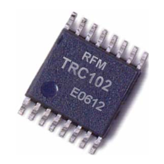
- Page 2 RF transceiver. It is an ideal fit for low cost, high volume, two way short-range wireless applications for use in the unlicensed 400-1000 MHz frequency bands. The TRC102 is FCC & ETSI certifiable and improves upon the TRC101 with improved phase noise and is capable of higher output power.
-
Page 3: Table Of Contents
Table of Contents Table of Contents........................1 1.0 TRC102 Pin Configuration ....................2 1.1 Pin Description ........................3 2.0 Functional Description ......................4 2.1 TRC102 Applications ......................4 RF Transmitter Matching....................4 Antenna Design Considerations..................5 PCB Layout Considerations ....................5 3.0 TRC102 Functional Characteristics ..................7 Input/Output Amplifier ......................7 Baseband Data and Filtering....................7... - Page 4 10.0 Package Information......................41 www.RFM.com Email: info@rfm.com Page 3 of 51 ©by RF Monolithics, Inc. TRC102 - 4/8/08...
-
Page 5: Pin Description
(5) to toggle, signaling an interrupt to an external processor. Reading the first four (4) bits of the status register tells the source of the interrupt. This pin may be used www.RFM.com Email: info@rfm.com Page 4 of 51 ©by RF Monolithics, Inc. TRC102 - 4/8/08... - Page 6 Valid Data Detector Output– This pin may be configured to indicate Valid Data when the synchronous pattern recognition circuit indicates potentially real incoming data. www.RFM.com Email: info@rfm.com Page 5 of 51 ©by RF Monolithics, Inc. TRC102 - 4/8/08...
-
Page 7: Functional Description
2. Functional Description The TRC102 is a low power, frequency agile, zero-IF, multi-channel FSK transceiver for use in the 433, 868, and 916 MHz bands. All RF and baseband functions are completely integrated requiring only a single 10MHz crystal as a reference source and an external low-cost processor. Functions include: PLL synthesizer •... -
Page 8: Antenna Design Considerations
22nH Antenna Design Considerations The TRC102 is designed to drive a differential output such as a Dipole antenna or a Loop. The loop antenna is ideally suited for applications where compact size is required. The dipole is typically not an attractive option for compact designs due to its inherent size at resonance and distance needed away from a ground plane to be an efficient antenna. - Page 9 Assembly View Top Side Bottom Side www.RFM.com Email: info@rfm.com Page 8 of 51 ©by RF Monolithics, Inc. TRC102 - 4/8/08...
-
Page 10: Trc102 Functional Characteristics
3. TRC102 Functional Characteristics F S K S DI S DO A S K S CK 0/90 DE MOD RS S I CONT ROL nIRQ RF _P T X /RX LOGIC DA T A / nF S E L RF _N... -
Page 11: Transmit Register
10 MHz reference xtal. The receive FIFO may also be configured to fill only when valid data has been identified. The TRC102 has a synchronous pattern detector that watches incoming data for a particular pattern. When it sees this pattern it begins to store any data that follows. -
Page 12: Programmable Synch Byte
Programmable Synch Byte The TRC102 may be configured to use a synch character to signal valid incoming data. This character is divided into two bytes, SB1 and SB0. SB1 is fixed to 2Dh and is not programmable. SB0 is user configurable. -
Page 13: Data Quality Detector (Dqd)
Data Quality Detector (DQD) The DQD is a unique function of the TRC102. The DQD circuit looks at the prefiltered incoming data and counts the “spikes” of noise for a predetermined period of time to get an idea of the quality of the link. -
Page 14: Ook/Ask Signaling
RSSI output. Typically, Automatic Gain Control (AGC) is used to reduce the input signal level upon saturation of the RSSI in the presence of strong or near-field ASK signals. The TRC102 does not have an AGC option, however, the input LNA gain is programmable. The output RSSI signal level may be sampled upon enabling of the receiver to test if the signal level is in saturation. -
Page 15: Low Battery Detector
50mV of hysteresis built in. SPI Interface The TRC102 is equipped with a standard SPI bus that is compatible to almost all SPI devices . All functions and status of the chip are accessible through the SPI bus. Typical SPI devices are configured for byte write operations. - Page 16 Figure 3. SPI Interface Timing www.RFM.com Email: info@rfm.com Page 15 of 51 ©by RF Monolithics, Inc. TRC102 - 4/8/08...
-
Page 17: Control And Configuration Registers
MUL1 MUL0 E196h PERIOD DUTY CYCLE DCEN C80Eh BATT DETECT CLK2 CLK1 CLK0 LBD4 LBD3 LBD2 LBD1 LBD0 C000h PLL CONFIG BUF1 BUF0 DITH PLLBW CC67h www.RFM.com Email: info@rfm.com Page 16 of 51 ©by RF Monolithics, Inc. TRC102 - 4/8/08... -
Page 18: Status Register
To read the status register, initiate a command beginning with a ‘0’ and read the remaining bits on the SDO line. All other commands begin with a ‘1’ so the TRC102 recognizes a command vs. status. See figure 4 for timing reference. - Page 19 Figure 4. Status Read Timing www.RFM.com Email: info@rfm.com Page 18 of 51 ©by RF Monolithics, Inc. TRC102 - 4/8/08...
-
Page 20: Configuration Register [Por=8008H]
PCB layout. See Table 4 below for load capacitance configuration. TABLE 4. Crystal Load CAP3 CAP2 CAP1 CAP0 Capacitance 10.5 11.5 12.5 13.5 14.5 15.5 www.RFM.com Email: info@rfm.com Page 19 of 51 ©by RF Monolithics, Inc. TRC102 - 4/8/08... - Page 21 Bit [7..6] – Mode Selection: These bits select Automatic or Manual operation. When set to Manual operation, the TRC102 will take a sample when a strobe signal (See Bit [3]) is written to the register. There are four modes of operation. See Table 5 below for configuration.
- Page 22 PLL that tunes the desired carrier frequency. Bit [0] – Offset Frequency Enable: This bit, when set, enables the TRC102 to calculate the offset frequency by the sample taken from the Automatic Frequency Adjustment circuit.
- Page 23 Max to -21dB in -3dB steps. See Table 8 below for Output Power settings. TABLE 8. Output Power (Relative) PWR2 PWR1 PWR0 -3dB -6dB -9dB -12dB -15dB -18dB -21dB www.RFM.com Email: info@rfm.com Page 22 of 51 ©by RF Monolithics, Inc. TRC102 - 4/8/08...
- Page 24 Email: info@rfm.com Page 23 of 51 ©by RF Monolithics, Inc. TRC102 - 4/8/08...
- Page 25 The SDO pin (4) may be used as a “Transmit Register Empty” flag to write the next byte. COMMAND DATA BYTE 1 DATA BYTE 2 DATA BYTE 3 Figure 6. Sequential Byte Write Timing www.RFM.com Email: info@rfm.com Page 24 of 51 ©by RF Monolithics, Inc. TRC102 - 4/8/08...
- Page 26 = 10 * B1 * (B0 + f /4000) MHz where f = decimal value of Freq[11..0] = 96<f <3903. TABLE 9. Range 433 MHz 868 MHz 916 MHz www.RFM.com Email: info@rfm.com Page 25 of 51 ©by RF Monolithics, Inc. TRC102 - 4/8/08...
Need help?
Do you have a question about the TRC102 and is the answer not in the manual?
Questions and answers