Table of Contents
Advertisement
Quick Links
MRZG2LSEVK Hardware Manual
MRZG2LSEVK Hardware Manual
Version:
1.0
Created on:
Jan 24, 2024
Created by:
ARIES Embedded GmbH
© ARIES Embedded GmbH. The information contained in this document is strictly confiden-
tial. This document may not be copied, reproduced, translated, changed or distributed
without the written approval of ARIES Embedded GmbH
Page 1 of 48
Advertisement
Table of Contents

Related Manuals for Aries Embedded MRZG2LSEVK


Summary of Contents for Aries Embedded MRZG2LSEVK
- Page 1 Jan 24, 2024 Created by: ARIES Embedded GmbH © ARIES Embedded GmbH. The information contained in this document is strictly confiden- tial. This document may not be copied, reproduced, translated, changed or distributed without the written approval of ARIES Embedded GmbH...
-
Page 2: Table Of Contents
..........2 Overview 2.1 MRZG2LSEVK - Evaluation Kit for MRZG2LS ...... - Page 3 MRZG2LSEVK Hardware Manual 3.12.2 Display Port Connector J7 ....... . .
-
Page 4: About This Manual
ARIES Embedded. ARIES Embedded explicitly reserves the rights to change or add to the contents of this Preliminary User’s Manual or parts of it without notification. -
Page 5: Registered Trademarks
The contents of this document may be subject of intellectual property rights (including but not limited to copyright, trademark, or patent rights). Any such rights that are not expressly licensed or already owned by a third party are reserved by ARIES Embedded GmbH. 1.5 Care and Maintenance •... -
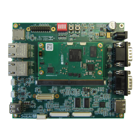
Page 6: Overview
The MRZG2LSEVK baseboard supports a quick start-up of new projects, using the MRZG2LS or MRZV2LS SMARC SoMs by ARIES Embedded. The baseboard can be used for getting in touch and first experience with the new CPU architecture, can be used as a reference platform to develop and try out software as well as it can be used to easily implement prototype setups. -
Page 7: Feature Set
MRZG2LSEVK Hardware Manual 2.2 Feature Set • MRZG2LS System on Module – Single or Dual Cortex-A55, up to 1.2GHz – 512MB – 4GB DDR4 RAM – SPI NOR – 4GB-64GB eMMC NAND Flash – compliant to the SGET SMARC 2.1 standard •... -
Page 8: Order Codes
MRZG2LSEVK Hardware Manual 2.3 Order Codes The MRZG2LSEVK is available in the following standard configurations: MRZG2LSEVK-AAB • MRZG2LS-AAB SoM featuring – Renesas RZ/G2L R9A07G044L23GBG#BC0 – 1GB DDR4 RAM – 4GB eMMC – 128MBit SPI-NOR – 2x KSZ9131 PHY 10/100/1000MBit – -25°. . . +85°C •... -
Page 9: Block Diagram
MRZG2LSEVK Hardware Manual 2.4 Block Diagram The following block diagram shows the MRZG2LSEVK with a mounted MRZG2LS SoM. Chapter 2. Overview Page 9 of 48... -
Page 10: Part Overview
MRZG2LSEVK Hardware Manual 2.5 Part Overview A more detailed and searchable document on the parts overview can be made available on request under email sales@aries-embedded.de. Chapter 2. Overview Page 10 of 48... -
Page 11: Handling Recommendations
MRZG2LSEVK Hardware Manual 2.6 Handling Recommendations To avoid mechanical damage to the components populated on MRZG2LS and MRZG2LSEVK it is strongly recommended not to apply mechanical force on the Ball Grid Array (BGA) components. Chapter 2. Overview Page 11 of 48... -
Page 12: Resources
3.1 Connector J1 - 314 Pins Edge Connector 3.1.1 Connector Part Number The MRZG2LSEVK is equipped with a 314 pins edge connector. The following connector is used on the MRZG2LSEVK and can be delivered by ARIES Embedded in mass production quantities:... -
Page 13: Pin Numbering
MRZG2LSEVK Hardware Manual 3.1.3 Pin Numbering Chapter 3. Resources Page 13 of 48... -
Page 14: Pin Out
MRZG2LSEVK Hardware Manual 3.1.4 Pin Out The following pin out table shows the connections on the MRZG2LS or MRZV2LS CPU SoM that is inserted into connector J1. 3.1.4.1 Top Side Connector/Pin Function Device/ Pin Remarks SMB_ALERT# n.c. CSI1_CK+ MPU AG13... - Page 15 MRZG2LSEVK Hardware Manual Table 1 – continued from previous page Connector/Pin Function Device/ Pin Remarks SPI0_CS0# n.c. SPI0_CK n.c. SPI0_DIN n.c. SPI0_DO n.c. SATA_TX+ n.c. SATA_TX- n.c. SATA_RX+ n.c. SATA_RX- n.c. SPI1_CS0# MPU B19 SPI1_CS1# n.c. SPI1_CK MPU A19 SPI1_DIN...
- Page 16 MRZG2LSEVK Hardware Manual Table 1 – continued from previous page Connector/Pin Function Device/ Pin Remarks HDMI_D2+ n.c. HDMI_D2- n.c. HDMI_D1+ n.c. HDMI_D1- n.c. HDMI_D0+ n.c. HDMI_D0- n.c. P100 P101 HDMI_CK+ n.c. P102 HDMI_CK- n.c. P103 P104 HDMI_HPD n.c. P105 HDMI_CTRL_CK n.c.
- Page 17 MRZG2LSEVK Hardware Manual Table 1 – continued from previous page Connector/Pin Function Device/ Pin Remarks P138 SER2_RTS# n.c. P139 SER2_CTS# n.c. P140 SER3TX MPU A15 P141 SER3_RX MPU B15 P142 P143 CAN0_TX MPU AH22 P144 CAN0_RX MPU AG22 P145 CAN1_TX...
-
Page 18: Bottom Side
MRZG2LSEVK Hardware Manual 3.1.4.2 Bottom Side Connector/Pin Function Device/ Pin Remarks I2C_CAM1_CK MPU B24 I2C_CAM1_DAT MPU A25 RSVD n.c. I2C_CAM0_CK n.c. CAM_MCK n.c. I2C_CAM_DAT n.c. CSI0_CK+ n.c. CSI0_CK- n.c. CSI0_RX0+ n.c. CSI0_RX0- n.c. CSI0_RX1+ n.c. CSI0_RX1- n.c. GBE1_MDIO+ PHY2 2... - Page 19 MRZG2LSEVK Hardware Manual Table 2 – continued from previous page Connector/Pin Function Device/ Pin Remarks I2C_GP_CK MPU D3 I2C_GP_DAT MPU C2 I2S2_LRCK MPU A10 I2S2_SDOUT MPU C12 I2S2_SDIN MPU D13 I2S2_CK MPU B10 SATA_ACT# n.c. USB5_EN_OC# n.c. QSPI_IO_2 n.c. QSPI_IO_3 n.c.
- Page 20 MRZG2LSEVK Hardware Manual Table 2 – continued from previous page Connector/Pin Function Device/ Pin Remarks DP0_LANE1- n.c. HDMI_D0+ n.c. HDMI_D0- n.c. S100 DP0_LANE2- n.c. S101 S102 HDMI_CK- n.c. S103 DP0_LANE3- n.c. S104 HDMI_HPD n.c. S105 HDMI_CTRL_CK n.c. S106 HDMI_CTRL_DA n.c.
-
Page 21: Ethernet
MRZG2LSEVK Hardware Manual Table 2 – continued from previous page Connector/Pin Function Device/ Pin Remarks S146 PCIE_WAKE# n.c. S147 VDD_RTC S148 LID# n.c. S149 SLEEP# n.c. S150 VIN_PWR_BAD# PMIC 47 S151 CHARGING# n.c. S152 CHARGER_PRSNT# n.c. S153 CARRIER_STBY# PMIC 56... -
Page 22: Usb
MRZG2LSEVK Hardware Manual 3.3 USB 3.3.1 USB0 (OTG) The USB0 interface is available as USB2.0 OTG interface on connector J4 and connected to the following curcuitry: The USB0 interface makes use of the following signals: Signal J1 Pin USB0_VBUS_DET USB0_EN_OC#... -
Page 23: Usb1 (Host)
MRZG2LSEVK Hardware Manual 3.3.2 USB1 (Host) The USB1 interface is available as USB2.0 host interface on connector J6 and connected to the following curcuitry: The USB0 interface makes use of the following signals: Signal J1 Pin USB1_EN_OC# USB1_N USB1_P 3.4 UART UART0 and UART3 of the MRZG2LS are routed to a CP2105 device. -
Page 24: Jtag
MRZG2LSEVK Hardware Manual 3.5 JTAG The JTAG interface of the MRZG2LS is available on a FPC-connector on the SoM itself and not routed to the baseboard, accordingly. For more information please refer to the MRZG2LS hardware manual. 3.6 CAN The CAN0 and CAN1 interfaces of are available on DUB9 connectors P5 and P6. -
Page 25: Can1
MRZG2LSEVK Hardware Manual The 60 Ohm termination of the CAN0 interface can be activated by closing jumper JP1. 3.6.2 CAN1 SoM Signal MCP2562-E P6 Pin Remark signal CAN1_TX P145 n.c. n.c. n.c. n.c. n.c. CAN1_RX P146 n.c. n.c. n.c. 1.8V n.c. -
Page 26: Sd-Card
MRZG2LSEVK Hardware Manual 3.7 SD-card The MSRZG2LSEVK supports a µSD-card slot on connector J2. The interface is connected as follows: SoM Signal J1 Pin Remark SDIO_CK SDIO_CMD pullup 10k SDIO_CD SDIO_WP SDIO_D0 pullup 10k SDIO_D1 pullup 10k SDIO_D2 pullup 10k... -
Page 27: Miscellaneous Signals
MRZG2LSEVK Hardware Manual 3.8 Miscellaneous Signals Connector P1 hosts various signals on a 2.54” pin header: P1 Pin Signal Name J1 Pin Remark n.a. n.c. VCC 1.8V n.a. n.c. VCC3V3 P126 SET_OUT# I2C_GP_CK SER1_TX P134 33R serial I2C_GP_DAT SER1_RX P135... -
Page 28: Power Button
MRZG2LSEVK Hardware Manual 3.10 Power Button Switch P3 acts a power button to start an inactive CPU SoM, depending on the configuration of the CPU SoM. Closing P3 pulls signal POWER_BTN# contact P128 of the 314 pins edge connector P1 to GND. -
Page 29: Dsi Display Subsystem
MRZG2LSEVK Hardware Manual 3.12 DSI Display Subsystem 3.12.1 TC9595 DSI Converter U8 The DSI/DPI to DisplayPort converter (TC9595XBG) is a bridge device that enables video streaming from a Host (application or baseband processor) over MIPI ® DSI or DPI link to drive DisplayPort display panels. - Page 30 MRZG2LSEVK Hardware Manual On the MRZG2LSEVK the U8 DSI converter is connected as follows: Chapter 3. Resources Page 30 of 48...
- Page 31 MRZG2LSEVK Hardware Manual Signals direction from the CPU Signal/P1 Pin TC9595BGX Device/Pin Remark Signal DSI0_CLK_N/S135 DSI0_CLK_P/S134 DSI0_D0_N/S126 DSI0_D0_P/S125 DSI0_D1_N/S129 DSI0_D1_P/S128 DSI0_D2_N/S132 DSI0_D2_P/S131 DSI0_D3_N/S138 DSI0_D3_P/S137 Y1/3 26MHz ref.clock RESET_OUT#/P126 GPIO2/DSI_INT pull down 10k I2S0_LRCLK/S39 I2S0_CK/S42 AUDIO_MCK/S38 I2S0_SDOUT/S40 I2C_LCD_DAT/S140 J9/4 via voltage...
- Page 32 MRZG2LSEVK Hardware Manual Signals direction to the display interface Signal/P1 Pin TC9595BGX Device/Pin Remark Signal DPLNP0/J3 J7/1 DPLNM0/K3 J7/3 DPLNP1/J6 J7/4 DPLNM1/K6 J7/6 DPAUXP/J8 J7/15 DPAUXM/K6 J7/17 DPID0/A4 J8/21 RGB B DPID1/B5 J8/22 RGB B DPID2/B6 J8/23 RGB B DPID3/A7...
-
Page 33: Display Port Connector J7
MRZG2LSEVK Hardware Manual 3.12.2 Display Port Connector J7 The MRZG2LSEVK hosts a Display Port interface on connector J7 type Molex 0472720024. J7 is connected to the TC9595 DSI Converter U8. 3.12.3 RGB-Display Connector J8 TC9595BGX U8 Signal J8 Pin Remark... -
Page 34: Touch Screen Connector J9
MRZG2LSEVK Hardware Manual 3.13 Touch Screen Connector J9 TC9595BGX U8 Signal J9 Pin Remark I2C_SCL/A10 I2C_SAD/A9 GPIO13/CTP_INT# /P1 S123 RESET_OUT#/P1 P126 Chapter 3. Resources Page 34 of 48... -
Page 35: Lvds-Display Connector J10
MRZG2LSEVK Hardware Manual 3.14 LVDS-Display Connector J10 The MRZG2LSEVK hosts a LVDS-display interface to be used with SMARC SoMs other than the MRZG2LS. The interface is available on connector J10 and provides the following signals: J10 Pin Connector P1 Contact/ Signal... -
Page 36: Camera Interface P7
MRZG2LSEVK Hardware Manual 3.15 Camera Interface P7 The MRZG2LSEVK provides the MIPI-CSI2 camera interface of the RZ/G2L CPU on connector P7, type Amphenol 61083-044402LF: P7 Pin Connector P1 Contact/ Signal Remarks CAM_MCK/S6 CSI1_CK_P/P3 n.c. CSI1_CK_N/P4 n.c. CSI1_RX0_P/P7 n.c. CSI1_RX0_N/P8 n.c. -
Page 37: Schematics
MRZG2LSEVK Hardware Manual CHAPTER FOUR SCHEMATICS A more detailed and searchable document on the parts overview can be made available on request under email sales@aries-embedded.de. Chapter 4. Schematics Page 37 of 48... - Page 38 MRZG2LSEVK Hardware Manual Chapter 4. Schematics Page 38 of 48...
- Page 39 MRZG2LSEVK Hardware Manual Chapter 4. Schematics Page 39 of 48...
- Page 40 MRZG2LSEVK Hardware Manual Chapter 4. Schematics Page 40 of 48...
- Page 41 MRZG2LSEVK Hardware Manual Chapter 4. Schematics Page 41 of 48...
- Page 42 MRZG2LSEVK Hardware Manual Chapter 4. Schematics Page 42 of 48...
- Page 43 MRZG2LSEVK Hardware Manual Chapter 4. Schematics Page 43 of 48...
- Page 44 MRZG2LSEVK Hardware Manual Chapter 4. Schematics Page 44 of 48...
- Page 45 MRZG2LSEVK Hardware Manual Chapter 4. Schematics Page 45 of 48...
- Page 46 MRZG2LSEVK Hardware Manual Chapter 4. Schematics Page 46 of 48...
- Page 47 MRZG2LSEVK Hardware Manual Chapter 4. Schematics Page 47 of 48...
-
Page 48: Contents
MRZG2LSEVK Hardware Manual Chapter 4. Schematics Page 48 of 48...
Need help?
Do you have a question about the MRZG2LSEVK and is the answer not in the manual?
Questions and answers