Table of Contents
Advertisement
Quick Links
Please refer to the original service manual for:
Speaker system SB-CT500EG-K, Order No. PSG1511002CE (For SU-C500EB/EG/GN/PP only)
TABLE OF CONTENTS
1 Safety Precautions----------------------------------------------- 3
1.1. General Guidelines---------------------------------------- 3
1.2. Before Repair and Adjustment ------------------------- 4
1.3. Protection Circuitry ---------------------------------------- 4
1.4. Caution For AC Cord (For EB) ------------------------- 5
Model No.
Product Color: (S)...Silver Type
PAGE
1.5. Safety Parts Information----------------------------------6
2 Warning --------------------------------------------------------------7
2.1. Prevention of Electrostatic Discharge (ESD)
to Electrostatically Sensitive (ES) Devices ----------7
2.2. Precaution of Laser Diode -------------------------------7
© Panasonic Corporation 2015. All rights reserved.
Unauthorized copying and distribution is a violation
of law.
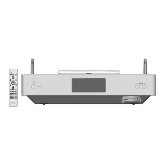
CD Stereo System
SU-C500EB
SU-C500EG
SU-C500GN
SU-C500PP
SU-C550EB
SU-C550EG
SC-C500EB
SC-C500EG
SC-C500GN
SC-C500PP
PSG1511001CE
A6
PAGE
Advertisement
Table of Contents


Need help?
Do you have a question about the SU-C500EB and is the answer not in the manual?
Questions and answers