Table of Contents
Advertisement
Quick Links
Service
Manual
5 CHANNEL POWER AMPLIFIER
GM-D515
For details, refer to "Important symbols for good services".
PIONEER CORPORATION
PIONEER ELECTRONICS (USA) INC.
PIONEER EUROPE NV
Haven 1087 Keetberglaan 1, 9120 Melsele, Belgium
PIONEER ELECTRONICS ASIACENTRE PTE.LTD. 253 Alexandra Road, #04-01, Singapore 159936
C PIONEER CORPORATION 2004
GM-D515/X1H/EW
4-1, Meguro 1-Chome, Meguro-ku, Tokyo 153-8654, Japan
P.O.Box 1760, Long Beach, CA 90801-1760 U.S.A.
/X1H/EW
K-ZZB. SEPT. 2004 Printed in Japan
ORDER NO.
CRT3309
Advertisement
Table of Contents

Related Manuals for Pioneer GM-D515/X1H


Summary of Contents for Pioneer GM-D515/X1H
- Page 1 PIONEER ELECTRONICS (USA) INC. P.O.Box 1760, Long Beach, CA 90801-1760 U.S.A. PIONEER EUROPE NV Haven 1087 Keetberglaan 1, 9120 Melsele, Belgium PIONEER ELECTRONICS ASIACENTRE PTE.LTD. 253 Alexandra Road, #04-01, Singapore 159936 C PIONEER CORPORATION 2004 K-ZZB. SEPT. 2004 Printed in Japan...
-
Page 2: Safety Information
Health & Safety Code Section 25249.6 - Proposition 65 - Service Precaution You should conform to the regulations governing the product (safety, radio and noise, and other regulations), and should keep the safety during servicing by following the safety instructions described in this manual. GM-D515/X1H/EW... - Page 3 To protect products from damages or failures during transit, the shipping mode should be set or the shipping screws should be installed before shipment. Please be sure to follow this method especially if it is specified in this manual. GM-D515/X1H/EW...
-
Page 4: Table Of Contents
7. GENERAL INFORMATION........28 2.1 PACKING..............6 7.1 DIAGNOSIS ............28 2.2 EXTERIOR ............8 7.1.1 DISASSEMBLY.........28 3. SCHEMATIC DIAGRAM...........10 7.1.2 ..29 CONNECTOR FUNCTION DESCRIPTION 3.1 SCHEMATIC DIAGRAM (GUIDE PAGE) ...10 8. OPERATIONS ............30 4. PCB CONNECTION DIAGRAM........18 4.1 AMP UNIT............18 4.2 NETWORK UNIT..........22 GM-D515/X1H/EW... -
Page 5: Specifications
• Specifications and the design are subject to possible modification without notice due to improvements. *Average current drawn • The average current drawn is nearly the maximum current drawn by this unit when an audio signal is input. Use this value when working out total current drawn by multiple power amplifiers. GM-D515/X1H/EW... -
Page 6: Exploded Views And Parts List
2. EXPLODED VIEWS AND PARTS LIST 2.1 PACKING GM-D515/X1H/EW... - Page 7 7-2 Warranty Card HRY1157 8 Carton HHG0450 9 Contain Box HHL0450 10 Core HTX0003 11 Lock Tie HNV0025 12 Caution Card HRP1296 13 Polyethylene Bag HEG0025 - Owner's Manual Part No. Language HRD0276 English, Spanish, German, French, Italian, Dutch GM-D515/X1H/EW...
-
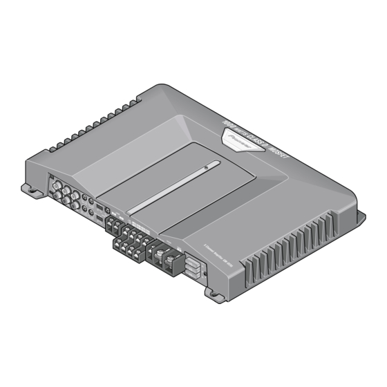
Page 8: Exterior
2.2 EXTERIOR 38(2/2) 46(1/2) 38 ( 1/2 ) 46(2/2) 54 54 GM-D515/X1H/EW... - Page 9 35 Holder HNC0143 36 Holder HNC0144 37 Buss Bar HNC0212 38 Insulator HNM0125 39 Insulator HNM8405 40 Bar HNR0124 41 Heat Sink HNR0266 42 Heat Sink HNR0267 43 Heat Sink HNR1720 44 Beads Core HTF0001 45 Beads Core HTF0003 GM-D515/X1H/EW...
-
Page 10: Schematic Diagram
No differentiation is made between chip capacitors and ← 0.022 R022 discrete capacitors. The > mark found on some component parts indicates the importance of the safety factor of the part. Therefore, when replacing, be sure to use parts of identical designation. GM-D515/X1H/EW... - Page 11 AMP UNIT POWER AMP POWER AMP POWER AMP POWER AMP OVER VOLTAGE PROTECTOR NETWORK UNIT > Consists of NETWORK PCB > CONNECTOR PCB > CONNECTOR GM-D515/X1H/EW...
- Page 12 A-a B GM-D515/X1H/EW...
- Page 13 GM-D515/X1H/EW...
- Page 14 GM-D515/X1H/EW...
- Page 15 GM-D515/X1H/EW...
- Page 16 1 Power supply switching waveform measured at TP638 and TP639. 2 BRem TP624, Stand-by line TP253, Mute line TP254 timing diagram. 3 Class D switching audio waveform at no signal {TP413 and / or TP414} same waveform on both test points. GM-D515/X1H/EW...
- Page 17 GM-D515/X1H/EW...
-
Page 18: Pcb Connection Diagram
For further information for respective destinations, be sure to check with the schematic dia- gram. 2.Viewpoint of PCB diagrams Capacitor Connector SIDE A SIDE B P.C.Board Chip Part CN102 SUB FREQ B FREQ B GAIN B HPF GM-D515/X1H/EW... - Page 19 SIDE A FUSE FUSE CN703 CN701 CN702 FUSE GM-D515/X1H/EW...
- Page 20 AMP UNIT GM-D515/X1H/EW...
- Page 21 SIDE B GM-D515/X1H/EW...
-
Page 22: Network Unit
4.2 NETWORK UNIT NETWORK PCB SIDE A SIDE B NETWORK PCB CN103 CONNECTOR PCB CONNECTOR PCB SIDE A SIDE B CN601 CN601 CN601 GM-D515/X1H/EW... -
Page 23: Electrical Parts List
2SA1037K Ferri-Inductor CTF1007 Transistor 2SA1037K Ferri-Inductor CTF1007 Transistor 2SC2412K Ferri-Inductor CTF1007 Transistor 2SC2412K Transformer HTT0036 Transistor 2SD2395 Thermistor HCX0002 Transistor 2SB1566 Thermistor HCX0002 Transistor DTA114EK Thermistor HCX0003 Transistor DTC114TK Thermistor HCX0003 Transistor 2SC2412K Thermistor HCX0003 Transistor DTC114TK Thermistor HCX0002 GM-D515/X1H/EW... - Page 24 RS1/16S103J RS1/16S152J RS1/16S103J RS1/16S152J RS1/16S222J RS1/16S152J RS1/16S222J RS1/16S152J RD1/4PU202J RD1/4PU102J RD1/4PU102J RD1/4PU202J RD1/4PU102J RD1/4PU102J RD1/4PU102J RD1/4PU473J RD1/4PU512J RD1/4PU103J RD1/4PU103J RD1/4PU512J RS1/16S474J RD1/4PU222J RS1/16S474J RD1/4PU472J RS1/16S272J RD1/4PU472J RS1/16S272J RD1/4PU472J RD1/4PU472J RS1/16S101J RS1/16S101J RD1/4PU103J RN1/16SE4301D RD1/4PU472J RN1/16SE3901D RD1/4PU101J RD1/4PU560J RD1/4PU221J RS1/16S102J GM-D515/X1H/EW...
- Page 25 CFTNA184J50 RS1/2PMF100J CFTNA184J50 RS1/2PMF100J CFTNA224J50 RS1/16S272J CFTNA224J50 RS1/16S242J CEAT100M16 RS1/16S471J CEAT1R0M50 RS1/16S471J CEAT1R0M50 RS1/16S223J CEAT100M16 RS1/16S223J CCSRCH121J50 RN1/10SE1002D CCSRCH121J50 RN1/10SE1002D CCSRCH470J50 RN1/10SE1002D CCSRCH470J50 RN1/10SE1002D CEAT100M50 RN1/10SE1002D CEAT100M50 RN1/10SE1002D CEAT100M50 RN1/10SE1002D CEAT100M50 RN1/10SE1002D CKSRYB222K50 RS1/16S562J CKSRYB222K50 RS1/16S562J CKSRYB102K50 RS1/16S562J CKSRYB102K50 GM-D515/X1H/EW...
- Page 26 CFTNA103J50 CFTLA105J50 CFTNA103J50 CKSRYB471K50 CFTNA103J50 CKSRYB471K50 CQMA102J50 CKSRYB471K50 CQMA102J50 CKSRYB471K50 CQMA102J50 CFTNA333J50 CQMA102J50 CFTNA333J50 CQMA102J50 CQMA102J50 3300µF/16V HCH0006 CQMA102J50 3300µF/16V HCH0006 CKSRYB103K50 3300µF/16V HCH0006 CKSRYB103K50 3300µF/16V HCH0006 CKSRYB103K50 3300µF/16V HCH0006 CKSRYB103K50 3300µF/16V HCH0006 CEHAT220M50 3300µF/16V HCH0006 CEHAT220M50 3300µF/16V HCH0006 GM-D515/X1H/EW...
-
Page 27: Adjustment
CFTNA224J50 CCSRCH470J50 CFTNA224J50 CCSRCH470J50 CCSRCH470J50 CCSRCH470J50 CCSRCH470J50 CCSRCH470J50 CKSRYB103K50 CKSRYB471K50 CKSRYB103K50 CKSRYB471K50 CKSRYB103K50 CEAT100M50 CKSRYB103K50 CEAT100M50 CKSRYB103K50 CKSRYB472K50 CKSRYB103K50 CKSRYB472K50 CKCYB472K50 CCSRCH470J50 CCSRCH470J50 CCSRCH470J50 CCSRCH470J50 220µF/10V HCH0012 6. ADJUSTMENT There is no information to be shown in this chapter. GM-D515/X1H/EW... -
Page 28: General Information
7.1.1 DISASSEMBLY Removing the Case (Fig.1) Remove the three screws. Remove the nine screws and then remove the Case. Fig.1 Case Removing the Amp Unit (Fig.2) Remove the nine screws and then remove the Amp Unit. Amp Unit Fig.2 GM-D515/X1H/EW... -
Page 29: Connector Function Description
7.1.2 CONNECTOR FUNCTION DESCRIPTION GM-D515/X1H/EW... -
Page 30: Operations
8. OPERATIONS GM-D515/X1H/EW...
Need help?
Do you have a question about the GM-D515/X1H and is the answer not in the manual?
Questions and answers