
Related Manuals for Picotest J2103A


Summary of Contents for Picotest J2103A
- Page 1 J2103A Power Stage Isolator Operation Manual Dated: 06/07/2023 Copyright 2023 Picotest Version 1.1...
-
Page 2: Table Of Contents
2. J2103A Package Contents ....................... 3 3. Side Panel Configuration 1 ......................5 4. Side Panel Configuration 2 ......................6 5. J2103A Operation Steps ........................8 6. The OSC signal level for J2103A ....................9 7. Specifications ..........................10 8. Inspection ............................10... -
Page 3: Introduction To J2103A
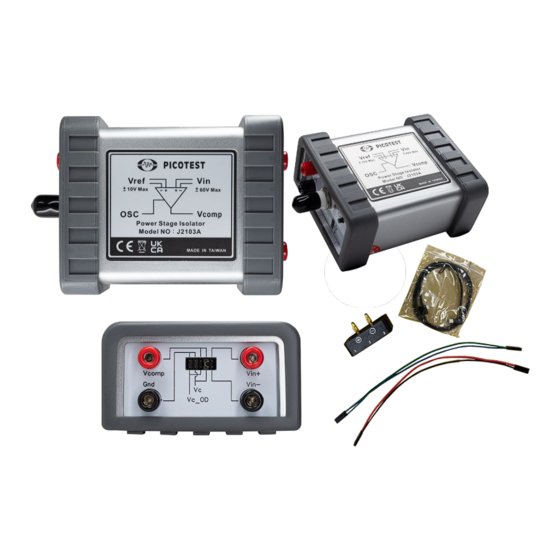
However, the whole process was very time-consuming and cumbersome. J2103A Power Stage Isolator is a device that replaces feedback control circuits to control the power output circuit (Power stage). The advantage of using J2103A before designing the feedback control circuit is that we can perform frequency response measurements on the power stage output circuit and design the feedback control circuit based on the actual measurement results. - Page 4 J2103A Power Stage Isolator Figure 1 J2103A Product Contents *Note 1: For battery transportation, please refer to the lithium battery product transportation regulations in “The shipping resulations for lithium batteries.pdf”. *Note 2: For more information on the banana plug to USB converter, please refer to the PWR-OPT03...
-
Page 5: Side Panel Configuration 1
The configuration diagram of panel 1 for J2103A is shown in Figure 2. Figure 2 J2103A Panel Configuration I According to Figure 2, J2103A provides two types of input/output ports: Banana jacks and Dupont connectors: a. You can select Vcomp output using the Dupont terminals. By connecting pin 5 to pin 6 with a jumper cap, you can set Vcomp to open drain output. -
Page 6: Side Panel Configuration 2
J2103A Power Stage Isolator 4. Side Panel Configuration 2 The configuration diagram of panel 2 for J2103A is shown in Figure 3. Figure 3 J2103A Panel Configuration 2 Figure 3-1 Power Indicator Lights Figure 3-1 shows the Power indicator lights: a. - Page 7 Figure 3-3 USB Type-C Charging Port The USB Type-C charging port shown on Figure 3-3 is for charging only. When J2103A is being charged, the power switch will automatically turn off and cannot be operated. A 5V, 15W USB charger adapter...
-
Page 8: J2103A Operation Steps
J2103A Power Stage Isolator 5. J2103A Operation Steps Figure 4 is the circuit diagram of J2103A. Plesase operate according to the following instructions. a. Turn off the DC power supplies A, B, and J2103A power. b. Configure the DUT to be controlled by J2103A. -
Page 9: The Osc Signal Level For J2103A
There is an OSC to Vcomp port signal attenuation ratio of 20dB. The J2103A operates with a single power supply, and the Vcomp output range is 0~10V. Therefore, the strength of the OSC signal, represented by Vosc/10, must be lower than the DC bias value of Vcomp under no clamp condition. -
Page 10: Specifications
+26dBm, and there is a 20dB attenuation from OSC to Vcomp. The bandwidth is greater than 1MHz. d. Four LTO batteries are connected in series to power the J2103A. They can be fully charged in about 30 minutes and can work continuously for more than 8 hours with Vcomp=10V at no-load and the OSC port not connected. - Page 11 Figure 7 Frequency response of Vin to Vcomp J2103A Power Stage Isolator Figure 8 Frequency response of OSC to Vcomp...
Need help?
Do you have a question about the J2103A and is the answer not in the manual?
Questions and answers