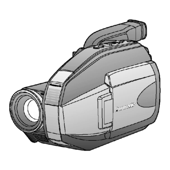
Panasonic PV-L452 Service Manual
Compact vhs camcorder
Hide thumbs
Also See for PV-L452:
- Operating instructions manual (60 pages) ,
- Operating instructions manual (60 pages)

Related Manuals for Panasonic PV-L452


Summary of Contents for Panasonic PV-L452
- Page 1 ORDER NO. MKE0112200C1 B15 (U.S.A.), B4 (PUERTO RICO) Compact VHS Camcorder PV-L452 / PV-L652 SPECIFICATIONS...
- Page 2 1. SAFETY PRECAUTIONS GENERAL GUIDELINES 1. IMPORTANT SAFETY NOTICE There are special components used in this equipment which are important for safety. These parts are marked by in the Schematic Diagrams, Circuit Board Layout, Exploded Views and Replacement Parts List. It is essential that these critical parts should be replaced with manufacturer's specified parts to prevent X-RADIATION, shock, fire, or other hazards.
- Page 3 When the exposed metallic part has a return path to the chassis, the reading should be between 1 M and 5.2 M . When the exposed metal does not have a return path to the chassis, the reading must be infinity. LEAKAGE CURRENT HOT CHECK (See Figure 1.) 1.
- Page 4 components commonly are called Electrostatically Sensitive (ES) Devices. Examples of typical ES devices are integrated circuits and some field-effect transistors and semiconductor "chip" components. The following techniques should be used to help reduce the incidence of component damage caused by electro static discharge (ESD). 1.
- Page 5 together of your clothes fabric or the lifting of your foot from a carpeted floor can generate static electricity (ESD) sufficient to damage an ES device). 3. OPERATION GUIDE 4. SERVICE NOTES (PLEASE READ) 4.1. SERVICE NOTES 4.1.1. EXTENSION CABLES FOR SERVICE NOTE: 1.
- Page 6 5. When servicing with the Main C.B.A. installed on the VCR Mechanism Chassis Ass'y (Main C.B.A. in raised position), tighten 2 Screws for stability. 6. Use a grounded ESD wrist strap while disassembling the Lens portion. 7. Use extreme care when unplugging or plugging in connectors. Fig.
- Page 7 To hold the Cassette Up Unit in the down position without it, a Lock Screw is needed. 4.1.2.1. How to install the Lock Screw: 1. If the Lock Lever, shown in gray, is set to Position "A" (No hole), change Position "A" (No hole) to Position "B" (Hole) as shown in Fig.
- Page 8 2. Install the Lock Screw in the Hole (Threaded Hole for Lock Screw access) in Position "B". 3. Hold down the Cassette Up Unit and confirm that the Cassette Up Unit will stay in the down position. Note: If the Cassette Up Unit will not stay in the down position, slide the Lock Lever to the right slightly.
- Page 9 4.1.3. SERVICE MODE SPECIFICATION (SELF-DIAGNOSTIC SYSTEM) Operation: 1. Start-up: Press and hold all of the Display, REC, and Stop buttons over 2 seconds, the unit goes into the self- diagnostic mode and main menu appears. 2. Mode Selection: Press display button to change and select self- diagnose mode.
- Page 14 If any of the following numbers appear on-screen in Photo mode, the palmcorder may need service. Do not remove the battery (if attached) and write down the displayed number.
- Page 15 Note: While battery remains, the Error No. will be displayed again when the power is switched off and on again. (Once the Battery is removed or dead, Error No. will not remain in the memory.) 4.1.4. REMOVAL/INSTALLATION OF F.P.C. FROM NON ZIF (ZERO INSERTION FORCE) CONNECTOR Removal/Installation of F.P.C.
- Page 16 3. Connect the F.P.C.s to the Non ZIF connectors, verifying the direction of F.P.C as shown. Fig. 3-2 4.1.5. METHOD FOR LOADING/UNLOADING OF MECHANISM 4.1.5.1. (Electrical Method) CAUTION: If loading does not start after DC Power Supply is applied, DO NOT continue to applying DC Power Supply.
- Page 17 It normally takes approx. 6 seconds to unload the Mechanism from fully-loaded position to EJECT position. Fig. 4-1 4.1.5.2. (Manual Method) without Cabinet Parts Turn the Gear of Reduction Gear Unit clockwise (for loading) or counterclockwise (for unloading) manually. It is necessary to rotate approx. 80 times from fully-loaded position to EJECT position. Fig.
- Page 18 continue applying DC Power Supply. Remove a jammed tape as follows: 1. Remove a Screw and remove the EVR Cover. Fig. 5-1 2. Place the unit with the Cassette Cover facing upward. 3. Connect the TP Board through the TP Board slot. 4.
- Page 19 5. Open the Cassette Cover fully. 6. Remove the tape slack by rotating the Takeup Reel Gear of the cassette tape. Fig. 5-3 7. Take out the cassette tape. 8. Connect the Power or Battery to set the Mechanism to STOP Position.
- Page 20 4.1.7.3. How to connect TP Board to Camcorder: 1. Connect the TP Board to Camcorder as shown. Fig. 6-2...
- Page 21 4.1.7.4. Signal description on TP Adjustment P.C.B. 40P (VFKW0123B) Fig. 6-3-1...
- Page 22 Fig. 6-3-2...
- Page 23 Fig. 6-3-3...
- Page 24 4.1.8. EEPROM DATA CAUTION: Be sure to save the EEPROM data using PC-EVR Adjustment Program before service and adjustment in order to make sure to avoid an accidental data loss, etc. as follows. Refer to "SET UP OF PC-EVR ADJUSTMENT PROGRAM"...
- Page 25 How to save the EEPROM data to your PC 1. Start up the PC-EVR Adjustment Program. 2. Select "1. Read (Save)/Write AII EEPROM datas." in Main menu, and then press "Enter" key. 3. Select "1. Save all data of EEPROM" in Read (Save)/Write All EEPROM datas menu, and then press "Enter"...
- Page 26 Fig. 7 4.1.10. HOW TO ACCESS THE MANUAL TRACKING CONTROL 4.1.11. REPLACEMENT PROCEDURE FOR LEADLESS (CHIP) COMPONENT The following procedures are recommended for the replacement of the leadless components used in this Unit. 1. Preparation for replacement A. Soldering Iron Use a pencil-type soldering iron using less than 30 watts.
- Page 27 Do not apply heat for more than 4 seconds. D. Preheating Leadless capacitor must be preheated before installation. (130 °C ~ 150 °C, for about 2 minutes.) Note: A. Leadless component must not be reused after removal. B. Excessive mechanical stress and rubbing of the component electrode must be avoided.
- Page 28 Note: Do not glue the replacement leadless component to the circuit board. 4.1.12. SPECIAL NOTE All integrated circuits and many other semiconductor devices are electrostatically sensitive and therefore require the special handlings techniques described under the "ELECTROSTATICALLY SENSITIVE (ES) DEVICES" section of this service manual. 4.1.13.
- Page 29 and Circuit Board Layout Notes, for Mark "PT." 5. DISASSEMBLY/ASSEMBLY PROCEDURES 5.1. CABINET SECTION 5.1.1. DISASSEMBLY FLOWCHART This flow chart indicates the disassembly steps of the cabinet parts and the P.C.Boards in order to gain access to item (s) to be serviced. When reassembling, perform the step (s) in the reverse order.
- Page 30 5.2.2. Inner Parts Location 5.2.2.1. TOP VIEW Fig. DM1-1...
- Page 31 5.2.2.2. BOTTOM VIEW Fig. DM1-2 5.2.3. STOP Position Confirmation Fig. DM2...
- Page 32 Perform all disassembly and alignments procedures in STOP Position except disassembly and alignment procedures which have the special Notes. 5.2.4. Cassette Up Unit Fig. DM3-1...
- Page 33 Fig. DM3-2...
- Page 34 5.2.5. Cylinder Unit Fig. DM4-1-1...
- Page 35 Fig. DM4-1-2...
- Page 36 5.2.6. Cylinder/Head Amp F.P.C., Bugle Chip Fig. DM4-2 5.2.7. P.C.B. Angle Fig. DM5...
- Page 37 5.2.8. Mechanism F.P.C Unit Fig. DM6-1...
- Page 38 Fig. DM6-2...
- Page 39 5.2.9. Tension Unit, Reel Table Unit Fig. DM7-1...
- Page 40 Fig. DM7-2...
- Page 41 5.2.10. Rev Clutch Fig. DM8...
- Page 42 5.2.11. Take Gear, Rev Brake Arm Unit Fig. DM9-1 Fig. DM9-2...
- Page 43 5.2.12. A/C Head Unit Fig. DM10...
- Page 44 5.2.13. Capstan Belt Fig. DM11...
- Page 45 5.2.14. Capstan Unit Fig. DM12...
- Page 46 5.2.15. Idle Arm Unit Fig. DM13...
- Page 47 5.2.16. Mechanism Support Angle Fig. DM14...
- Page 48 5.2.17. Reduction Gear B Fig. DM15 5.2.18. Reduction Gear A, Reduction Gear Unit Fig. DM16...
- Page 49 5.2.19. Pinch Arm Unit Fig. DM17...
- Page 50 5.2.20. Takeup Post Unit, Supply Post Unit Fig. DM18-1...
- Page 51 Fig. DM18-2...
- Page 52 5.2.21. Impedance Roller Unit, Loading Base Unit Fig. DM19-1...
- Page 53 Fig. DM19-2...
- Page 54 5.2.22. Takeup Loading Arm Unit Fig. DM20...
- Page 55 5.2.23. Supply Loading Arm Unit Fig. DM21-1...
- Page 56 Fig. DM21-2...
- Page 57 Fig. DM21-3...
- Page 58 5.2.24. Loading Motor Unit, Main Cam Unit, Pinch Toggle Fig. DM22...
- Page 59 6. ADJUSTMENT PROCEDURES 6.1. SERVICE FIXTURES & TOOLS...
- Page 60 6.2. MECHANICAL ADJUSTMENT 6.2.1. CLEANING PROCEDURE FOR THE UPPER CYLINDER UNIT 1. While slowly turning the Upper Cylinder Unit counterclockwise by hand, gently rub the Video Heads with a Head Cleaning Stick (VFK27) moistened with Isopropyl Alcohol 91 %. Fig. M1 Note: A.
- Page 61 2. Put the unit into the service mode "I. TRACKING FIX" to defeat Auto Tracking. Refer to "SERVICE MODE SPECIFICATION (SELF- DIAGNOSTIC SYSTEM)" in "SERVICE NOTES." 3. Remove the Cassette Lid Cover from the Cassette Tape or the Alignment Tape. Fig.
- Page 62 If the envelope is output poorly, much noise will appear in the picture. Then the tracking will lose precision and the playback picture will be distorted by any slight variation of the tracking control circuit. 1. Put the unit into the service mode "I. Tracking Fix" to defeat Auto Tracking.
- Page 63 Note: It will be possible to confirm step 4) after performing the following steps. A. Exit the "I. TRACKING FIX" mode, then skip the "J. PG SHIFTER" mode to enter other modes (except these 2). Or, close the service mode. B.
- Page 64 slightly and equally adjust Screw A, Screw B, and Screw C on the A /C Head Unit to achieve the sub control signal level of 500 mV±200 (Sub Control Signal level will decrease when rotating screws clockwise, and increase when rotating screws counterclockwise.) Fig.
- Page 65 5. Confirm and readjust the A/C Head height. 6. Confirm and readjust Screw C (Azimuth) on the A/C Head so that the output audio becomes is maximum. 6.2.2.1.4. A/C HEAD HORIZONTAL POSITION ADJUSTMENT Purpose: To adjust the Horizontal Position of the A/C Head. Symptom of Misadjustment: If the Horizontal Position of the A/C Head is not properly adjusted, maximum envelope can not be obtained at the Neutral Position of...
- Page 66 6. To find the center of the maximum period of the envelope, move the A/C Head Unit to confirm the limits on either side of the maximum period. Note: It will be possible to confirm step 6) after performing the following steps.
- Page 67 If the envelope is output poorly, much noise will appear in the picture. Then the tracking will lose precision and the playback picture will be distorted by any slight variation of the tracking control circuit. 1. Connect the oscilloscope to Pin 32 (Envelope signal) on the TP Adjustment P.C.B.
- Page 68 6.3.2. TEST EQUIPMENT To do all of the Electrical Adjustment, the following equipments are required. 1. Dual-Trace Oscilloscope Voltage Range: 0.001 to 50 V/Div. Frequency Range: DC to 50 MHz Probes: 10:1, 1:1 2. DVM (Digital Volt Meter) 3. Frequency Counter 4.
- Page 69 7. Plastic Tip Driver 8. Audio Video Cable (VJAW0032) 9. Power Supply for Interface Box. 10. Side L FPC Unit (LSEQ0595) 11. Personal Computer PC: IBM PC/AT or compatible OS: MS-DOS or MS-Windows CPU: 486 or higher Drive: 3.5 inch 1.44 MB floppy disk drive Port: D-Sub-9-pin Serial or D-Sub-25-pin Serial Monitor: VGA Color 12.
- Page 70 (adjustment equipment without using Infinity Lens) 24. Lighting (Halogen Lamp (2000 lux)) 25. Reflection Chart Reflection Chart Set (VFKS003-N) (Reflection Chart Set consists of Gray Scale Chart (VFKS003A), Color Bar Chart (VFKS003B), Registration Chart (VFKS003C), and Resolution Chart (VFKS003D)) Gray Scale Chart (VFKS003A) Color Bar Chart (VFKS003B) Registration Chart (VFKS003C) Resolution Chart (VFKS003D) Color Chip Chart (VFKW0116) 26.
- Page 71 alcohol and confirm that there is no dust in the TP Clip. 3. To achieve the best adjustment results, warm up the camcorder for approx. 30 minutes before adjustment. 4. When removing the TP Clip from S301 on the camcorder, be sure to pinch the grips.
- Page 73 6.3.4. SET UP OF PC-EVR ADJUSTMENT PROGRAM 1. Turn on the Personal Computer. MS-Windows will be set up automatically. 2. Restart it in MS-DOS mode. 3. Change the current directory to the one including the PC-EVR Adjustment Program and start up the PC-EVR Adjustment Program as follows.
- Page 74 B. Input "cd \ , " and then press "ENTER" key to change the directory to the one including the PC-EVR Adjustment Program. Fig.E2-2 C. Input "kc2002," and then press "ENTER" key to start up the PC- EVR Adjustment Program. Fig.E2-3 "Select Model Number Menu"...
- Page 75 Note: Menu 5 through 8 are needed for adjustment. Fig. E3-1 Also, by pressing key, "Sub Menu" can be seen in order below. Fig. E3-2 Note: The adjusted data is stored to EEPROM IC after each adjustment. 6.3.6. FREQUENCY ADJUSTMENT 6.3.6.1.
- Page 76 (For model without Photo Shot) Input : ---------- Mode : ---------- Equipment : Frequency counter Adjustment Procedure: 1. Perform in Service Position to gain access to C619 and C620 (PT) on the Main C.B.A. (foil side). 2. Connect the Frequency counter to TP601 on the Main C.B.A. (For model with Photo Shot) A.
- Page 77 6.3.7. TEST POINTS AND CONTROL LOCATION 7. SCHEMATIC DIAGRAMS 7.1. SCHEMATIC DIAGRAM & CIRCUIT BOARD LAYOUT NOTES 7.2. MAIN SCHEMATIC DIAGRAMS 7.3. LCD SCHEMATIC DIAGRAMS 7.4. COLOR EVF SCHEMATIC DIAGRAM (Model: PV-L652)
- Page 78 7.5. HEAD AMP SCHEMATIC DIAGRAM 7.6. LCD SHAFT UNIT / CCD UNIT / EVF UNIT (Model: PV-L452) SCHEMATIC DIAGRAMS 7.7. TOP OPERATION UNIT / SIDE L FPC UNIT / MECHANISM FPC UNIT SCHEMATIC DIAGRAMS 7.8. MIC UNIT / BATTERY CATCHER UNIT SCHEMATIC DIAGRAMS 7.9.
- Page 79 10.2. CASSETTE COVER AND LCD SECTION...
- Page 80 10.3. SIDE CASE L SECTION...
- Page 81 10.4. COLOR EVF SECTION (Model: PV-L652)
- Page 82 10.5. LENS SECTION...
- Page 83 10.6. SIDE CASE R SECTION...
- Page 84 10.7. VCR MECHANISM SECTION...
- Page 85 10.8. PACKING PARTS AND ACCESSORIES SECTION...
- Page 86 11. REPLACEMENT PARTS LISTS BEFORE REPLACING PARTS, READ THE FOLLOWING: 11.1. REPLACEMENT NOTES 11.1.1. General Notes 1. Use only original replacement parts: To maintain original function and reliability of repaired units, use...
- Page 87 only original replacement parts which are listed with their part numbers in the parts list. 2. IMPORTANT SAFETY NOTICE Components identified by the sign have special characteristics important for safety. When replacing any of these components, use only the specified parts. 3.
- Page 88 5. Lamp (Ref No. 340) replacement note: DANGER: Use only replacement Lamp (PART NO. VLLW0015) supplied by Panasonic to reduce risk of fire. Handle new Lamp with cloth or tissue as skin oils will decrease Lamp life. Remove Light Protector and allow Lamp to cool before replacing to avoid possible burn hazard.
- Page 89 30 W. 4. When replacing 0 resistor, a wire can be substituted for it. 5. IC306 replacement note: When replacing this IC, be sure to write the initial data with PC- EVR Adjustment Program. 6. IC501 and IC6001 replacement note: IC501 and IC6001 are supplied together only as a Microcontroller Kit (LSUC0005).
- Page 90 Ref. No. Part No. Part Name & Description Remarks VDGW0072 TAKE GEAR LSEG0004 CYLINDER UNIT VEGS0438 CYLINDER UNIT VEMS0337 CAPSTAN UNIT LSEM0049 FOCUS MOTOR UNIT LSGQ0031 HAND STRAP LSFL0107 OPTICAL FILTER LSKF0408 EVR COVER LSMD0264 BACKUP COVER LSEP8141A1 BATTERY CATCHER UNIT NR LSMG0095 CCD CUSHION VEMW0087...
- Page 91 Ref. No. Part No. Part Name & Description Remarks LSKM0742 SIDE CASE L,ABS RESIN LSMA0552 TRIPOD FRAME LSMA0559 EVF PLATE,STEEL ( B ) LSMA0550 EVF ANGLE LSXM0020 MICROPHONE UNIT NR ALP022AXX10 LCD PANEL ( B ) LSEQ0635 TOP OPERATION UNIT LSEQ0633 SIDE L FLEXIBLE PRINTED CIRCUIT UNIT LSGU0235...
- Page 92 Ref. No. Part No. Part Name & Description Remarks VEHS0588 AUDIO CONTROL HEAD UNIT VMLW0083 PINCH TOGGLE LSXL0083 REV BRAKE ARM UNIT LSYK0821 MICROPHONE CASE UNIT,ABS RESIN LSKM0701 LCD CASE B,ABS RESIN ( A ) LSKM0712 LCD CASE B,ABS RESIN ( B ) VLLW0015 LAMP LSFL0072...
- Page 93 XQN2+BJ4FXK SCREW,STEEL ( B ) Ref. No. Part No. Part Name & Description Remarks XQN16+CJ5FY SCREW,STEEL XQN16+CJ6 SCREW,STEEL XQN2+CF3 SCREW,STEEL XQN2+BF5FXK SCREW,STEEL XQN2+BJ5FXK SCREW,STEEL 1,2,3,6 XQN2+BJ8FXK SCREW,STEEL XQN16+B3FU SCREW,STEEL XQN14+B3 SCREW,STEEL XQN16+C5FU SCREW,STEEL LSHD0054 SCREW,STEEL LSHD0071 SCREW,STEEL LSHD0077 SCREW,STEEL LSMC0113 SPRING WASHER,STAINLESS LSMX0154 WASHER,NYLON...
- Page 94 Ref. No. Part No. Part Name & Description Remarks VFMS0004H6C VHS-C ALIGNMENT TAPE VFMW0001C VHS-C ALIGNMENT TAPE VFK27 HEAD CLEANING STICK VFKS0081 GREASE LSUQ0002 GREASE VFK1024 MOLYTONE GREASE VUVS0007 EXTENSION CABLE 12P VUVS0012 EXTENSION CABLE 22P VUVS0015 EXTENSION CABLE 28P LSUP0005A TP ADJUSTMENT CABLE 40P VFKW0123B...
- Page 95 Ref. No. Part No. Part Name & Description Remarks IC301 MN673241 IC, LOGIC E.S.D. IC306 C3EBEG000034 IC, 4K EEP ROM E.S.D. IC309 C0ABCZ000008 IC, LINEAR IC501 LSUC0005 MICROCONTROLLER KIT *See Replacement Note E.S.D. IC505 C0DBEFB00001 IC, LINEAR IC602 MN5293-1 IC, CMOS GATE ARRAYS E.S.D.
- Page 96 Ref. No. Part No. Part Name & Description Remarks Q301 2SD1819A0L TRANSISTOR SI NPN CHIP Q301 B1ABCF000020 TRANSISTOR SI NPN CHIP Q302 2SC4215-0TL TRANSISTOR SI NPN CHIP Q302 2SC4215-YTL TRANSISTOR SI NPN CHIP Q303 2SD1819A0L TRANSISTOR SI NPN CHIP Q303 B1ABCF000020 TRANSISTOR SI NPN CHIP Q305...
- Page 97 Ref. No. Part No. Part Name & Description Remarks Q1017 2SD1819A0L TRANSISTOR SI NPN CHIP Q1017 B1ABCF000020 TRANSISTOR SI NPN CHIP Q1018 2SB1218A0L TRANSISTOR SI PNP CHIP Q1018 B1ADCF000063 TRANSISTOR SI PNP CHIP Q1019 2SB1218A0L TRANSISTOR SI PNP CHIP Q1019 B1ADCF000063 TRANSISTOR SI PNP CHIP Q1024...
- Page 98 DIODES Ref. No. Part No. Part Name & Description Remarks D701 MA2J11100L DIODE SI CHIP D701 B0ACCK000005 DIODE SI CHIP D1004 B0JCMD000014 DIODE SI CHIP D1005 MA2J11100L DIODE SI CHIP D1005 B0ACCK000005 DIODE SI CHIP D1007 MA2J11100L DIODE SI CHIP D1007 B0ACCK000005 DIODE SI CHIP D1008...
- Page 99 Ref. No. Part No. Part Name & Description Remarks R336 ERJ3GEYJ473V MGF CHIP 1/16W 47K R340 ERJ3GEYJ332V MGF CHIP 1/16W 3.3K R342 ERJ3GEYJ222V MGF CHIP 1/16W 2.2K R343 ERJ3GEYJ221V MGF CHIP 1/16W 220 R344 ERJ3GEYJ152V MGF CHIP 1/16W 1.5K R345 ERJ3GEYJ104V MGF CHIP 1/16W 100K R346 ERJ3GEYJ473V MGF CHIP 1/16W 47K...
- Page 100 Ref. No. Part No. Part Name & Description Remarks R436 ERJ3GEYJ102V MGF CHIP 1/16W 1K R450 ERJ3GEYJ391V MGF CHIP 1/16W 390 R451 ERJ3GEYJ221V MGF CHIP 1/16W 220 R452 D0HB272ZA002 MGF CHIP 1/16W 2.7K R453 D0HB104ZA002 MGF CHIP 1/16W 100K R454 ERJ3GEYJ102V MGF CHIP 1/16W 1K R456 ERJ3GEYJ4R7V MGF CHIP 1/16W 4.7...
- Page 101 Ref. No. Part No. Part Name & Description Remarks R714 ERJ3GEYJ332V MGF CHIP 1/16W 3.3K R715 ERJ3GEYJ332V MGF CHIP 1/16W 3.3K R718 ERJ3GEYJ562V MGF CHIP 1/16W 5.6K R719 ERJ3GEYJ183V MGF CHIP 1/16W 18K R720 ERJ3GEYJ114V MGF CHIP 1/16W 110K R721 ERJ3GEYJ183V MGF CHIP 1/16W 18K R722 ERJ3GEYJ114V MGF CHIP 1/16W 110K...
- Page 102 Ref. No. Part No. Part Name & Description Remarks R1037 D0HB273ZA002 MGF CHIP 1/16W 27K R1038 D0HB390ZA003 MGF CHIP 1/16W 39 R1039 D0HB302ZA002 MGF CHIP 1/16W 3K R1040 D0HB622ZA002 MGF CHIP 1/16W 6.2K R1041 D0HB390ZA003 MGF CHIP 1/16W 39 R1043 D0HB302ZA002 MGF CHIP 1/16W 3K R1044 ERJ3GEYJ472V MGF CHIP 1/16W 4.7K...
- Page 103 Ref. No. Part No. Part Name & Description Remarks R2010 ERJ3GEYJ102V MGF CHIP 1/16W 1K R2011 ERJ3GEYJ223V MGF CHIP 1/16W 22K R2012 ERJ3GEYJ184V MGF CHIP 1/16W 180K R2013 ERJ3GEYJ332V MGF CHIP 1/16W 3.3K R2014 ERJ3GEYJ684V MGF CHIP 1/16W 680K R2015 ERJ3GEYJ682V MGF CHIP 1/16W 6.8K R2016 ERJ3GEYJ684V MGF CHIP 1/16W 680K...
- Page 104 Ref. No. Part No. Part Name & Description Remarks R3150 ERJ3GEYJ152V MGF CHIP 1/16W 1.5K R3151 ERJ3GEYJ183V MGF CHIP 1/16W 18K R3152 ERJ3GEYJ821V MGF CHIP 1/16W 820 R3153 ERJ3GEYJ272V MGF CHIP 1/16W 2.7K R3154 ERJ3GEYJ332V MGF CHIP 1/16W 3.3K R3174 ERJ3GEY0R00V MGF CHIP 1/16W 0 R3180 ERJ3GEYJ101V MGF CHIP 1/16W 100...
- Page 105 Ref. No. Part No. Part Name & Description Remarks R4049 ERJ3GEY0R00V MGF CHIP 1/16W 0 R4050 ERJ3GEYJ393V MGF CHIP 1/16W 39K R4051 ERJ3GEYJ103V MGF CHIP 1/16W 10K R4052 ERJ3GEYJ223V MGF CHIP 1/16W 22K R4053 ERJ3GEYJ823V MGF CHIP 1/16W 82K R4054 ERJ3GEYJ433V MGF CHIP 1/16W 43K R4055 ERJ3GEY0R00V MGF CHIP 1/16W 0...
- Page 106 Ref. No. Part No. Part Name & Description Remarks R6064 ERJ3GEYJ563V MGF CHIP 1/16W 56K R6066 ERJ3GEYJ682V MGF CHIP 1/16W 6.8K R6068 ERJ3GEYJ102V MGF CHIP 1/16W 1K R6070 ERJ3GEYJ473V MGF CHIP 1/16W 47K R6072 ERJ3GEYJ392V MGF CHIP 1/16W 3.9K R6073 ERJ3GEYJ223V MGF CHIP 1/16W 22K R6074 ERJ3GEYJ223V MGF CHIP 1/16W 22K...
- Page 107 Ref. No. Part No. Part Name & Description Remarks R6201 ERJ3GEYJ103V MGF CHIP 1/16W 10K R6202 ERJ3GEYJ103V MGF CHIP 1/16W 10K R6209 ERJ3GEYJ225V MGF CHIP 1/16W 2.2M R6210 ERJ3GEYJ561V MGF CHIP 1/16W 560 R6215 ERJ3GEYJ132V MGF CHIP 1/16W 1.3K R6217 ERJ3GEYJ392V MGF CHIP 1/16W 3.9K R6226 ERJ3GEY0R00V MGF CHIP 1/16W 0...
- Page 108 Ref. No. Part No. Part Name & Description Remarks C528 ECJ1VF1H103Z C CHIP 50V 0.01UF C531 ECJ1VF1H103Z C CHIP 50V 0.01UF C604 ECJ1VC1H150J C CHIP 50V 15PF C605 ECST0JY226R TANTALUM CHIP 6.3V 22UF C606 ECJ1VF1C104Z C CHIP 16V 0.1UF C607 ECJ1VC1H150J C CHIP 50V 15PF C611 ECJ1VC1H150J C CHIP 50V 15PF...
- Page 109 Ref. No. Part No. Part Name & Description Remarks C1023 VCUSJBJ335KB C CHIP 6.3V 3.3UF C1024 ECST1AY475 TANTALUM CHIP 16V 4.7UF C1025 ECJ1VB1H471K C CHIP 50V 470PF C1026 ECJ2YB0J225K C CHIP 6.3V 2.2UF C1027 ECEV0GA470S ELECTROLYTIC CHIP 4V 47UF C1028 ECJ1VB1H102K C CHIP 50V 1000PF C1029 F1J1C1050011...
- Page 110 Ref. No. Part No. Part Name & Description Remarks C2031 ECJ1VF1C104Z C CHIP 16V 0.1UF C2032 ECJ1VF1C104Z C CHIP 16V 0.1UF C2040 ECEV1CA100S ELECTROLYTIC CHIP 16V 10UF C2045 ECJ1VB1E103K C CHIP 25V 0.01UF C3001 VCUSJBJ335KB C CHIP 6.3V 3.3UF C3002 ECJ1VF1H103Z C CHIP 50V 0.01UF C3003 ECST0JY226R...
- Page 111 Ref. No. Part No. Part Name & Description Remarks C3073 ECJ1VB1C104K C CHIP 16V 0.1UF C3074 ECEV0JA220S ELECTROLYTIC CHIP 6.3V 22UF C3075 ECJ1VB1H103K C CHIP 50V 0.01UF C3077 ECJ1VF1H103Z C CHIP 50V 0.01UF C3078 ECJ1VF1H103Z C CHIP 50V 0.01UF C3079 ECJ1VB1H102K C CHIP 50V 1000PF C3080 ECJ1VF1H103Z C CHIP 50V 0.01UF...
- Page 112 Ref. No. Part No. Part Name & Description Remarks C6007 ECJ1VC1H120J C CHIP 50V 12PF C6008 ECJ1VC1H100D C CHIP 50V 10PF C6009 ECJ1VF1C104Z C CHIP 16V 0.1UF C6011 ECJ1VF1H103Z C CHIP 50V 0.01UF C6013 ECJ1VF1C104Z C CHIP 16V 0.1UF C6014 ECJ1VF1H103Z C CHIP 50V 0.01UF C6017 ECJ1VB1C104K C CHIP 16V 0.1UF...
- Page 113 Ref. No. Part No. Part Name & Description Remarks L1017 G1C330MA0011 CHOKE COIL 33UH L3001 G1C220K00013 BEAD INDUCTOR 22UH L3002 G1C220K00013 BEAD INDUCTOR 22UH L3003 G1C220K00013 BEAD INDUCTOR 22UH L3004 G1C220K00013 BEAD INDUCTOR 22UH L3006 G1C220K00013 BEAD INDUCTOR 22UH L3009 G1C820J00001 COIL CHIP 82UH L3011...
- Page 114 Ref. No. Part No. Part Name & Description Remarks F1001 K5H202Z00005 FUSE CHIP 32V 2A F1001 K5H202Z00003 FUSE CHIP 32V 2A F1001 K5H202Z00004 FUSE CHIP 32V 2A F1001 K5H2022A0003 FUSE CHIP 32V 2A F1002 K5H152Z00006 FUSE CHIP 32V 1.5A F1002 K5H152Z00004 FUSE CHIP 32V 1.5A F1002...
- Page 115 Ref. No. Part No. Part Name & Description Remarks R902 ERJ3GEYJ102V MGF CHIP 1/16W 1K R903 ERJ3GEYJ102V MGF CHIP 1/16W 1K R904 ERJ3GEYJ102V MGF CHIP 1/16W 1K R907 ERJ3GEY0R00V MGF CHIP 1/16W 0 R908 ERJ3GEY0R00V MGF CHIP 1/16W 0 R909 ERJ3GEY0R00V MGF CHIP 1/16W 0 R910 ERJ3GEYJ271V MGF CHIP 1/16W 270...
- Page 116 COILS Ref. No. Part No. Part Name & Description Remarks L902 G1C150J00005 COIL CHIP 15UH L905 G1C150J00005 COIL CHIP 15UH PIN HEADERS Ref. No. Part No. Part Name & Description Remarks P901 K1KA14A00168 CONNECTOR 14P FPC CONNECTOR Ref. No. Part No. Part Name &...
- Page 117 Ref. No. Part No. Part Name & Description Remarks Q1203 UNR511200L TRANSISTOR SI PNP CHIP Q1203 B1GDCFLL0012 TRANSISTOR SI PNP CHIP Q1206 2SB1218A0L TRANSISTOR SI PNP CHIP Q1206 B1ADCF000063 TRANSISTOR SI PNP CHIP Q1207 UNR521200L TRANSISTOR SI NPN CHIP Q1207 B1GBCFLL0012 TRANSISTOR SI NPN CHIP Q1208 2SD1819A0L...
- Page 118 Ref. No. Part No. Part Name & Description Remarks R1215 ERJ3GEYJ473V MGF CHIP 1/16W 47K R1216 ERJ3GEYJ223V MGF CHIP 1/16W 22K R1217 ERJ3GEYJ102V MGF CHIP 1/16W 1K R1218 ERJ3GEYJ223V MGF CHIP 1/16W 22K R1219 ERJ3GEYJ561V MGF CHIP 1/16W 560 R1220 ERJ3GEYJ562V MGF CHIP 1/16W 5.6K R1222 ERJ3GEYJ393V MGF CHIP 1/16W 39K...
- Page 119 Ref. No. Part No. Part Name & Description Remarks C1206 ECJ1VB1C104K C CHIP 16V 0.1UF C1207 ECJ1VB1C104K C CHIP 16V 0.1UF C1208 ECJ1VB1C104K C CHIP 16V 0.1UF C1209 ECJ1VB1C104K C CHIP 16V 0.1UF C1210 ECJ1VB1H103K C CHIP 50V 0.01UF C1211 ECJ1VB1C104K C CHIP 16V 0.1UF C9003 ECST0JY475...
- Page 120 Ref. No. Part No. Part Name & Description Remarks FP1201 K1MN22B00046 CONNECTOR 22P FP9001 K1MN24B00077 CONNECTOR 24P ( A ) FP9002 K1MN24B00077 CONNECTOR 24P ( B ) SWITCHES Ref. No. Part No. Part Name & Description Remarks SW9001 EVQ12A05R SW9002 EVQ12A05R FUSE &...
- Page 121 FOR SCHEMATIC DIAGRAM AND CIRCUIT BOARD LAYOUT NOTES, be sure to use the part number listed in the parts list. MODEL REFER TO BEGINNING OF SCHEMATIC SECTION. MARK Do not use the part number on this diagram. PV-L452 PV-L652 Not Used VIDEO SIGNAL L905 IC902...
- Page 122 (R) HEAD VIDEO SP (L) HEAD TP3303 TP3302 FLYING L3301 ERASE HEAD R3304 R3303 C3301 C3303 R3305 Q3302 R3301 SWITCHING TP3301 C3304 FLYING R3302 ERASE ON Q3301 SWITCHING L3302 FLYING C3302 C3306 ERASE ON C3305 PV-L452, PV-L652 HEAD AMP SCHEMATIC DIAGRAM...
- Page 123 CCD UNIT IS NOT SERVICEABLE AND IS SUPPLIED (TO MAIN C.B.A. FP8) AS A LENS UNIT ONLY FOR REPLACEMENT. R661 CCD OUT RESET C664 C603 MN39117FT C601 Q601 2SC4215 PV-L452, PV-L652 LCD SHAFT UNIT W001 R601 EVF UNIT 3300 CCD DUNIT...
- Page 124 MODE SW POSITION 1 SELECT REG +4.5V SUPPLY REEL PULSE CASSETTE DOWN(L) CASSETTE UP/DOWN SW SUPPLY REEL SENEOR SENSOR SENSOR LED ON(H) SUPPLY PHOTO TR(L) SUPPLY PHOTO TR PV-L452, PV-L652 TOP OPERATION UNIT SIDE L FPC UNIT MECHANISM FPC UNIT...
- Page 125 1 2 3 4 5 6 7 R571 LSRJ0002 C525 PCSGND 0.1[KB] L505 BK1608HM102 C523 C524 L506 C526 R509 R516 10/6.3V R511 R514 K3ZZ01200005 R515 COMMON R510 SD_IN_L R505 100K DAT2 R506 100K DAT1 R513 R512 R508 R507 DAT3 PV-L452, PV-L652 MIC UNIT BATTERY CATCHER UNIT...
- Page 126 (24 Pins) AUDIO CONTROL HEAD UNIT (11 Pins) (28 Pins) CAPSTAN UNIT (15 Pins) LOADING MOTOR UNIT (2 Pins) CYLINDER UNIT (30 Pins) (18 Pins) HEAD AMP C.B.A. FP3501 (12 Pins) MECHANISM FPC UNIT (14 Pins) PV-L452, PV-L652 INTERCONNECTION SCHEMATIC DIAGRAM...
- Page 127 PV-L452 / PV-L652 7.2. MAIN SCHEMATIC DIAGRAMS MAIN I (CONNECTOR) SCHEMATIC DIAGRAM REC V (TO LENS UNIT) FP12 ZOOM_MT3 ZOOM_MT3 TO M V R388 ZOOM_MT4 ZOOM_MT4 TO M V TO M II IRQ0 R387 ZOMM_MT1 ZOOM_MT1 TO M V TO M II...
- Page 128 TO M III VH+_CAP AUDIO_REG_4.5V AUDIO_REG_4.5V TO M III M2_CAP TO M III M3_CAP TO M III M1_CAP TO M II LOAD0 LOAD0 LOAD1 TO M II LOAD1 LINK TO SIGNAL WAVEFORM LSJB8140 PV-L452, PV-L652 MAIN I (CONNECTOR) SCHEMATIC DIAGRAM...
- Page 129 MAIN II (SYSTEM CONTROL/SERVO) SCHEMATIC DIAGRAM IC501 and IC6001 replacement note: IC501 and IC6001 are supplied together only as a Microcontroller Kit (LSU NOTE Microcontroller Kit consists of IC6001, IC501, and Instruction Sheet. TO DEFEAT THE SAFETY FUNCTION, CONNECT A DIODE BETWEEN TP6011 AND TP6012, OR SELECT THE H. When replacing either IC6001 or IC501, be sure to replace both IC6001 a SAFETY DEFEAT IN SERVICE MODE.
- Page 130 PV-L452 / PV-L652 NOTE: COMPARISON CHART NOTE: For placing a purchase order of the parts, OF MODELS & MARKS FOR SCHEMATIC DIAGRAM AND CIRCUIT BOARD LAYOUT NOTES, be sure to use the part number listed in the parts list. MODEL ther only as a Microcontroller Kit (LSUC0005).
- Page 131 PV-L452 / PV-L652 MAIN III (CYLINDER/ CAPSTAN DRIVE) SCHEMATIC DIAGRAM TO M II SYS_VDD D6203 Q6201 R6220 TO M II POWERP54 R6219 R6230 TO M II CTLA C6223 Q6202 R2003 22/6.3V R6221 TO M I VMR_CAP R2001 1500 C2007 TP6220...
- Page 132 TO M II SYS_VREF TO M II TO M II TO M II R6222 C6209 C6211 C6222 1[KB] TO M II R6202 PWM0 TO M II C6202 0.1[KB] LINK TO SIGNAL WAVEFORM LSJB8140 PV-L452, PV-L652 MAIN III (CYLINDER/CAPSTAN DRIVE) SCHEMATIC DIAGRAM...
- Page 133 MAIN IV (CAMERA I) SCHEMATIC DIAGRAM REC VIDEO SIGNAL TO M V CAMDSP_CS2 TO M V CAMDSP_CS1 TO M V DSP_RESET TO M VI TO M VI TO M IX CAMERA_A3.5V TO M VII CAMERA_C TO M VII LPF4.5V R303 R317 Q305 TO M VII,M X...
- Page 134 PV-L452 / PV-L652 NOTE: COMPARISON CHART NOTE: For placing a purchase order of the parts, OF MODELS & MARKS FOR SCHEMATIC DIAGRAM AND CIRCUIT BOARD LAYOUT NOTES, be sure to use the part number listed in the parts list. MODEL MARK REFER TO BEGINNING OF SCHEMATIC SECTION.
- Page 135 PV-L452 / PV-L652 MAIN V (CAMERA II/LENS DRIVE) SCHEMATIC DIAGRAM IC501 and IC6001 replacement note: IC501 and IC6001 are supplied together only as a Microcontroller Kit (LSUC0005 Microcontroller Kit consists of IC6001, IC501, and Instruction Sheet. When replacing either IC6001 or IC501, be sure to replace both IC6001 and IC50 When R6001 is found on the Main C.B.A., be sure to remove it at the same time.
- Page 136 R358 R359 R346 R349 HOLE_IN- TO M I LINK TO SIGNAL WAVEFORM R744 HOLE_OUT+ TO M I R702 HOLE_OUT- TO M I ALC_CONT+ TO M I LSJB8140 MOTOR_VM TO M IX PV-L452, PV-L652 MAIN V (CAMERA II/LENS DRIVE) SCHEMATIC DIAGRAM...
- Page 137 MAIN VI (CCD DRIVE) SCHEMATIC DIAGRAM TO M V CH_STOP_L TO M IV TO M IV HCLR TO M IV TO M IV SYNC TO M IX CAMERA_A3.5V L601 R605 R607 C605 C615 R641 0 22/6.3V C604 0.01 TP605 R606 R643 R684 C613...
- Page 138 PV-L452 / PV-L652 NOTE: COMPARISON CHART NOTE: For placing a purchase order of the parts, OF MODELS & MARKS FOR SCHEMATIC DIAGRAM AND CIRCUIT BOARD LAYOUT NOTES, be sure to use the part number listed in the parts list. MODEL MARK REFER TO BEGINNING OF SCHEMATIC SECTION.
- Page 139 PV-L452 / PV-L652 MAIN VII (VIDEO) SCHEMATIC DIAGRAM REC VIDEO SIGNAL PB VIDEO SIGNAL R3154 R3016 R3015 X3001 3300 C3038 LSSX0070 C3039 R3140 R3018 1200 C3068 C3040 0.01 0.01 C3035 TO M IV CAMERA_Y TP3001 R3151 TO M IV CAMERA_C...
- Page 140 R3003 C3014 1500 R3008 330P[JC] 1200 R3009 C3010 C3011 3900 R3011 0.01 220P[JC] C3012 820P R3026 100 C3153 R3025 LINK TO SIGNAL WAVEFORM 680P (C.EVF or LCD MODEL) EVF GND C3002 LSJB8140 0.01 PV-L452, PV-L652 MAIN VII (VIDEO) SCHEMATIC DIAGRAM...
- Page 141 MAIN VIII (AUDIO) SCHEMATIC DIAGRAM REC AUDIO SIGNAL PB AUDIO SIGNAL T4001 EQQ7QE025Q R4030 Q4007 L4001 2SB970 220U C4003 1000P[KB] R4029 R4031 C4005 C4004 4700 6800[KB] 4700[JC] R4032 2200 Q4008 Q4006 2SD1819A 2SD602-R C4006 R4034 R4033 C4008 0.022[KB] C4007 2200 22/6.3V 1[KB] C4024...
- Page 142 PV-L452 / PV-L652 NOTE: COMPARISON CHART NOTE: For placing a purchase order of the parts, OF MODELS & MARKS FOR SCHEMATIC DIAGRAM AND CIRCUIT BOARD LAYOUT NOTES, be sure to use the part number listed in the parts list. MODEL MARK REFER TO BEGINNING OF SCHEMATIC SECTION.
- Page 143 PV-L452 / PV-L652 MAIN IX (POWER SUPPLY) SCHEMATIC DIAGRAM CAUTION: FOR CONTINUED PROTECTION AGAINST FIRE HAZARD, CAUTION: FOR CONTINUED PROTECTION AGAINST FIRE HAZARD, IMPORT REPLACE ONLY WITH THE SAME TYPE 1.5A 24/32V FUSE. REPLACE ONLY WITH THE SAME TYPE 2A 24/32V FUSE.
- Page 144 Q1009 2SA2046 L1017 LSLQL06S330M CAP_SW TO M III R1044 C1039 4700 1000P[KB] C1040 Q1024 2SD1819A C1041 D1015 10/16V R1045 D1008 [6G] EP10QY03 MA111 R1046 LINK TO SIGNAL WAVEFORM 2200 Q1010 2SB1218A LSJB8140 PV-L452, PV-L652 MAIN IX (POWER SUPPLY) SCHEMATIC DIAGRAM...
- Page 145 MAIN X (EVR CONNECTOR) SCHEMATIC DIAGRAM TO M VI IRIS_TEST TO M V EVR_MODE TO M IX CAMERA_4.5V TO M V EVR_TO_CAM TO M IV EVR_VD TO M V CAM_TO_EVR JIG_RESET TO M V TO M V EVR_SCK TO M IV CAMERA_Y TO M I EVF_4.5V_EVR...
- Page 146 PV-L452 / PV-L652 NOTE: COMPARISON CHART NOTE: For placing a purchase order of the parts, OF MODELS & MARKS FOR SCHEMATIC DIAGRAM AND CIRCUIT BOARD LAYOUT NOTES, be sure to use the part number listed in the parts list. MODEL MARK REFER TO BEGINNING OF SCHEMATIC SECTION.
- Page 147 PV-L452 / PV-L652 7.3. LCD SCHEMATIC DIAGRAMS LCD I (LCD POWER) SCHEMATIC DIAGRAM TO LCD SHAFT UNIT FP1201 REG_3.5V LCCD_CLK LCD_DATA Q1214 LCD_CS 2SD1819A BR_CONT R1225 BL_GND Q1203 BL_GND UN5112 BL_GND BL_GND LCD_Y LCD_R-Y LCD_B-Y LCD_ON_H Q1206 UNREG 2SB1218A BL_4.5V BL_4.5V...
- Page 148 Q1213 TP1205 2SD2351 TO LCD II LCD_5V C1209 C1211 0.1[KB] 0.1[KB] R1226 D1203 C1210 MA8056-L 0.01[KB] (5.6V) Q1211 UN5213 TO LCD II LCD_-15V TO LCD II BL_4.5V TO LCD II BL_GND LSJB8143 PV-L452, PV-L652 LCD I (LCD POWER) SCHEMATIC DIAGRAM...
- Page 149 IMPORTANT SAFETY NOTICE: LCD II (LCD DRIVE) SCHEMATIC DIAGRAM COMPONENTS IDENTIFIED BY THE SIGN SPECIAL CHARACTERISTICS IMPORTANT FO WHEN REPLACING ANY OF THESE COMPONE USE ONLY THE SPECIFIED PARTS. REC VIDEO SIGNAL TO LCD I LCD_7.5V L9007 15U[J] TO LCD I LCD_12V TO LCD I LCD_5V...
- Page 150 PV-L452 / PV-L652 NOTE: T SAFETY NOTICE: COMPARISON CHART NOTE: For placing a purchase order of the parts, OF MODELS & MARKS NTS IDENTIFIED BY THE SIGN HAVE FOR SCHEMATIC DIAGRAM AND CIRCUIT BOARD LAYOUT NOTES, be sure to use the part number listed in the parts list.
- Page 151 PV-L452 / PV-L652 7.4. COLOR EVF SCHEMATIC DIAGRAM (Model: PV-L652) COLOR EVF SCHEMATIC DIAGRAM (B) VIDEO SIGNAL IC902 FLIP-FLOP TC7W74FU (FLIP-FLOP) R956 R959 TO MAIN C.B.A. P3 P901 EVF-B EVF-G R902 EVF-R EVF LOAD R903 SERIAL CLOCK CONVERTER EVF LCD PANEL...
- Page 152 FOR SCHEMATIC DIAGRAM AND CIRCUIT BOARD LAYOUT NOTES, be sure to use the part number listed in the parts list. MODEL MARK REFER TO BEGINNING OF SCHEMATIC SECTION. Do not use the part number on this diagram. PV-L452 PV-L652 Not Used L905 R956 C926...
- Page 153 7.5. HEAD AMP SCHEMATIC DIAGRAM HEAD AMP SCHEMATIC DIAGRAM “FOR REFERENCE ONLY” NOTE: HEAD SUPP C3502 C3501 C3504 R3501 R3502 C3503 R3503 REC(H) PB-ON ENV. ENV. TO MAIN C.B.A. IC3502 FP3501 (HEAD AMP) PB VIDEO REC VIDEO REC-ON REC-ON ENV-VOLTAGE ENVELOPE DET VIDEO DELAY REC(H) REG+4.5V...
- Page 154 PV-L452 / PV-L652 NOTE: COMPARISON CHART NOTE: For placing a purchase order of the parts, OF MODELS & MARKS FOR SCHEMATIC DIAGRAM AND CIRCUIT BOARD LAYOUT NOTES, be sure to use the part number listed in the parts list. MODEL MARK REFER TO BEGINNING OF SCHEMATIC SECTION.
- Page 155 PV-L452 / PV-L652 7.6. LCD SHAFT UNIT / CCD UNIT / EVF UNIT (Model: PV-L452) SCHEMATIC DIAG LCD SHAFT UNIT EVF UNIT (A) “FOR REFERENCE ONLY” NOTE: NOTE: LCD SHAFT UNIT IS NOT SERVICEABLE AND IS EVF UNIT IS NOT SUPPLIED AS A UNIT ONLY FOR REPLACEMENT.
- Page 156 H1 CCD DRIVE P. H DY SIZE H2 CCD DRIVE P. V2 CCD DRIVE P. Y DY R911 V1 CCD DRIVE P. R907 (TO MAIN C.B.A. P4) P902 LUMINANCE R909 PR901 EVF +4.5V(1) PV-L452, PV-L652 LCD SHAFT UNIT EVF UNIT CCD DUNIT...
- Page 157 7.7. TOP OPERATION UNIT / SIDE L FPC UNIT / MECHANISM FPC UNIT SCHEMA TOP OPERATION UNIT SIDE NOTE: “FOR REFERENCE ONLY” TOP OPERATION UNIT IS NOT SERVICEABLE AND IS SUPPLIED AS A UNIT ONLY FOR REPLACEMENT. (TO MAIN C.B.A. FP12) TRQ0 RTNSW41 SCAN4...
- Page 158 PV-L452 / PV-L652 UNIT SCHEMATIC DIAGRAMS NOTE: COMPARISON CHART NOTE: For placing a purchase order of the parts, OF MODELS & MARKS FOR SCHEMATIC DIAGRAM AND CIRCUIT BOARD LAYOUT NOTES, be sure to use the part number listed in the parts list.
- Page 159 PV-L452 / PV-L652 7.8. MIC UNIT / BATTERY CATCHER UNIT SCHEMATIC DIAGRAMS MIC UNIT BATTERY CAT “FOR REFERENCE ONLY” NOTE: MIC F.P.C MIC UNIT IS NOT SERVICEABLE AND IS TO MAIN C.B.A. Z0001 SUPPLIED AS A UNIT ONLY FOR REPLACEMENT.
- Page 160 1 2 3 4 5 6 7 R571 LSRJ0002 C525 PCSGND 0.1[KB] L505 BK1608HM102 C523 C524 L506 C526 R509 R516 10/6.3V R511 R514 K3ZZ01200005 R515 COMMON R510 SD_IN_L R505 100K DAT2 R506 100K DAT1 R513 R512 R508 R507 DAT3 PV-L452, PV-L652 MIC UNIT BATTERY CATCHER UNIT...
- Page 161 7.9. INTERCONNECTION SCHEMATIC DIAGRAM INTERCONNECTION SCHEMATIC DIAGRAM MAIN C.B.A. LENS UNIT FP13 (22 Pins) CCD UNIT (12 Pins) FP12 BATTERY CATCHER UNIT (24 Pins) BATTERY IN A/V OUT PC JACK CARD SLOT MIC UNIT FP11 (6 Pins) S301 TO TP BO 36 Pins (FOR EVR LAMP SOCKET UNIT...
- Page 162 PV-L452 / PV-L652 NOTE: COMPARISON CHART NOTE: For placing a purchase order of the parts, OF MODELS & MARKS FOR SCHEMATIC DIAGRAM AND CIRCUIT BOARD LAYOUT NOTES, be sure to use the part number listed in the parts list. MODEL MARK REFER TO BEGINNING OF SCHEMATIC SECTION.
- Page 163 REFER TO BEGINNING OF SCHEMATIC SECTION. TP6207 REC SP 0.5V 20µs 0.2ms1 0.1V 5ms 1 WF11 WF17 V1 1.00Vp-p +480mVp-p +4.30Vp-p PIN 34 OF IC3001 PIN76 OF IC3001 PIN33 OF IC6001 0.5V 20µs 0.2V 20µs2 5µs1 WF12 WF18 PV-L452, PV-L652 SIGNAL WAVEFORMS...
- Page 164 CYL VM LCD POWER PB VIDEO HEAD AMP REC VIDEO CIRCUIT LCD+3V BL+4.5V LCD+5V PB AUDIO AUDIO AUDIO REC/PB AIDIO LCD+12V REC AUDIO AUDIO OUT SIGNAL CONTROL HEAD PROCESS LCD+7.5V REC AUDIO AUDIO SPEAKER LCD-15V LCD+3.5V AUDIO OVERALL BLOCK DIAGRAM PV-L452/PV-L652...
- Page 165 TO TP BOARD V-SYNC BUFFER IRIS (FOR EVR ADJUSTMENT) (TO IC301(99)) V/H SYNC V/H SYNC (FROM IC501(97)) TG LOAD TG LOAD FROM IC501(32)) SUB CONTROL PULSE SUB CONTROL PULSE (TO IC301(90)) COLOR SEP. CONTROL COLOR SEP. CONTROL CCD DRIVE BLOCK DIAGRAM PV-L452/PV-L652...
- Page 166 CS 4 CS 4 S301 EVR SERIAL DATA 1 EVR SERIAL DATA 1 FROM/TO TP BOARD S301 (FOR EVR ADJUSTMENT) EVR SERIAL CLOCK EVR SERIAL CLOCK S301 EVR MODE (L) EVR MODE (L) S301 V-SYNC CAM RESET(L) PROCESS BLOCK DIAGRAM PV-L452/PV-L652...
- Page 167 AUDIO EE (H) VIDEO TO AUDIO (TO IC4001(23)) FP3501 (R) HEAD BLOCK DIAGRAM SLP (H) CCD 1H CCD 1H ENV. (TO IC4001(30)) DELAY DELAY FP3501 AUTO FADE CONTROL IC3002 (TWIN CCD 1H DELAY) FP3501 REC (H) VIDEO BLOCK DIAGRAM PV-L452/PV-L652...
- Page 168 (FROM IC6001(29)) AUDIO REC/PB CONTROL FROM (FROM IC6001(27)) SYSTEM CONTROL Q4008 AUDIO DELAY REC(H) BLOCK DIAGRAM (FROM IC6001(17)) SPEAKER ON(L) (FROM IC6001(44)) AUDIO RESET(L) CONTROL (FROM IC605(9)) FROM CCD DRIVE ERASE SP VOLUME CONTROL BLOCK DIAGRAM HEAD AUDIO BLOCK DIAGRAM PV-L452/PV-L652...
- Page 169 To defeat the safety function, connect a diode between TP6011 and TP6012, or select the H. Safety defeat in service mode. Refer to NOTE1 of "Extension cables for service" in service notes section for more information. SYSTEM CONTROL BLOCK DIAGRAM PV-L452/PV-L652...
- Page 170 (PIN 84) (PIN 82) (PIN 81) 3.42~3.78V START 3.42~3.78V MANUAL 2.52~2.88V SELECT+ 2.52~2.88V SELECT+ FORCUS 1.62~1.98V SELECT- MENU 1.62~1.98V SELECT- MENU 0.72~1.08V MODE LIGHT DOWN 0.72~1.08V LIGHT DOWN TO CAMERA TO PHOTO 0~0.18V B.LIGHT 0~0.18V EIS MODE THUMBNAIL MODE PV-L452/PV-L652...
- Page 171 FORCED ACCELERATION HEAD SW DRIVE CAPSTAN FG HEAD HALL CAP VM HALL LOGIC LOWER DIRECTION DRIVE SWITCH HALL CONTROL UPPER DRIVE CONTROL UNREG SW CYLINDER VM FROM/TO CAPSTAN VM POWER SUPPLY BLOCK DIAGRAM TRIANGLE WAVE CAPSTAN SW SERVO BLOCK DIAGRAM PV-L452/PV-L652...
- Page 172 DRIVE IC701 (ZOOM MOTOR DRIVE) DRIVE CONTROL 1 ZOOM MOTOR DRIVE CONTROL 2 ZOOM MOTOR DRIVE 0 MOTOR DRIVE ZOOM MOTOR DRIVE 1 LOGIC CONTROL ZOOM MOTOR DRIVE 2 ZOOM MOTOR DRIVE 3 F NUMBER SIGNAL AF BLOCK DIAGRAM PV-L452/PV-L652...
- Page 173 SHORT (TO Q6012(G)) CIRCUIT VOLTAGE DOWN PROTECTOR DRIVE CONTROL ERROR AMP TRIANGLE Q1003 WAVE TO SERVO (TO IC2001(50)) OSCILLATOR BUFFER BLOCK DIAGRAM TRIANGLE WAVE Q1009,Q1024 CAP VM CAPSTAN VM CONTROL Q1010 (FROM IC2001(49)) CAPSTAN SW POWER SUPPLY BLOCK DIAGRAM PV-L452/PV-L652...
- Page 174 FROM +7.5V LCD +7.5V POWER SUPPLY REGULATOR BLOCK DIAGRAM Q1211 FP10 FP9101 FP1201 LCD -15V LCD -15V FP10 FP9101 FP1201 BL +4.5V BL +4.5 V 19-22 FP10 FP9101 FP1201 Q1207 (FROM IC6001(28)) LCD ON (H) LCD POWER BLOCK DIAGRAM PV-L452/PV-L652...
- Page 175 (FOR MODEL WITH 3 INCH LCD) Q9051 T9051 PL9001 SW9002 SW9001 BACKLIGHT L9051 Q9052 Q9005 SW +3V C9053/C9055 PR9051 NOT USED LCD -15V BL +4.5V (FOR MODEL WITH 3 INCH LCD) (FOR MODEL WITH 2.5 INCH LCD) LCD BLOCK DIAGRAM PV-L452/PV-L652...
- Page 176 COLOR EVF BLOCK DIAGRAM (Model: PV-L652) VIDEO SIGNAL EVF LCD PANEL UNIT COLOR EVF C.B.A. L905 +13V IC902 (FLIP-FLOP) IC901 (EVF RGB SIGNAL PROCESS) DATA FLIP-FLOP FP901 +3.5V NHST FP901 FP901 H-DRIVER HCK2 FP901 HCK1 FP901 L902 +3.5V FP901 VIDEO R VIDEO FP901 VIDEO G...
- Page 177 May be caused by IC501 (Camera Microcontroller) malfunction. Replace IC501 on the Main C.B.A. Note: When the Battery Catcher Unit connector is disconnected from FP2 connector on the Main C.B.A., "NO CARD" appears on-screen. Connect the Battery Catcher Unit connector firmly. TROUBLESHOOTING FOR SD/MultiMediaCard Error PV-L452/PV-L652...
- Page 178 R1101 Q1007 C3021 Q1009 R3174 Q3005 R1026 Q1024 C3022 L1014 Q1103 R3173 L1017 C1041 C3107 TP1007 R6144 R1109 C3074 L3006 L1003 R3182 C1040 R1044 Q1010 L3015 F1001 FP11 C1021 L3016 2A 24/32V F1002 1.5A 24/32V MAIN C.B.A. LSEP8140A1/LSEP8140B1 LSJB8140 PV-L452/PV-L652...
- Page 179 C3048 R3129 R2027 C3136 C1053 TP3005 Q1105 R3152 Q1008 R2025 R3042 C2029 R2029 R6055 C1019 R1067 R1065 R3026 C3153 C1054 R2028 C3059 Q1013 L3013 C3060 C3019 Q1003 Q1011 TP3006 R3025 C3152 R3135 L3017 R1064 Q3027 MAIN C.B.A. LSEP8140A1/LSEP8140B1 LSJB8140 PV-L452/PV-L652...
- Page 180 COLOR EVF C.B.A. LSEP8113B1 (B) (COMPONENT SIDE) Q901 R919 R942 R943 C915 C916 NOTE: FP901 P901 FOR SCHEMATIC DIAGRAM AND CIRCUIT BOARD LAYOUT NOTES, C905 R911 REFER TO BEGINNING OF SCHEMATIC SECTION. C926 L902 R912 C920 R956 R913 R915 C928 D901 IC901 NOTE:...
- Page 181 C9057 R9022 Q9053 R9030 R9033 T9051 R9021 C9020 TP9001 R9020 R9013 C9010 R9032 C9003 TP9003 FP9002 IC9001 TP9004 TP9006 FP9001 R9006 R9019 R9005 R9018 C9014 R9017 R9004 SW9002 R9053 R9014 R9057 C9054 LSJB8143 LAMP UNIT LSXY0205 LCD C.B.A. LSEP8143A1/LSEP8143B1 PV-L452/PV-L652...
- Page 182 MECHANISM FPC UNIT NOTE: MECHANISM FPC UNIT IS NOT SERVICEABLE AND IS SUPPLIED AS A UNIT ONLY FOR REPLACEMENT. NOTE: FOR SCHEMATIC DIAGRAM AND CIRCUIT BOARD LAYOUT NOTES, REFER TO BEGINNING OF SCHEMATIC SECTION. Supply Photo Transistor Sensor Safety Tab SW Supply Real Sensor...
- Page 183 MAIN PARTS PORTION STEP Ref. Section NOTE PART REMOVE Cassette Cover 2(L-1), 2(L-2), and LCD Ass’y FP9101 EVR Cover 533 586 P3 (Color EVF), Side Case L Ass’y P4 (Monochrome EVF), FP11, FP13 , 2(L-3) Sensor Shield Case , FP8, FP9 Lens Ass’y 421 473 , FP1,...
- Page 184 The parts indicated by the dotted line are for Ass’y only and are not supplied. COMPARISON CHART OF MODELS & MARKS Cassette Cover and LCD Ass’y MODEL MARK PV-L452 PV-L652 (L-1) FP9101(not supplied) (L-1) Side Case R Ass’y Slot (L-2)
- Page 185 LCD PORTION STEP Ref. Section NOTE PART REMOVE Shaft Cover , 2(L-1) , 2(L-2), LCD Case Ass’y Unsolder , 8(L-3) LCD Case A Unit LCD Shaft Unit FP1201 LCD Case B 3(L-4), FP9001 (2.5 inch LCD), LCD C.B.A. FP9002 (3 inch LCD), Unsolder 8(L-5) LCD Panel Unit...
- Page 186 COMPONENTS IDENTIFIED BY THE SIGN HAVE SPECIAL CHARACTERISTICS IMPORTANT FOR SAFETY. WHEN REPLACING ANY OF THESE COMPONENTS, USE ONLY THE SPECIFIED PARTS. COMPARISON CHART OF MODELS & MARKS MODEL MARK PV-L452 PV-L652 Slots LCD Case Ass’y (L-5) (L-5) (L-5) (L-4) (L-5)
- Page 187 SIDE CASE L PORTION Section STEP Ref. NOTE PART REMOVE Color EVF Unit 646 645 382 /EVF Unit , 2(L-1) Side L FPC Unit Microphone Ass’y How to read chart shown above: A: Order of Procedure steps. When reassembling, perform steps (s) in reverse order. B: Ref No.
- Page 188 IMPORTANT SAFETY NOTICE: COMPONENTS IDENTIFIED BY THE SIGN HAVE COMPARISON CHART SPECIAL CHARACTERISTICS IMPORTANT FOR SAFETY. OF MODELS & MARKS WHEN REPLACING ANY OF THESE COMPONENTS, MODEL MARK USE ONLY THE SPECIFIED PARTS. PV-L452 PV-L652 (L-1) 164 (A) (L-2) Slot Microphone Ass’y...
- Page 189 COLOR EVF PORTION STEP Ref. Section NOTE PART REMOVE Eye Cap Unit , (L-1) , 4(L-2) EVF Case B ----- EVF Case A EVF ESD Plate ----- ----- Operation Plate EVF Plate ----- 4(L-3) P.C.B. Holder EVF Connector P901 Unit Color EVF C.B.A.
- Page 190 COLOR EVF SECTION (Model: B) COMPARISON CHART OF MODELS & MARKS MODEL MARK PV-L452 PV-L652 (L-2) (L-4) (L-2) (L-1) (L-2) (L-4) (L-2) FP901 Tabs P901 (L-3) (L-3) NOTE 2 (L-3) NOTE 2 : When replacing the Operation Plate, be sure to bend the Tabs straightly.
- Page 191 CCD PORTION & LENS PORTION STEP Ref. Section NOTE PART REMOVE CCD C.B.A. ----- Filter Rubber ----- Optical Filter IR Cut Filter ----- How to read chart shown above: A: Order of Procedure steps. When reassembling, perform steps (s) in reverse order. B: Ref No.
- Page 192 LENS SECTION LUBRICATION POINTS When the marked parts are replaced, apply the recommended lubricants or adhesive for better maintenance of the unit. Mark Kind of Lubricant Availability Part Number Grease Available from Factory LSUQ0002 Lubrication Points Solder Solder Lubrication Points Boss Lens Piece Ass’y...
- Page 193 SIDE CASE R PORTION & LAMP PORTION STEP Ref. Section NOTE PART REMOVE Top Operation Unit 2(L-1), (L-2) , 3(L-3), Battery Catcher 533 586 Unit , Battery How to read chart shown above: A: Order of Procedure steps. When reassembling, perform steps (s) in reverse order. B: Ref No.
- Page 194 DANGER : (L-1) Use only replacement Lamp (PART NO. VLLW0015) supplied by Panasonic to reduce risk of fire. Handle new Lamp with cloth or tissue as skin oils will decrease Lamp life. Remove Light Protector and allow Lamp to cool before replacing to avoid possible burn hazard.
- Page 195 Notes in chart 1. Removal of Cassette Cover and LCD Ass'y 3. Installation of Lens Ass'y To open the Cassette Cover, place the unit with the Shape the Flexible Cable between Portion "a" of Lens Ass'y Cassette Cover facing upward. Then, slide the EJECT and Main C.B.A.
- Page 196 8. Installation of Lamp Unit 10. Removal of Zoom Switch on Side L FPC Unit 1) Remove the 3 Screws (586). (L-6) 2) Remove the Zoom Switch on Side L FPC Unit after LCD Sheet releasing the 2 Locking Tabs (L-1). Unit Zoom Switch on Side L FPC Unit...
- Page 197 THE LAMP" in "SERVICE NOTES." DANGER: Use only replacement Lamp (PART NO. VLLW0015) supplied by Panasonic to reduce risk of fire. Handle new Lamp with cloth or tissue as skin oils will decrease Lamp life. Remove Light Protector and allow Lamp to cool before...
- Page 198 17. Installation of Operation Plate Before installing the Operation Plate, be sure to bend the Tabs straightly. Then, install in that condition. Bend Bend 0~1.5 mm Side View Operation Plate Fig. D10...
- Page 199 Models No. PV-L652 (PV-L652 shown) Please read these instructions carefully before attempting to operate this product. Please save this manual. Guía para rápida consulta en español está incluida. For assistance, please call : 1-800-211-PANA(7262) or send e-mail to : consumerproducts@panasonic.com LSQT0529C...
-
Page 200: Things You Should Know
All product/brand names are trademarks or registered trademarks of the respective holders. This operating instruction book is designed for use with models PV-L452 and PV-L652. Illustrations in this manual show the PV-L652. Features may vary, so please read carefully. - Page 201 : Panasonic Responsibility Party : Matsushita Electric Corporation of America Address : One Panasonic Way Secaucus New Jersey 07094 Telephone Number : 1-800-211-PANA(7262) This device complies with Part 15 of the FCC Rules. Operation is subject to the following two conditions: (1) This device may not cause harmful interference, and (2) this device must accept any interference received, including interference that may cause undesired operation.
-
Page 202: Important Safeguards
This will prevent damage to the video unit due to lightning and power-line surges. For assistance, please call : 1-800-211-PANA(7262) or send e-mail to : consumerproducts@panasonic.com... -
Page 203: Precautions
Important Safeguards 15. Power Lines – An outside antenna system b. If any liquid has been spilled into, or should not be located in the vicinity of overhead objects have fallen onto, the video unit. power lines or other electric light or power c. -
Page 204: Table Of Contents
(Video Head Cleaning, Self Diagnostic System) Request for Service Notice ................56 Limited Warranty ..................... 57 Servicenter List ....................58 Spanish Quick Use Guide/Guía Para Uso Rápido........59 Index ......................... 60 For assistance, please call : 1-800-211-PANA(7262) or send e-mail to : consumerproducts@panasonic.com... -
Page 205: Self Demo Mode
Self Demo Mode Self Demo mode is on when the screen Before you begin... below appears. To turn it off, follow • Connect Camcorder to power source. steps 1-4 below. EVF or LCD Monitor Set POWER to CAMERA. Press MENU for MENU mode. -
Page 206: Quick Operation Guide
Swing it fully open and adjust the angle (see above). Set POWER Press REWIND/SEARCH to VCR. to rewind tape. Press PLAY to start playback. Press STOP to stop playback. For assistance, please call : 1-800-211-PANA(7262) or send e-mail to : consumerproducts@panasonic.com... -
Page 207: Supplying Power (Battery Charge/Use/Refresh/Care, Ac Adaptor, Car Battery Cord)
Supplying Power Charging the Battery Pack Plug in AC Adaptor. Charge Battery Pack fully before use. POWER Lamp lights. Insert Battery. Align left side of Battery with left edge of AC Adaptor. Press Battery down and slide in direction of arrow. POWER The CHARGE Lamp flashes, then stays lit Lamp... - Page 208 • When not in use, disconnect cigarette Car Battery Cord Cigarette lighter plug. (optional) Lighter Plug • For personal safety the driver of the vehicle should not attempt to operate the camcorder while driving. For assistance, please call : 1-800-211-PANA(7262) or send e-mail to : consumerproducts@panasonic.com...
-
Page 209: Cassette Information
Cassette Information Cassette Insertion/Removal Turn Tape Wheel in direction of arrow until there is no slack. Attach Battery (page 9). Slide TAPE EJECT to open door. Insert cassette as shown. Press here to close door. • To remove the cassette, slide the TAPE EJECT switch. -
Page 210: Before Using (Remove The Sensor Tag, Using The Shoulder And Hand Straps, Lens Cap)
Attaching the Lens Cap Cord to the Hand Strap: Remove the Hand Strap from the front clasp and thread the Strap through the loop in the Lens Cap Cord. Reattach the Hand Strap. For assistance, please call : 1-800-211-PANA(7262) or send e-mail to : consumerproducts@panasonic.com... -
Page 211: Using Menu Mode
Using MENU Mode Before you begin... • Connect Camcorder to power source. • Set POWER to CAMERA or VCR. Press MENU for MENU mode. The CAMERA or VCR MENU screen (see below left) appears when Menu mode is entered. Press UP or DOWN to highlight the desired menu item. -
Page 212: Setting The Clock (Time Zone, Auto Daylight Saving Time)
➔ Go to step 3a on page 15. TIME ZONE ➔ Go to step 3b on page 15. D.S.T. ➔ Go to step 3c on page 15. DATE/TIME Press MENU twice to exit. For assistance, please call : 1-800-211-PANA(7262) or send e-mail to : consumerproducts@panasonic.com... - Page 213 Setting the Clock Setting the Time Zone Press UP or DOWN to The Camcorder is preset to Eastern time. select local time zone. [ Time Zone chart ] Press DISPLAY to confirm entry. ALASKA ALASKA MOUNTAIN MOUNTAIN • When traveling, repeat this operation and select one of the 8 listed time zones to set the clock to local time.
-
Page 214: Built-In Auto Light (Using The Light, Rplacing The Bulb)
• Handle bulb gently. Excessive force may cause bulb to crack. DANGER: Use only replacement bulb (PART NO. VLLW0015) supplied by Panasonic to reduce risk of fire. Handle new bulb with cloth or tissue as skin oils will decrease bulb life. -
Page 215: Camera Recording (Basic, Stand-By, Programmed Recording)
Camera Recording Before you begin... Recording via EVF or LCD • Connect Camcorder to power source. Monitor • Insert cassette with record tab (page 11). View recording scene on EVF (Electronic Viewer Finder) or LCD (Liquid Crystal Display) monitor. Press LCD-OPEN to unlock the LCD monitor. - Page 216 Press RECORD/PAUSE to resume Set POWER to CAMERA. recording. Note: Press RECORD/PAUSE to resume • Use Manual Easy Edit (left) if more than 24 recording. hours before recording is resumed. For assistance, please call : 1-800-211-PANA(7262) or send e-mail to : consumerproducts@panasonic.com...
- Page 217 Camera Recording Before you begin... Programmed Recording • Connect Camcorder to power source. Set a recording start and stop time. Or, Use AC Adaptor for longer recordings. set a 5 or 10 second interval recording • Insert cassette with record tab (page 11). •...
-
Page 218: Playing Back Recordings
Press UP or DOWN until Playback picture Stand-by Power off (when Battery Pack is clears up. used). Press DISPLAY to return to Auto Tracking. • Tape auto-rewinds if played or fast forwarded to end. For assistance, please call : 1-800-211-PANA(7262) or send e-mail to : consumerproducts@panasonic.com... - Page 219 Playing Back Recordings Before you begin... TV Playback or Viewing • Connect Camcorder to power source. Connect Camcorder to a TV to view • Make all TV-Camcorder connections. playback or recordings in progress. Connections Set POWER to: © view playback. CAMERA ©...
-
Page 220: Copying Your Tapes (Dubbing)
Monitor with your TV • Turn TV on and tune to VCR channel (CH3 or CH4). • Set TV/VCR Selector on VCR to VCR. For assistance, please call : 1-800-211-PANA(7262) or send e-mail to : consumerproducts@panasonic.com... -
Page 221: Four-Speed Power Zoom
Four-Speed Power Zoom Zoom in (close up) and out (wide angle) in Before you begin... one of four speeds ranging from slow (16 • Connect Camcorder to power source. seconds) to fast (2 seconds). • Set POWER to CAMERA. Zoom In (“T”) Zoom Out (“W”) •... -
Page 222: Magicpix™ Images
• If MagicPix is turned on, Shutter feature is disabled. • MagicPix cannot be used with capture images on the Memory Card (page 35). • Only Manual Focus is available. For assistance, please call : 1-800-211-PANA(7262) or send e-mail to : consumerproducts@panasonic.com... -
Page 223: Focus (Auto/Manual Focus)
Focus Before you begin... • Connect Camcorder to power source. • Set POWER to CAMERA. Auto Focus Camcorder automatically focuses on subject even during zooming. Auto Focus is on when “MF” is not displayed in EVF or LCD monitor. Press M.FOCUS to remove “MF” in EVF or LCD monitor if necessary. Manual Focus Use Manual Focus (MF) when : •... -
Page 224: High Speed Shutter (Auto/Manual Shutter) 26 • Playback
• Auto Focus may not function properly if high speed shutter is used in inadequate light. • Setting reverts to AUTO each time POWER is set to CAMERA. For assistance, please call : 1-800-211-PANA(7262) or send e-mail to : consumerproducts@panasonic.com... -
Page 225: Auto Fade
Auto Fade An interesting way to open and close Before you begin... scenes. • Connect Camcorder to power source. • Set POWER to CAMERA. Press MENU for MENU mode. Press UP or DOWN to select VIDEO EFFECTS Press DISPLAY for VIDEO EFFECTS FADE menu. -
Page 226: Color Digital Fade
(selected fade type • To cancel Digital Fade, do steps 1, 2, flashes). Press FADE again to fade in. and 5. In step 2, select AUTO FADE. For assistance, please call : 1-800-211-PANA(7262) or send e-mail to : consumerproducts@panasonic.com... -
Page 227: Color Digital Filter
Color Digital Filter Digital Filter adds one of 5 colors to entire Before you begin... picture, like a color filter. • Connect Camcorder to power source. • Set POWER to CAMERA. Press MENU for MENU mode. Press UP or DOWN to select VIDEO EFFECTS Press DISPLAY for... -
Page 228: Digital Zoom
• POWER ZOOM switch controls digital zoom level. • Normal zoom resumes when level falls to 20×. Press D. ZOOM to turn off Digital Zoom so no indication appears. For assistance, please call : 1-800-211-PANA(7262) or send e-mail to : consumerproducts@panasonic.com... -
Page 229: Stabilization (E.i.s.)
Digital Electronic Image Stabilization (E.I.S.) Helps stabilize picture when recording in Before you begin... unstable situations. • Connect Camcorder to power source. • Set POWER to CAMERA. Press EIS to display “EIS” in the EVF or LCD monitor. • Image becomes slightly enlarged and shutter speed auto-adjusts from 1/80 to 1/350 according to brightness. -
Page 230: Still/Strobe/Wide
Strobe/Wide feature cannot be used. • Wide screen recordings must be played back on a wide screen TV (16×9 aspect ratio) or picture will be distorted. Normal Wide For assistance, please call : 1-800-211-PANA(7262) or send e-mail to : consumerproducts@panasonic.com... -
Page 231: Motionsensor
MotionSensor Recording starts automatically if motion Before you begin... is detected. • Connect Camcorder to power source. Use AC Adaptor for longer recordings. • Insert cassette with record tab (page 11). • Set POWER to CAMERA. • Securely position and aim Camcorder. Press MENU for MENU mode. -
Page 232: Digital Still Camera
• If “CARD ERROR” appears on-screen, see page 56. I Concerning the Memory Card • Except for some special features, this card is compatible with other Panasonic brand products, like Digital Camera (DMC-LC5, DMC-F7). • Panasonic only guarantees compatibility with Panasonic brand cards and those bearing the SanDisk logo. -
Page 233: Recording
Digital Still Camera Before you begin... Recording • Connect Camcorder to power source. • Insert the Memory Card (page 34). Press LCD-OPEN and swing LCD monitor fully open. Adjust viewing angle. Set POWER to PHOTO. • Be sure POWER is fully rotated to PHOTO position. -
Page 234: Using The Light
CAMERA or change recording mode while this screen. “PLEASE WAIT” is displayed. • Press (STOP) to redisplay Multi • If “CARD ERROR” appears on-screen, Image playback screen. see page 56. For assistance, please call : 1-800-211-PANA(7262) or send e-mail to : consumerproducts@panasonic.com... -
Page 235: Displayed Directry/Image Number
Digital Still Camera Before you begin... Displayed Directory/Image Number • Connect Camcorder to power source. • Insert the Memory Card (page 34). • Set POWER to PHOTO. Repeat steps 1 and 2 on page 36 to display Multi Image Playback screen. Select any image and press (PLAY). -
Page 236: Delete Specific Images
This could damage the Press M-DEL and all image data is format of the card and make it deleted from the Memory Card. • “NO PICTURE” appears on-screen after unusable. deletion. For assistance, please call : 1-800-211-PANA(7262) or send e-mail to : consumerproducts@panasonic.com... -
Page 237: Picture In Picture Wipe Title
Digital Still Camera Before you begin... Picture in Picture Wipe Title • Connect Camcorder to power source. Captured still images (page 35) can be • Insert the Memory Card (page 34). recorded along with the current picture. • Set POWER to CAMERA. ( P - P = Picture in Picture ) Press MENU for MENU mode. -
Page 238: Digital Wipe Mode
56. • If Digital Wipe mode is selected, the following functions are not available: MotionSensor, Auto Fade, Digital Fade, Color Digital Filter, Digital Zoom, Digital E.I.S., Still/Strobe/Wide. For assistance, please call : 1-800-211-PANA(7262) or send e-mail to : consumerproducts@panasonic.com... -
Page 239: Digital Electronic Image Pc Connection
PC Connection Before you begin... Digital PhotoShot Software • Turn your PC off. A live or captured image can be transferred • Set Camcorder POWER to OFF. to your PC (Personal Computer). System Requirements for Digital PhotoShot • IBM PC/AT or compatible. •... - Page 240 Note: • If, while transferring the image to your PC, the displayed picture appears abnormal, restart the PC application and turn Camcorder POWER off, and then back on. For assistance, please call : 1-800-211-PANA(7262) or send e-mail to : consumerproducts@panasonic.com...
- Page 241 PC Connection Before you begin... • Insert the Memory Card (page 34). • Make Camcorder-PC connections (page 41). • Turn your PC on. • Set Camcorder POWER to PHOTO. Using Memory Card Image Data Pictures captured with your Camcorder can be transferred to your PC. Repeat steps 1 and 2 on page 42 to run the Software.
- Page 242 PC again when Camcorder Camcorder is connected. Memory Card was changed. • Print... To print the currently active image. • Exit To quit the “Digital PhotoShot” application. For assistance, please call : 1-800-211-PANA(7262) or send e-mail to : consumerproducts@panasonic.com...
-
Page 243: (Optional)
Using a SD PCMCIA Adaptor (optional) If your PC has a PCMCIA type II slot, you can insert the Memory Card into a SD PCMCIA adaptor (optional, page 51) to transfer images, captured with this Camcorder only, to your Before you begin... Inserting a Memory Card •... -
Page 244: Viewfinder/Lcd Monitor Indications
[CAMERA MODE] [VCR MODE] Press DISPLAY to select OFF. Press MENU to exit. Press DISPLAY repeatedly to remove time/date. Indications are restored the next time Camcorder is turned on. For assistance, please call : 1-800-211-PANA(7262) or send e-mail to : consumerproducts@panasonic.com... - Page 245 Viewfinder/LCD Monitor Indications CAMERA/VCR mode 7, 8 10, 11, 12 21, 22 Zoom Magnification level (pages 23, 30). Digital Wipe (pages 39, 40). Battery Remaining (page 46). Still/Strobe (page 32). “WARNING LOW BATTERY” appears VCR-MODE and Camcorder shuts off after 15 “VCR-MODE”...
- Page 246 Multi Image Playback screen. Note: Do not change POWER setting to CAMERA or change recording mode while “PLEASE WAIT” is displayed. Recording Mode • POWER is set to PHOTO. For assistance, please call : 1-800-211-PANA(7262) or send e-mail to : consumerproducts@panasonic.com...
-
Page 247: Operation Notes (Cleaning Evf)
Replace the EVF Eyepiece and the screw. Notice For model PV-L452 This product utilizes both a Cathode Ray Tube (CRT) and other components that contain lead. It also has a fluorescent lamp containing a small amount of mercury. Disposal of these materials may be regulated in your community due to environmental considerations. -
Page 248: Replacing Clock Battery
The clock battery is pre-installed. Follow the steps below if replacement becomes necessary. WARNING: Replace battery with Panasonic PART NO. VSBW0004 (CR2025) only. Use of another battery may present a risk of fire or explosion. Caution: Battery may explode if mistreated. Dispose of used battery promptly. Keep away from children. -
Page 249: Palmcorder Accessory System
Palmcorder Accessory System To order instructions, see the Accessory Order Form page. • The listed standard battery use times are based on continuous recording using this Palmcorder. Accessory # Figure Description Price AC Adaptor with DC Power Cable Call For PV-A19 Pricing (Charging of the Nickel... - Page 250 Palmcorder Accessory System Concerning the Memory Card (MultiMediaCard and SD Memory Card) • Model PV-L452/PV-L652 can be used with either a MultiMediaCard or a SD Memory Card. • Both of these exterior Memory Cards (MultiMediaCard and SD Memory Card) are lightweight and removable.
-
Page 251: Palmcorder Accessory Order Form
Check or Money Order enclosed (NO C.O.D.SHIPMENTS) VISA Credit Card # MasterCard Expiration Date Discover Customer Signature Make Check or Money Order to: PANASONIC ACCESSORIES (Please do not send cash) 4. Shipping information (UPS delivery requires complete street address) Ship To: Mrs. Phone #: First... -
Page 252: Specifications
41 (H) × 140 (D) mm AC Adaptor: 2-11/16 (W) × 1-5/8 (H) × 5-1/2 (D) inch Weight and dimensions shown are approximate. Designs and specifications are subject to change without notice. For assistance, please call : 1-800-211-PANA(7262) or send e-mail to : consumerproducts@panasonic.com... -
Page 253: Before Requesting Service (Video Head Cleaning, Self Diagnostic System)
• Press UP/DOWN button during playback is noisy or contains streaks ... (Tracking Control). (p.20) “Panasonic ITS TAPES CAN PLAY IN YOUR • Set POWER to CAMERA, then set SELF DEMO : VCR ...” appears in EVF or LCD Monitor ... -
Page 254: Request For Service Notice
Mail this completed form and your Proof of Purchase along with your unit to: Panasonic Services Company 1705 N. Randall Road Elgin, IL. 60123-7847 Attn: Camcorder Repair Please write the displayed Self Diagnostic number here. (See above) For assistance, please call : 1-800-211-PANA(7262) or send e-mail to : consumerproducts@panasonic.com... -
Page 255: Limited Warranty
PASC Servicenter. Carry-in or mail-in service in Puerto Rico can be obtained during the warranty period by calling the Panasonic Sales Company telephone number listed in the Servicenter Directory. -
Page 256: Servicenter List
Matsushita Electric of Puerto Rico, Inc. Panasonic Sales Company/ Factory Servicenter: Ave. 65 de Infantería. Km. 9.5, San Gabriel Industrial Park, Carolina, Puerto Rico 00985 Phone (787) 750-4300 Fax (787) 768-2910 As of Sep. 2001 For assistance, please call : 1-800-211-PANA(7262) or send e-mail to : consumerproducts@panasonic.com... -
Page 257: Spanish Quick Use Guide/Guía Para Uso Rápido
Spanish Quick Use Guide/Guía Para Uso Rápido Antes de comenzar... • Inserte un casete con lengüeta para prevención del grabado. Cargue la batería Inserte el casete Cargue completamente la batería antes de usarla. Coloque la batería Enchufe el cargada. adaptador de CA. Deslice TAPE EJECT para abrir la compuerta. -
Page 258: Index
Panasonic Sales Company (“PSC”), Printed in Indonesia Division of Matsushita Electric of Puerto Rico, Inc. LSQT0529C Ave. 65 de Infanteria, Km. 9.5 San Gabriel Industrial Park Carolina, Puerto Rico 00985 S1101-2122 For assistance, please call : 1-800-211-PANA(7262) or send e-mail to : consumerproducts@panasonic.com... - Page 259 Ref. No. of the connection parts such as lead cable, flexible cable which is supplied as a replacement parts. The Number of pins of the Connector. POWER SUPPLY C.B.A. MAIN C.B.A. P1503 P3004 (10 Pins) Connector No. on Main C.B.A. PV-L452, PV-L652...
- Page 260 R1605 EVF_CLK R1606 EVF_IC_STB EVF_IC_STB TO M V TO M X TO M X TO M X PR1001 LINK TO SIGNAL WAVEFORM (TO EVF UNIT) EVF_IN LSJB8140 EVF_GND PV-L452, PV-L652 EVF_4.5V EVF_4.5V_EVR TO M X MAIN I (CONNECTOR) SCHEMATIC DIAGRAM...
- Page 261 TO M III 1300 1000P[KB] C6003 IC6008 TO M I,M III SYS_VREF R6217 TO M III WF16 3900 TO M III CTLA TP6205 TO M III SYS_VDD LINK TO SIGNAL WAVEFORM LSJB8140 R6005 PV-L452, PV-L652 MAIN II (SYSTEM CONTROL/SERVO) SCHEMATIC DIAGRAM...
- Page 262 TO M II R6202 TO M II PWM0 TO M II C6201 C6202 R6209 TO M II CAP_FG_CLK R6210 0.1[KB] 0.1[KB] 2.2M C6207 C6208 100P 0.22 D6201 LINK TO SIGNAL WAVEFORM C6221 1000P LSJB8140 PV-L452, PV-L652 MAIN III (CYLINDER/CAPSTAN DRIVE) SCHEMATIC DIAGRAM...
- Page 263 TO M VI BLKNRE TO M V TO M VI R312 TO M VI VREF_L TO M VI VREF_H TO M VI ADIN C316 C317 R311 1[KB] 1[KB] DSPDB[0-7] LINK TO SIGNAL WAVEFORM LSJB8140 PV-L452, PV-L652 MAIN IV (CAMERA I) SCHEMATIC DIAGRAM...
- Page 264 TO M I ZOOM_MT1 C704 R702 HOLE_OUT- TO M I TO M I ZOOM_MT3 ALC_CONT+ TO M I TO M I ZOOM_MT4 LSJB8140 MOTOR_VM TO M IX TO M I ZOOM_MT2 PV-L452, PV-L652 MAIN V (CAMERA II/LENS DRIVE) SCHEMATIC DIAGRAM...
- Page 265 ADIN TO M V HOLE_GAIN TO M V HOLE_OFFSET LINK TO SIGNAL WAVEFORM TO M V PWM_OFFSET R653 TO M V CLK_AN2109/TG TO M V DATA_AN2109/TG LSJB8140 TO M V AN2109LD R651 PV-L452, PV-L652 MAIN VI (CCD DRIVE) SCHEMATIC DIAGRAM...
- Page 266 Y GND D3004 PT TO M I R-Y_C.EVF R3026 100 TO M I B-Y_C.EVF C3153 R3025 R3190 LINK TO SIGNAL WAVEFORM 680P C3152 680P (C.EVF or LCD MODEL) EVF GND C3002 LSJB8140 0.01 PV-L452, PV-L652 MAIN VII (VIDEO) SCHEMATIC DIAGRAM...
- Page 267 AUDIO_REC_PB_CTL TO M II AUDIO_RESET TO M II SPK_ON_L C4002 1[KB] LINK TO SIGNAL WAVEFORM TO M I AUDIO_OUT R4002 R4003 R4006 C4012 0.01[KB] 1500 C4011 R4007 TP4001 4700P LSJB8140 R4053 C4015 R4055 PV-L452, PV-L652 MAIN VIII (AUDIO) SCHEMATIC DIAGRAM...
- Page 268 2SD1819A D1101 RD12S[B] C1041 (12V) D1015 10/16V R1045 D1008 [6G] EP10QY03 MA111 R1046 R1070 LINK TO SIGNAL WAVEFORM 2200 NO LIGHT=0 Q1010 TO M I LIGHT_UNREG 2SB1218A TO M I LIGHT_GND LSJB8140 PV-L452, PV-L652 MAIN IX (POWER SUPPLY) SCHEMATIC DIAGRAM...
- Page 269 TO M VII CENV CENV TO M II H-SW H-SW TO M VII REC_C REC_C TO M VII REC_Y REC_Y TO M II LOAD0 LOAD0 TO M II LOAD1 LOAD1 VIDEO GND LSJB8140 PV-L452, PV-L652 MAIN X (EVR CONNECTOR) SCHEMATIC DIAGRAM...
- Page 270 D1203 C1210 MA8056-L 0.01[KB] (5.6V) TO LCD II TO LCD II Q1211 TO LCD II UN5213 TO LCD II LCD_-15V R1228 L1203 LSLQK05S100M TO LCD II BL_4.5V TO LCD II BL_GND LSJB8143 PV-L452, PV-L652 LCD I (LCD POWER) SCHEMATIC DIAGRAM...
- Page 271 L9051 SLF6028T680M T9051 C9052 ETJ11K95AM 0.027 Q9051 2SD1119 R9051 TP9004 C9055 C9053 2200 15P[SL] 15P[SL] C9051 C9058 10[KB] LINK TO SIGNAL WAVEFORM Q9052 TP9005 2SD1119 TO LCD I BL_GND PL9001 LSXY0205 LSJB8143 PV-L452, PV-L652 LCD II (LCD DRIVE) SCHEMATIC DIAGRAM...
Need help?
Do you have a question about the PV-L452 and is the answer not in the manual?
Questions and answers