Advertisement
Quick Links
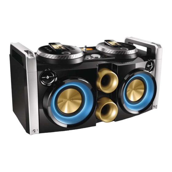
Mini Hi-Fi System
© Copyright 2011 Philips Consumer Electronics B.V. Eindhoven, The Netherlands.
All rights reserved. No part of this publication may be reproduced, stored in
a retrieval system or transmitted, in any form or by any means, electronic,
mechanical, photocopying, or otherwise without the prior permission of Philips.
Published by PZ-SL WK1209 BG LE
Version 1.2
TABLE OF CONTENTS
Technical Specifications ...........................................
Safety Instructions ........................................................
Location of PCB Boards ...........................................
Version Variation .....................................................
Measurement Setup .................................................
Service Aids ..............................................................
Rescue Mode & Repair Instructions....................
Disassembly Instructions & Service positions ...........
Block & Wiring Diagram ............................................
Main Board ...............................................................
AMP+Powder Board
........................................................
Mic Board.................................................................. 8
Key Board ................................................................
Jack Board ................................................................ 10
Ipod Board ................................................................
USB Board..................................................................
Exploded View...........................................................
Printed in the Netherlands
FWP3200D /05/12/93/85
Chapter
1-2
1-4
2-1
2-2
2-3
2-4
......
3
4
5
6
7
9
11
12
13
Subject to modication
3141 785 37322
Advertisement

Related Manuals for Philips FWP3200D/12


Summary of Contents for Philips FWP3200D/12
- Page 1 USB Board..............Exploded View............© Copyright 2011 Philips Consumer Electronics B.V. Eindhoven, The Netherlands. All rights reserved. No part of this publication may be reproduced, stored in a retrieval system or transmitted, in any form or by any means, electronic, mechanical, photocopying, or otherwise without the prior permission of Philips.
- Page 2 50 KHz...
-
Page 3: Safety Instructions
Make sure that, • Use only lead-free soldering tin Philips SAC305 with order during repair, you are connected with the same potential as code 0622 149 00106. If lead-free solder paste is required, the mass of the set by a wristband with resistance. - Page 4 Make sure that, • Use only lead-free soldering tin Philips SAC305 with order during repair, you are connected with the same potential as code 0622 149 00106. If lead-free solder paste is required, the mass of the set by a wristband with resistance.
- Page 5 1 - 5 Safety Instructions, Warnings, Notes, and Abbreviation List 2.3.5 Alternative BOM identification Abbreviation List It should be noted that on the European Service website, 0/6/12 SCART switch control signal on A/V “Alternative BOM” is referred to as “Design variant”. board.
- Page 6 Electro Magnetic Interference LORE LOcal REgression approximation EPLD Erasable Programmable Logic Device noise reduction Europe LG.Philips LCD (supplier) EXTernal (source), entering the set by Loudspeaker SCART or by cinches (jacks) LVDS Low Voltage Differential Signalling Fast BLanking: DC signal Mbps...
- Page 7 4.406250 MHz and 4.250000 MHz Sound Intermediate Frequency SMPS Switched Mode Power Supply System on Chip Sync On Green SOPS Self Oscillating Power Supply S/PDIF Sony Philips Digital InterFace SRAM Static RAM Service Reference Protocol Small Signal Board STBY STand-BY SVGA 800x600 (4:3)
- Page 9 FWP3200D : 220~240V 300W FWP3200D /05/12 /93/85 MLR+CLR AMP+Power Board MLR+CLR KEY +MIC Board MLR+CLR USB+Remote Board MLR+CLR Jack Board MLR+CLR IPod Board...
-
Page 10: Measurement Setup
Measurement Setup... - Page 27 7- 2 7- 2 Circuit Diagram - Part 1...
- Page 28 7 - 3 7 - 3 Circuit Diagram - Part 2...
- Page 29 7 - 4 7 - 4 Circuit Diagram - Part 3...
- Page 30 7 - 5 7 - 5 Circuit Diagram - Part 4...
-
Page 44: Ipod Board
11- 1 11- 1 Ipod Board TABLE OF CONTENTS Circuit Diagram ............................11-2 PCB Layout Top View ..........................11-3 PCB Layout Bottom View ......................... 11-4... - Page 53 14-1 Version History V1.0: initial release V1.1: Add /93 version V1.2: Add /85 version...
Need help?
Do you have a question about the FWP3200D/12 and is the answer not in the manual?
Questions and answers