Table of Contents
Advertisement
Quick Links
Advertisement
Table of Contents

Related Manuals for Dings DS-CLS10-FRS4


Summary of Contents for Dings DS-CLS10-FRS4
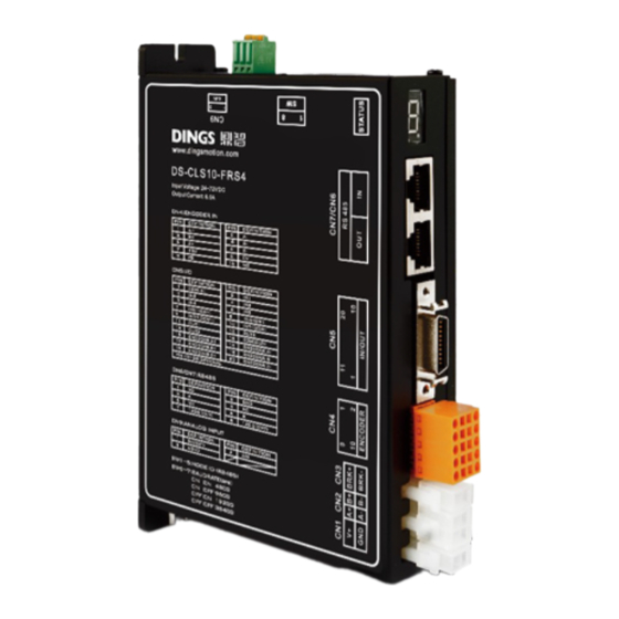
- Page 1 DS-CLS10-FRS4 Technical Manual VER 1.0 DS-CLS10-FRS4 page│1...
-
Page 2: Table Of Contents
Contents Table of Contents Click to return to table of contents Main Specifications…………………………………………………………………...…………………………3 Get Ready…………………………………………………………………... ……….……………………………… 2.1 Wiring……..…….…………………………..……………………………....…………………………4 The Connector Specifies the Table.………………………………………………....…………………….4 3.1 CN1 (power supply)………………………….……………………………………....……………….. 3.2 CN2 (motor wiring)…………..……………………………….…………………………... ……….………..4 3.3 CN3 (holding brake output)…..…………………….. …………….....……….………………..3.4 CN4 (encoder input)...……………………….………………………….....…………………….5 3.5 CN5 (I/O)……………………..……………………………….………………......…………..7 3.6 CN6 (IN) / CN7 (OUT)(RS485)..…………….……………………………………......…………... -
Page 3: Main Specifications
Main Specifications 1. Main Specifications Project Content Note Model DS-CLS10-FRS4 Input supply voltage DC 24V~72V Maximum output current 6.0A (0-peak) Control object motors 2-phase bipolar stepper motor with encoder Drive mode PWM constant current drive Input ・Pulse, direction input (configurable as digital input) ・Number input 7... -
Page 4: Get Ready
Get Ready / The Connector Specifies the Table 2. Get Ready * Be sure to do the following before turning on the power. 2.1 Wiring Be sure to make sure that you refer to the Description Connector Designation Table for wiring. CN1 :... -
Page 5: Cn3 (Holding Brake Output)
The Connector Specifies the Table 3.3 CN3 (holding brake output) Terminal number Icon Pin. Signal name BRK+ brake output is positive BRK - Negative brake output 3.4 CN4 (encoder input) Pin. Signal name Pin. Signal name Diagram Pay attention to the polarity of the encoder power supply when wiring Wire specifications: AWG28~AWG18 (multi-stranded wire) ... - Page 6 The Connector Specifies the Table ② You can open the terminal points with a standard screwdriver. The screwdriver is down and The screwdriver is down and right at the same time at the same time to the left Terminal points Terminal points ③...
-
Page 7: Cn5 (I/O)
The Connector Specifies the Table 3.5 CN5 (I/O) ICON : Pin. Signal name Pin. Signal name Pin. Signal name COM (IN) IN6- Encoder A+ IN7+ Encoder A- IN7- Encoder B+ OUT1 Encoder B- OUT2 Encoder Z+ OUT3 Encoder Z- IN6+ COM (OUT) Pin15~20 is the encoder output (differential output), which is optional and Notes... -
Page 8: Sw1 (Set The Switch)
3.7 SW1 (Setting Switch) 3.7.1 Mailing Address Users can control up to 30 DS-CLS10-FRS4 drivers simultaneously using the RS-485 bus. The drive communication address setting adopts a 5-digit DIP switch, The address setting range is 1-32, where address 32 is reserved for the system, when the drive address setting is greater than 31, it needs to be set and saved using the upper debugging software. -
Page 9: Input Loop Diagram
The Connector Specifies the Table 1C H 1D H 1E H 1F H customize customize 3.7.2 Communication Baud Rate DIP switch baud rate(bps) 4800 9600 19200 38400 3.7.3 Test Run The pilot run function is used to verify the performance of the drive. When the power is off, set the SW8 switch to ON. - Page 10 Input Loop Diagram 4.2 Command Pulse Input Loop (collector) AM26LS31 equivalent This product is compatible with+5V/+24V signal and there is no need to Notes connect current limit resistor in serial when 24V input. 4.3 Sensor, Digital Input Loop (contacts) 4.4 Sensor, Digital Input Loop (collector output) page│10...
-
Page 11: Output Loop Diagram
Output Loop Diagram 5. Output Loop Diagram 5.1 Digital Output Loop (relay connection) When the relay is connected, it is required to connect diodes at both ends Notes of the relay (such as IN4000 series) 5.2 Digital Output Loop (optocoupler connection) 5.3 Differential Output Loop (encoder output) The encoder output has no optocoupler isolation, please confirm again whether the wiring is correct and whether there is a short circuit before powering on, so... -
Page 12: Led Indicator
LED Indicator 6. LED Indicator 6.1 Status display Display Description Motor rotation display The light is on when the motor rotates and turns off when it stops Device enabled state The device enabling light is on, and the device disabling light is off Displayed in the command input The light is on in the command input CONNECT display... - Page 13 LED Indicator Alarm Alarm/warning Function Description code (Hex/Dec) Motor overcurrent Alarm AH (10) Motor phase current overcurrent or drive failure The motor is out of Alarm bH (12) The motor is not connected phase Spare Alarm CH (13) Factory reserved Undervoltage Alarm dH (14)
-
Page 14: Form Factor (Mm)
Form Factor / Control Parameters 7. Form Factor (mm) 8. Control Parameters Communication parameters are unofficial version, and some parameters are fixed Notes and not set open 8.1 Controller Basic Status (Class 01) range word content recount / unit 0100 Motor current Real-time motor current value 0.1%A... -
Page 15: Basic Parameter Settings (Class 02)
Control Parameters 0126 Physical location Run a live location pulse IO Select Multi-segment Run 0174 Paragraph Multi-segment writing error 0176 0178 Multi-stage operation No Data bits Bit7 …….. Bit1 Bit0 0135 Enter the port status Enter the port …….. Data bits Bit3 Bit2 Bit1... -
Page 16: Control Parameters (Class 06)
Control Parameters 0255 Location ring Kp Location ring Kp 0~30000 0~30000 Location out-of- 0258 In units of encoder resolution Encoder tolerance threshold resolution 8.4 Control Parameters (Class 05) word content recount range/unit 1~2000 0301 Startup frequency Default: 100 0.01~20rps 1~2000 0302 Stop frequency Default: 100... -
Page 17: Input Block Designation (Class 06)
Control Parameters moving distance during operation is invalid 3: Speed mode 4: Positive jogging 5: Reverse jogging 6: Decelerate and stop 7: Emergency stop 8: Set the current position, only when the motor stops 12: Return to the original point 13: Alarm clearance 14: Multi-segment data verification 15: Multi-segment data saving... -
Page 18: Output Block Designation (Class 07)
Control Parameters 15: Multi-segment data saving 16: Multi-segment data starts 17: Multi-segment data paused 18: End of multi-segment data 20: Enablement 25: Select Bit0 for the IO port configuration multi-segment 26: The IO port is configured with multiple segments to select Bit1 27: The IO port is configured with multiple segments to select Bit2... -
Page 19: Multi-Segment Position Mode (Class 08)
Control Parameters 0421 OUT2 function selection The setting content is the same as OUT 1 (default: 100) 100~104 0422 OUT3 function selection The setting content is the same as OUT 1 (default: 100) 100~104 0423 OUT 4 feature selection The setting content is the same as OUT 1 (default: 100) 100~104 Output port function selects 100 Universal digital output... - Page 20 Control Parameters Port selection corresponds to multiple segments Bit4 Bit3 Bit2 Bit1 Bit0 Location segment … … … … … … IO Select the port 1. Input port configuration multi-segment selection function 25~29: IO port configuration multi-se gment selection Bit0~Bit4 Input port configuration multi-segment start function 15: multi-segment data start 2.
- Page 21 Control Parameters Example: Writing, validating, and saving multi-segment parameters *Note: The data in the example is expressed in base 16 1. Multi-segment parameter settings [Command 1] the current line number 0: the fixed length speed is set to 1000, that is, 10rps, 04 00 00 02 00 36...
- Page 22 Control Parameters ④ : Write 3 data ⑤ : Write 6 bytes ⑥ : Data 1, relative to the 0x0041 of running the command (decimal means 65) ⑦ : Data 2,Data 03 E8 00 03 Converted to 00 03 03 E8 *Note: 4 bytes of data, the lower 16 bits First, the high 16 bits last Parameter A: The system reservation is set to 0 by default, do not set the value Parameter B: Wait for jump line 3, the current waiting command line is 2...
-
Page 23: Message Format
Control Parameters / Message Format 2. Multi-segment parameter checking 01 43 00 0E F8 26 ② ③ ④ ⑤ ① ① : 0x1 mailing address ② : MODBUS write command 0x06 ③ : Mailing address 0x0143 (decimal means 323, write communication command) ④... - Page 24 Message Format / MODBUS Transactions Therefore, for serial link communication, MODBUS PDU=256-server address (1 byte)-CRC (2-by te)=253 bytes. Thereby: RS232 / RS485 ADU = 253 bytes + server address (1 byte) + CRC (2 bytes) = 256 bytes.The MODBUS protocol defines three types of PDUs. They are: a.
-
Page 25: Modbus Transactions
MODBUS Transactions 10. MODBUS Transactions 10.1 Definition of MODBUS Transactions Figure 2:A state diagram of MODBUS transactions Once the server processes the request, establish a MODBUS response using the appropriate MODBUS server transaction. Based on the processing results, two types of responses can be established: 1. -
Page 26: Modbus Responds Normally
MODBUS Transactions 10.2 MODBUS Responds Normally Upper computer Drive Start the request Perform an action to Initiate the response Function code Data requests Opcode Data response Receive the response Figure 3: MODBUS transaction processing (error-free) 10.3 MODBUS exception response Upper computer Drive Start the request Errors detected in... -
Page 27: Definition Of Public Function Code And Description Of Function Code
Definition of Public Function Code and Description of Function Code 12. Definition of Public Function Code and Description of Function Code Function code code Subcode Hexadecimal Physical discrete input Read input discrete Read the coil Internal bits or physical access coils Enter memory Write a single coil Physical discrete input... - Page 28 Definition of Public Function Code and Description of Function Code Request Function code 1 byte 0x03 Start address 2 byte 0x0000 to 0xFFFF Number of registers 2 byte 1 to 125 (0x7D) Response Function code 1 byte 0x03 Number of bytes 1 byte 2 x N* Register value...
-
Page 29: 0X06) Write A Single Register
Definition of Public Function Code and Description of Function Code Figure 5: Read the state diagram of the hold-and-register register 12.2 06 (0x06) Write a Single Register In a remote device, use this function code to write a single hold register. The request PDU states the address of the register being written. - Page 30 Definition of Public Function Code and Description of Function Code Response Function code 1 byte 0x06 Register address 2 bytes 0x0000 to 0xFFFF Register value 2 bytes 0x0000 to 0xFFFF *N = Number of registers Mistake Error code 1 byte 0x86 Exception code 1 byte...
-
Page 31: 0X10) Write Multiple Registers
Definition of Public Function Code and Description of Function Code 12.3 16 (0x10) Write Multiple Registers In a remote device, use this function code to write blocks of continuous registers (1 to about 120 registers). The value written by the request is described in the request data field. Each register divides the data into two bytes. - Page 32 Figure 7: Writing a multi-register state diagram List of exception codes: MODBUS exception code Code Name Meaning For the server (or slave), the function code received in the query is not an allowable operation. This may be because the function code is only applicable to the new device and is not possible in the selected unit.
- Page 33 The value included in the query is not permissible to the server (or slave). This value indicates a failure in the remaining structure of the combined request, for example, the implied length is incorrect. It does Illegal data values not mean that, because the MODBUS protocol does not know the significance of any special value of any particular register, the data item in the register that is committed for storage has a value that is not expected by the application.
-
Page 34: Modbus Master Node Working Mode
MODBUS Master Node Working Mode / MODBUS Address Rules 13. MODBUS Master Node Working Mode The master node makes Modbus requests to child nodes in two modes: a. In unicast mode, the master node accesses a child node at a specific address, and after the child node receives and processes the request, the child node returns a packet (a reply) to the master node. -
Page 35: Master/Slave Communication Timing Diagram
Master / Slave Communication Timing Diagram 15. Master / Slave Communication Timing Diagram Figure 8: Master/slave communication timing diagram for various scenarios page│35... -
Page 36: Rtu Transmission Mode
RTU Transmission Mode 16. RTU Transmission Mode The format of each byte (11 bits) in RTU mode is: Encoding system: 8–bit binary Each 8-bit byte in the message contains two 4-digit hexadecimal characters (0–9, A–F) Bits per Byte: 1 starting bit 8 data bits, the least significant bit is sent first 1 bit as parity 1 Stop bit... -
Page 37: Crc Check
CRC Check 17. CRC Check CRC contains a 16-bit value consisting of two 8-bit bytes. The CRC field is appended to the message as the last domain of the message. After calculation, the low byte is appended first, followed by the high byte. The CRC high byte is the last subsection of the message sent. - Page 38 CRC Check The function takes two parameters: unsigned char *puchMsg; A pointer to a buffer containing the binary datagram used to generate the unsigned short usDataLen; The number of bytes in the message buffer CRC generation function unsigned short CRC16 ( puchMsg,usDataLen ) /* The function is returned as an unsigned short type CRC */ unsigned char *puchMsg ;...
- Page 39 CRC Check 0x80, 0x41, 0x01, 0xC0, 0x80, 0x41, 0x00, 0xC1, 0x81, 0x40, 0x01, 0xC0, 0x80, 0x41, 0x00, 0xC1, 0x81, 0x40, 0x00, 0xC1, 0x81, 0x40, 0x01, 0xC0, 0x80, 0x41, 0x01, 0xC0, 0x80, 0x41, 0x00, 0xC1, 0x81, 0x40, 0x00, 0xC1, 0x81, 0x40, 0x01, 0xC0, 0x80, 0x41, 0x00, 0xC1, 0x81, 0x40, 0x01, 0xC0, 0x80, 0x41, 0x01, 0xC0, 0x80, 0x41, 0 x00, 0xC1, 0x81, 0x40, 0x00, 0xC1, 0x81, 0x40, 0x01,...
- Page 40 CRC Check 0x37, 0xF5, 0x35, 0x34, 0xF4, 0x3C, 0xFC, 0xFD, 0x3D, 0xFF, 0x3F, 0x3E, 0xFE, 0xFA, 0x3A, 0x3B, 0xFB, 0x39, 0xF9, 0xF8, 0x38, 0x28, 0xE8, 0xE9, 0x29, 0xEB, 0x2B, 0x2A, 0xEA, 0xEE, 0x2E, 0x2F, 0xEF, 0x2D, 0xED, 0xEC, 0x2C, 0xE4, 0x24, 0x25, 0xE5, 0x27, 0xE7, 0xE6, 0x26, 0x22, 0xE2, 0xE3, 0x23, 0xE1, 0x21, 0x20, 0xE0, 0xA0, 0x60, 0x61, 0xA1, 0x63, 0xA3, 0xA2,...
-
Page 41: Line-Modbus Definition
Line-MODBUS Definition 18. Line-MODBUS Definition MODBUS solutions on serial links should implement a "2-wire" electrical interface in accordance with the EIA/TIA-485 standard. Figure 11: 2-Line general topology page│41... - Page 42 International Customer Person in Charge : Daniel Jang daniel@dingsmotion.com Building 1#, 355 Longjin Road, Changzhou Economic Development Zone, Jiangsu, China +86-519-85177826, 85177827 North America Customer Person in Charge : Nicolas Ha sales@dingsmotionusa.com 335 Cochrane Circle Morgan Hill, CA 95037 +1-408-612-4970 China Customer +86-0519-8517 7825...
Need help?
Do you have a question about the DS-CLS10-FRS4 and is the answer not in the manual?
Questions and answers