Advertisement
Quick Links
NIBP SINGLEWIDE MODULE
INTRODUCTION
This area contains component information about the
singlewide Model 7300 Non-Invasive Blood
Pressure (NIBP) Module. The singlewide NIBP
module monitors blood pressure noninvasively,
using the oscillometric method that measures the
amplitude of the pressure oscillations within the
blood pressure cuff. Systolic pressure, diastolic
pressure, mean arterial pressure, and cuff pressure
are all measured by the module. Heart rate values
are also derived from the pulse rate determined by
the oscillometric blood pressure measurement
technique.
Advertisement

Related Manuals for Dinamap 7300


Summary of Contents for Dinamap 7300
- Page 1 NIBP SINGLEWIDE MODULE INTRODUCTION This area contains component information about the singlewide Model 7300 Non-Invasive Blood Pressure (NIBP) Module. The singlewide NIBP module monitors blood pressure noninvasively, using the oscillometric method that measures the amplitude of the pressure oscillations within the blood pressure cuff.
-
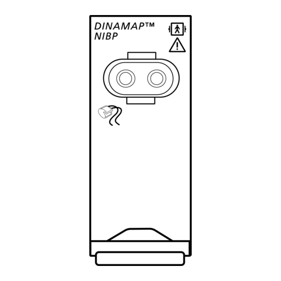
Page 2: Physical Description
PHYSICAL DESCRIPTION The singlewide version of the NIBP module, shown in FO-42B, occupies a single module slot. The module consists of two PWAs, interconnect cabling, a pump manifold assembly, a cuff manifold assembly, and a mechanical enclosure. Digital PWA 315459 includes an interface to the PNet communication bus, module core logic, and the analog to digital conversion subsystem. - Page 3 FUNCTIONAL PRINCIPLES OF OPERATION A schematic diagram of the pneumatics system is shown in Figure 4-1. It illustrates all connections to valves, transducers, and pump. The pump draws air in and forces it through the check valve to the system manifold.
- Page 4 Figure 4-1. NIBP Singlewide Pneumatics Schematic...
- Page 5 Analog Circuits The analog circuits consist of cuff measurement, overpressure, and pneumatics circuits. Transducers XD1 and XD2 shown on sheet 1 receive excitation voltage from +10V references. Differential signal XD1SIG+/- from transducer XD1 representing blood pressure is applied to the analog multiplexer through the pre-amp and low pass filter.
- Page 6 The pneumatics latch and solenoid drive circuits control the pump drive and the dump and deflate/zero valves. Pneumatic reset or failsafe signals from the CPU shut down the pump and open the dump valve. Signal PUMPC measures pump current. This allows the CPU to monitor when the pump is running.
- Page 7 COMPONENT PRINCIPLES OF OPERATION The following paragraphs describe the function of the two rigid PWAs. The NIBP analog PWA provides the circuitry for the excitation, amplification, and signal conditioning (filtering) for measurement of non-invasive blood pressure within the NIBP module. Also included are the associated circuitry for a separate, independent direct overpressure interactive channel.
- Page 8 Table 42-1. CPU Register Mapping (Continued) Mapping of Bits in Port B: Signal Type Comment PB(0) LATCH_OVP input Latched Overpressure, normal =1 PB(1) POTCS-0 output init_val =1 PB(2) POTINC-0 output init_val = 1 PB(3) POTU~D-0 output init_val = 0 PB(4) TOUT1-0 output (Not used)
- Page 9 Analog PWA The NIBP analog PWA includes four functional circuits: analog mux, filtered NIBP, overpressure, and pneumatics. Analog Mux The analog mux functional block consists of a single eight-to-one analog multliplexer and includes an output buffer amplifer. Data is transferred to the digital card via a single analog channel BUF_ANA_MUX (MUX_OUT) on J100, Pin2.
- Page 10 Filtered NIBP The filtered NIBP functional block consists of signal conditional circuitry required to measure the cuff oscillatory pressure (PT1) and acquire a blood pressure determination. Circuitry for offset, voltage clamping, and test pulse injection are also included. The excitation voltage for the cuff transducer is derived from the analog-to-digital converter, located on the digital PWA.
- Page 11 The blood pressure algorithm requires the ability to initialize (clamp) the high pass filter in the process of separating and measuring the pulse signal. Two clamps are used in this process. FLT_Clamp-0 provides a clamp to ground of the input to the second stage and also clamps the output buffer to a +200 mV offset reference voltage.
- Page 12 Table 42-4. PT1 Output Characteristics Operating Conditions: Power Supply Voltages=+5V+/-5%, +12V+/-5%, -12V+/-5% Characteristics Symbol Units Gain* 88.83 91.89 94.96 Offset Voff Offset, including AD2 ref Voff XDCR,FSS VFSS 38.5 41.5 XDCR, OFFSET VFSS -1.0 +1.0 Linearity, with XDCR -0.25 +0.25 %FSS Full Scale Scan, with XDCR VFSS...
- Page 13 Table 42-5. PT2 Output Characteristics Operating Conditions: Power Supply Voltages = +5V+/-5%, +12V+/-5%, -12V+/-5% Characteristics Symbol Units Gain* 90.70 91.89 93.08 Offset Voff Linearity, with XDCR -0.25 +0.25 %FSS Full Scale Scan, with XDCR VFSS 3555 3676 3904 Offset Voltage, with XDCR Voff *Gain of signal [range 1-40mv] injected between pins J103-Pin3 and J103-Pin5 Table 42-6.
- Page 14 Threshold trimming is accomplished by controlling three input signals: CS-0 (Chip Select), U_D-0 (Direction: Up or Down), and INC-0 (Increment or Decrement). A interlock jumper, JP1, which connects CS-0 to the board edge pin, is required to be installed or threshold adjustment is inhibited. The E2POT incorporates a storage mode that permits maintaining the threshold setting once adjusted.
- Page 15 Table 42-7. Latched Control Signals and Decode Matrix Operating Conditions: RESET-0 =1; PNEURESET=1; FAILSAFE-0 =1; FLT_0VP-0=1 Pneu_Enab Data LSEL0 LSEL1 LSEL2 Signal Value Description ¥ TK_Inflate_Val Open Not Used Closed ¥ Cuff_Deflate_Val Closed When open, deflates Cuff Open ¥ Cuff_Dump_Val Open When closed, Closed...
- Page 16 Table 42-9. Processor Pneureset State Operating Conditions: RESET=1; FAILSAFE-0 =1; FLT_0VP-0=1 PneuReset Data LSEL0 LSEL1 LSEL2 Signal Value Description (Reset Condition) § TK_Inflate_Val Vn+1 = Vn Not Used § Cuff_Deflate_Val Vn+1 = Vn Same, before and after pulse § Cuff_Dump_Val Pn+1 = Pn Same, before and after pulse §...
- Page 17 Digital PWA The NIBP digital PWA block diagram is shown in sheet one of hierarchical schematic SC315-459. It includes the core logic blocks PNET IF (PNET Interface), RESET-FS (Reset - FailSafe), UP8-144 (microprocessor-8 bit), EIGHT BIT MEMORY, and LOGIC ANALYZER TEST IF. Unique to this PWA is the analog-to-digital converter functional block.
- Page 18 Processor Digital I/O and Chip Select Assignments 68302 PORT SIGNAL TYPE COMMENT debug serial SCC2 RXD output debug serial SCC2 TXD input SERIAL EEPROM CS output undefined PNEUMATIC RESET output ASYNC_EN (PNET) Motor Power Control output LATCHED_OVC input Latched Motor Overcurrent Indication DATA FROM ISO (FOR FUTURE TEMP I/F) DATA TO ISO...
- Page 19 Core Logic The core logic is shown on sheets 2 through 7 of the schematic. The core logic provides communication between the system host and Module through the PNet synchronous serial interface. The Module is an 8-bit version of the core logic, with one 128Kx8 RAM and 128Kx8 ROM device.
- Page 20 The NIBP Module is designed to be hot-plugged, or inserted and removed from powered systems. Ground pins 1 and 2 are longer than the other connector pins, thus they make first and break last to protect circuitry. This is partially because of protective impedance located on the system backplane, in series with the Modules +5V and +12V power.
- Page 21 The Module present output, M_PRESENT is connected to M_SELECT through diode CR1 to allow a means of determining if the Module is plugged into an instrument. When M_SELECT is asserted (pulled hi) M_PRESENT is hi true. Module transmitter open collector signal TXOC-0 from Q1 signifies the Module transmitter is enabled.
- Page 22 Microprocessor. The core logic design is based around the 68302 microprocessor (U10) shown on sheet 4 of the schematic. The 68302 combines a 68000 core with a three channel communication processor, and system integration circuits. The left side of the CPU contains clock interfaces to/from the PNet, port A, and port B to various circuits in the core logic, reset, and halt interface.
- Page 23 Program Memory. Program memory consists of 8-bit flash ROM U11 shown on sheet 5 of the schematic. The ROM is configured for 128Kx8 (1024k bit). The ROM is not socketed and cannot be removed for programming. The ROM can be flash- programmed via the logic analyzer interface or the PNET connector.
- Page 24 The LA/T connector pinouts are as follows: NAME NAME 1,69 2,28,45,46,7 DTACK-0 AS-0 UDS-0 DS-0 BGACK-0 DEBUG TXD DEBUGRXD EXROMCS-0 PRGM_EN DISCPU T1_IN...
-
Page 25: Disassembly Procedure
DISASSEMBLY PROCEDURE STATIC DISCHARGE CAUTION Do not attempt to service unit without static discharge protection. Workstations and personnel must be properly grounded, or damage to equipment will result. 1. Remove two 4-40 x 5-1/8" screws from the rear of the Module. Remove rear cover. 2. -
Page 26: Reassembly Procedure
REASSEMBLY PROCEDURE 1. If disassembled, prepare pneumatic manifold and pump assembly (5) and hose (21) as shown in FO-42B. 2. Attach analog PWA (7) by aligning manifold standoff with grommet of PWA and aligning edge of PWA with pump assembly shock mount. 3. -
Page 27: Parts Lists
FO-42C NIBP Digital PWA 315-459 Table 42-13 FO-42D Pneumatic Manifold Table 42-14 FO-42E Assembly 320-646 Table 42-11. Top Assembly 7300 Parts List Item Description Part No. SCREW, 2-56X3/16 PNH PHH SST 719-237 PWA, FLEX, CUFF PRESSURE, NIBP 313-114 PNEUMATIC MANIFOLD ASSY, SINGLE-WIDE... - Page 28 Table 42-12. NIBP Analog PWA 315-452 Parts List Item Description Part No. C2-19,21-31, CAP,CER,SMD,0805,X7R,10%,50V,0.10 UF 605-533 33,44-53,55, C35, 36 CAP,METAL POLYESTER, 1.0 UF 5%, 40V SMD 603-221 CAP,2917/DTANT,16V,20%,22UF 606-110 C38-39 CAP,CERAMIC,SMD,X7R,50V,1.0 UF 605-361 CR1-5 DIO SWI, 200 MA, 70V, SMD 610-114 DIODE 1AMP, 50V GEN PUR SMT 610-123...
- Page 29 Table 42-13. NIBP Digital PWA 315-459 Parts List Item Description Part No. C2,3 CAP,CER,SMD,0603,NPO,10%,50V,27 PF 605-718 C4-14,16,102, CAP,CER,SMD,0805,X7R,10%,50V,0.10 UF 605-533 104,106108, 113,114 C101,103,105 CAP,2917/D,TANT,35V,20%,10 UF 606-188 ,109 C112 CAP,2917/D,TANT,35V,20%,4.7UF 606-186 C115 CAP,CERAMIC,SMD,X7R,50V MIN,1000 PF 605-209 CR1,13 DIODE, SCHOTTKY, 30V, 200MW, SOT-23 611-137 CR2-7,10,11 DIODE, DUAL SERIES SMT SOT-23...
- Page 30 Table 42-13. NIBP Digital PWA 315-459 Parts List (Continued) Item Description Part No. IC, 128K X 8-BIT 5V FLASH ROM CMOS SMT 692-195 IC,74HC03 QUAD 2 IN.NAND,CMOS SUF MT 692-139 U7,8 IC, CMOS LTC1485, DIFF BUS XCEIVER SO8 692-225 IC, POWER SUPPLY MONT WITH RESET SMT 694-118 IC, 68302 MICROPROC., 20MHZ SMT 694-136...
- Page 31 J103 +10V AIN6 PT1_REF XD1EX+ PRESSURE REFERENCE TRANSDUCER AIN5 XD1SIG+ PRE-AMP ANALOG XD1SIG- LOW-PASS AIN4 U4, U13 FPT1 FILTER U9,U12 XD1EX- U8, U5 AIN3 AIN7 PUMPC AIN2 AIN1 TH_VREF GAIN CONTROL FLT_CLAMP J105 +10V PT2_REF REFERENCE XD2EX+ U2, U3 PRESSURE TRANSDUCER BUFFER XD2SIG+...
- Page 32 FLT_CLAMP PNEUMATICS INFLATE DECODE LOGIC DEFLATE ADULT-0 DUMP DEFLATE_VAL J102 PUMP_ON PNEUMATICS DUMP_VAL LATCH & SOLENOID TO SHEET 1 DRIVE FLT_OVP-0 U16,Q1,Q2 PUMP- VALVE DEFLATE/ZERO PUMP DRIVE PUMP VALVE PUMP+ Q3-B, Q5,U12 VALVE_PWR +12V PUMPC PART J100 NIBP ANALOG PWA 11 12 23 NIBP DIGITAL PWA PROGRAM...
- Page 33 FO-42B. Top Assembly 7300...
- Page 34 FO-42C. NIBP Analog PWA 315-452 (1 of 2)
- Page 35 FO-42C. NIBP Analog PWA 315-452 (2 of 2)
- Page 36 FO-42D. NIBP Digital PWA 315-459 (1 of 2)
- Page 37 FO-42D. NIBP Digital PWA 315-459 (2 of 2)
- Page 38 APPLY RUBBER LUBRICANT TO O-RING AS REQUIRED. FO-42E. Pneumatic Manifold Assembly 320-646...
- Page 39 SC315-459 A NIBP Digital PWA Schematic (1 of 7)
- Page 40 SC315-459 A NIBP Digital PWA Schematic (2 of 7)
- Page 41 SC315-459 A NIBP Digital PWA Schematic (3 of 7)
- Page 42 SC315-459 A NIBP Digital PWA Schematic (4 of 7)
- Page 43 SC315-459 A NIBP Digital PWA Schematic (5 of 7)
- Page 44 SC315-459 A NIBP Digital PWA Schematic (6 of 7)
- Page 45 SC315-459 A NIBP Digital PWA Schematic (7 of 7)
- Page 46 SC315-452 A NIBP Analog PWA Schematic (1 of 5)
- Page 47 SC315-452 A NIBP Analog PWA Schematic (2 of 5)
- Page 48 SC315-452 A NIBP Analog PWA Schematic (3 of 5)
- Page 49 SC315-452 A NIBP Analog PWA Schematic (4 of 5)
- Page 50 SC315-452 A NIBP Analog PWA Schematic (5 of 5)
Need help?
Do you have a question about the 7300 and is the answer not in the manual?
Questions and answers