Table of Contents
Advertisement
Quick Links
SERVICE MANUAL
Ver 1.0 2004. 10
• AVJ-X33 is composed of the following models.
As service manuals are issued for each component model,
please refer to them.
COMPONENT MODEL NAME
DVD RECEIVER
SATELLITE SPEAKER
SUB WOOFER
SPECIFICATIONS
Supplied accessories
Speakers (5)
Subwoofer (1)
Remote Commander (remote) RM-Z20012 (1)
Operating Instructions (1)
Speakers-Connection and Installation (card) (1)
Video cable (1) (E3, E32, AUS, SP)
Speaker cables (6)
Size AAA (R03) batteries (2)
AM loop antenna (1)
FM antenna (1)
Ferrite core (1)
Foot pads (20)
Plug adapter (1) (E3, E32, SP)
Design and specifications are subject to change without
notice.
• Abbreviation
AUS : Australian model
E3 : 240 V AC area in E model
E32 : 110 – 240 V AC area in E model
CET : East European & Russian model
RU : Russian model
SP : Singapore model
Sony Corporation
9-879-236-01
2004J04-1
Personal Audio Company
© 2004. 10
Published by Sony Engineering Corporation
AVJ-X33
CX-VX33
SSX-VX33S
SSX-VX33W
ACCESSORIES
Part No.
2-050-638-21 MANUAL, INSTRUCTION (ENGLISH) (UK)
2-050-638-41 MANUAL, INSTRUCTION (ENGLISH,RUSSIAN) (RU)
2-050-638-51 MANUAL, INSTRUCTION (ENGLISH,FRENCH,SPANISH,
2-050-638-61 MANUAL, INSTRUCTION (ENGLISH) (AUS)
2-050-638-71 MANUAL, INSTRUCTION (ENGLISH,FRENCH,ARABIC,
2-050-638-81 MANUAL, INSTRUCTION (ENGLISH,SPANISH,FRENCH)
2-159-427-01 MANUAL, INSTRUCTION (ENGLISH,FRENCH,SPANISH)
2-159-427-11 MANUAL, INSTRUCTION (GERMAN,ITALIAN,POLISH)
2-159-427-21 MANUAL, INSTRUCTION (HUNGARIAN,CZECH) (CET)
2-159-427-31 MANUAL, INSTRUCTION (ENGLISH,FRENCH,SPANISH)
2-159-427-41 MANUAL, INSTRUCTION (GERMAN,ITALIAN,POLISH)
2-159-427-51 MANUAL, INSTRUCTION (HUNGARIAN,CZECH) (AEP)
9-885-069-40 SPEAKER CABLE ASSY (NLB1-91-001)
9-885-069-41 ATENNA, FM
9-885-069-42 ANTENNA, AM
9-885-069-60 CABLE, VIDEO (E3,E32,AUS,SP)
9-885-071-46 REMOTE COMMANDER (RM-Z20012)
DVD HOME THEATRE SYSTEM
AVJ-X33
AEP Model
Australian Model
Description
TRADITIONAL CHINESE) (SP)
UK Model
E Model
Remark
PERSIAN) (E3)
(E32)
(CET)
(CET)
(AEP)
(AEP)
Advertisement
Table of Contents

Subscribe to Our Youtube Channel
Related Manuals for Sony AIWA AVJ-X33


Summary of Contents for Sony AIWA AVJ-X33
- Page 1 2-159-427-51 MANUAL, INSTRUCTION (HUNGARIAN,CZECH) (AEP) 9-885-069-40 SPEAKER CABLE ASSY (NLB1-91-001) 9-885-069-41 ATENNA, FM 9-885-069-42 ANTENNA, AM 9-885-069-60 CABLE, VIDEO (E3,E32,AUS,SP) 9-885-071-46 REMOTE COMMANDER (RM-Z20012) DVD HOME THEATRE SYSTEM Sony Corporation 9-879-236-01 2004J04-1 Personal Audio Company © 2004. 10 Published by Sony Engineering Corporation...
- Page 2 AVJ-X33 REVISION HISTORY Clicking the version allows you to jump to the revised page. Also, clicking the version at the upper on the revised page allows you to jump to the next revised page. Ver. Date Description of Revision 2004. 10...
- Page 3 20 kHz LPF/A-Filter) DVD RECEIVER Dynamic range (audio) More than 70 dB Harmonic distortion 0.5% (1 kHz, at 12 W position) (audio) (20 kHz LPF/A-Filter) Sony Corporation 9-879-238-05 2005J04-1 Personal Audio Division © 2005. 10 Published by Sony Engineering Corporation...
- Page 4 COMPONENTS IDENTIFIED BY MARK 0 OR DOTTED LINE WITH MARK 0 ON THE SCHEMATIC DIAGRAMS AND IN THE PARTS LIST ARE CRITICAL TO SAFE OPERATION. REPLACE THESE COMPONENTS WITH SONY PARTS WHOSE PART NUMBERS APPEAR AS SHOWN IN THIS MANUAL OR IN SUPPLEMENTS PUBLISHED BY SONY.
-
Page 5: Table Of Contents
CX-VX33 Ver. 1.1 TABLE OF CONTENTS CAUTION Use of controls or adjustments or performance of procedures 1. GENERAL other than those specified herein may result in hazardous Front Panel Controls ..............4 radiation exposure. Display Window Indicators ............. 5 Remote Control ............... 6 Rear Panel Connections (AEP, UK, CET, RU Model) .... -
Page 6: General
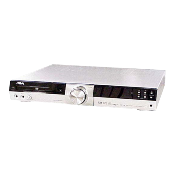
CX-VX33 SECTION 1 GENERAL This section is extracted from instruction manual. Front Panel Controls ? / 1 (POWER) indicator STOP (x) Switches the DVD Receiver ON and OFF. Stops playback of a disc. STANDBY indicator PAUSE (X) Lights red when the receiver Pause playback of a disc temporarily. -
Page 7: Display Window Indicators
CX-VX33 Display Window Indicators Playing status. Repeat playback mode indicators. Indicates the unit is radio mode. Indicates the unit is stereo mode. Lights up when the DVD Receiver tunes in a station. CD disc inserted. MP3 disc inserted. VCD2.0 disc inserted. SLEEP timer indication DISC TUNED... -
Page 8: Remote Control
CX-VX33 Remote Control OPEN/CLOSE TV ? / 1 Opens and closes the disc tray. Switches TV ON and OFF. TV/VIDEO ? / 1 Switches DVD Receiver ON and OFF. Selects the TV’s source. 0-9 numerical buttons DISPLAY To display remaining time between Selects numbered options in a menu. -
Page 9: Rear Panel Connections (Aep, Uk, Cet, Ru Model)
CX-VX33 AEP, UK, CET, RU MODEL Rear Panel Connections AC Power Cord Plug into the power source. EURO AV OUTPUT (TO TV) Connect to your TV set. MONITOR OUT (VIDEO) Connect to a TV with video input. VIDEO (AUDIO IN R/L) Connect the audio output of an external source (VCR, LD player, etc). -
Page 10: Rear Panel Connections (E3, E32, Aus, Sp Model)
CX-VX33 E3, E32, AUS, SP MODEL Rear Panel Connections AC Power Cord Plug into the power source. SPEAKER CONNECTORS Connect the six supplied MONITOR OUT (VIDEO) speakers to these terminals. Connect to a TV with video input. VIDEO (AUDIO IN L/R) Connect the audio output of an external source (VCR, LD player, etc). -
Page 11: Disassembly
CX-VX33 Ver. 1.1 SECTION 2 DISASSEMBLY Note : This set can be disassemble according to the following sequence. 2-1. TOP COVER (Page 9) 2-2. FRONT PANEL ASSY 2-4. REAR PANEL SECTION (Page 10) (Page 11) 2-3. DVD MECHANISM DECK 2-5. SMPS BOARD (Page 10) (Page 11) -
Page 12: Front Panel Assy
CX-VX33 Ver. 1.1 2-2. FRONT PANEL ASSY 1 two screws 2 shield (barrier) 3 PN202 (5P) 6 Remove the ferrite core attached to the power cord. 8 claw qa claw 4 PN101 (23 core) 7 claw 5 PN102 (24 core) 9 claw qs three claws 0 two claws... -
Page 13: Rear Panel Section
CX-VX33 Ver. 1.1 2-4. REAR PANEL SECTION 4 screw 5 two screws 6 two screws 3 PN103 (12 core) 7 two screws 8 screw 9 rear panel section 1 Pull up the two claws pressing the power cord. 2 PN901 (2P) 2-5. -
Page 14: Dvd Board
CX-VX33 Ver. 1.1 2-6. DVD BOARD 2 two screws 1 two screws CN902 CN901 3 SMPS board 2-7. MAIN BOARD 2 screw 1 two screws 3 screw 4 MAIN board... -
Page 15: Base Unit
CX-VX33 Ver. 1.1 2-8. BASE UNIT 1 two drawing screws 2 holder assy 8 two rubbers 6 two drawing screws 7 two drawing screws 9 two rubbers 0 base unit 5 tray assy 3 guide... -
Page 16: Electrical Troubleshooting Guide
CX-VX33 Ver. 1.1 SECTION 3 ELECTRICAL TROUBLESHOOTING GUIDE 3-1. AUDIO PART 1. Power check flow INSERT POWER CORD. TURN ON CHECK POWER PLUG THE RED LED? AND POWER SUPPLY CIRCUIT . TURN POWER ON. IS POWER ON? CHECK POWER SUPPLY CIRCUIT . DOES INITIAL CHECK LASER CIRCUIT . - Page 17 CX-VX33 Ver. 1.1 2. AUDIO µ.COM CIRCUIT POWER ON Does other function Does CD/DVD name appear at FLD? appear at FLD? Does it appear Does LOADING DVD Error at appear at FLD? FLD? Check Does no Disc or Connector(PN902)if Reconnect it. Time appear at FLD? is normally.
- Page 18 CX-VX33 Ver. 1.1 3. FRONT CIRCUIT (1/2)
- Page 19 CX-VX33 Ver. 1.1 4. FRONT CIRCUIT (2/2)
-
Page 20: Dvd Part
CX-VX33 Ver. 1.1 3-2. DVD PART 1. Power check flow Does other function name appear at FLD? PDM02 PDM01 PDA02 PDA03 PDA01... - Page 21 CX-VX33 Ver. 1.1 2. Test & debug flow...
- Page 22 CX-VX33 Ver. 1.1...
- Page 23 CX-VX33 Ver. 1.1...
- Page 24 CX-VX33 Ver. 1.1...
- Page 25 CX-VX33 Ver. 1.1...
- Page 26 CX-VX33 Ver. 1.1...
-
Page 27: Details And Waveforms On System Test And Debugging
CX-VX33 Ver. 1.1 3-3. DETAILS AND WAVEFORMS ON SYSTEM TEST AND DEBUGGING 1. SYSTEM 27MHz CLOCK, RESET, FLASH R/W SIGNAL 1) MT1379 main clock is at 27MHz (X501) 2) MT1336 reset is high active... - Page 28 CX-VX33 Ver. 1.1 3) RS232 waveform during procedure (Downloading) 4) Flash R/W enable signal during download (Downloading)
- Page 29 CX-VX33 Ver. 1.1 2. SDRAM CLOCK 1) MT1379 main clock is at 27MHz (X501) 3. TRAY OPEN/CLOSE SIGNAL 1) Tray open/close waveform...
- Page 30 CX-VX33 Ver. 1.1 2) Tray close waveform 3) Tray open waveform...
- Page 31 CX-VX33 Ver. 1.1 4. SLED CONTROL RELATED SIGNAL (NO DISC CONDITION) 5. LENS CONTROL RELATED SIGNAL (NO DISC CONDITION)
- Page 32 CX-VX33 Ver. 1.1 6. LASER POWER CONTROL RELATED SIGNAL (NO DISC CONDITION) 7. DISC TYPE JUDGEMENT WAVEFORM...
- Page 33 CX-VX33 Ver. 1.1...
- Page 34 CX-VX33 Ver. 1.1 8. FOCUS ON WAVEFORM...
- Page 35 CX-VX33 Ver. 1.1 9. SPINDLE CONTROL WAVEFORM (NO DISC CONDITION)
- Page 36 CX-VX33 Ver. 1.1 10. TRACKING CONTROL RELATED SIGNAL (SYSTEM CHECKING)
- Page 37 CX-VX33 Ver. 1.1 11. RF WAVEFORM 12. MT1379 AUDIO OPTICAL AND COAXIAL OUTPUT (ASPDIF)
- Page 38 CX-VX33 Ver. 1.1 13. MT1379 VIDEO OUTPUT WAVEFORM 1) Full colorbar signal (CVBS) 2) Y...
- Page 39 CX-VX33 Ver. 1.1 3) C 14. AUDIO OUTPUT FORM AUDIO DAC 1) Audio related Signal...
-
Page 40: Test Mode
CX-VX33 Ver. 1.1 SECTION 4 TEST MODE DVD Processor Reset Procedure: 1. Press the DVD SETUP key on the remote commander to enter the set up screen. The following SET UP menu is dis- played. 2. Move the cursor to [TV Aspect,16:9 Wide] on the screen. 3. -
Page 41: Electrical Adjustment
CX-VX33 Ver. 1.1 SECTION 5 ELECTRICAL ADJUSTMENT [RFMON Level Check] Connection: oscilloscope DVD board PDM01 pin 2 (RFOUT) – PDM01 pin 6 (GND PD) Procedure: 1. Connect an oscilloscope to PDM01 pin 2 (RFOUT) and PDM01 pin 6 (GND PD) on the DVD board. 2. - Page 42 CX-VX33 Ver. 1.1 MEMO...
-
Page 43: Diagrams
CX-VX33 Ver. 1.1 SECTION 6 DIAGRAMS 6-1. BLOCK DIAGRAM — DVD SECTION — IC201 OPTICAL Q501 CD/DVD RF AMP, PICK-UP SERVO CONTROL BLOCK RF OUT 96 DVDRFIP IC501 MPEG & VIDEO PROCESS IC5C1 E3,E32,AUS,SP MODEL RFOP RFIP DVD VIDEO DRIVE RFON RFIN JK601 (1/2) -
Page 44: Block Diagram -Audio Section
CX-VX33 Ver. 1.1 6-2. BLOCK DIAGRAM — AUDIO SECTION — IC301 IC502 DIGITAL AUDIO PROCESSOR HEADPHONE AMP Q503 JK001 PWMHPL+ R-CH MUTE PHONES PWMHPL– 45 PWMHPR+ R-CH PWMHPR– 40 R-CH Q609,983 MUTE TUNER/POWER MUTE CONTROL SECTION (Page 43) IC710 ADATA0 SSDIN0 AUDIO POWER DRIVE ADATA1... -
Page 45: Block Diagram -Tuner/Power Section
CX-VX33 Ver. 1.1 6-3. BLOCK DIAGRAM — TUNER/POWER SECTION — (Page 42) AUDIO MUTE PN103 SECTION T AUDIO L OUT AUDIO D921 SECTION (Page 42) AUDIO T AUDIO R OUT P.SENS R-CH (Page 42) IC101 SECTION (3/3) SYSTEM CONTROL,FL DRIVER 5.6VCPU IC921 TM301... - Page 46 CX-VX33 Ver. 1.1 • Circuit Boards Location • Waveforms — DVD Board — — MAIN Board — DVD board MOTOR board IC201 qk (FEO) IC101 qh (CF2) JACK (AUDIO) board MAIN board 0.2Vp-p 1.6Vp-p 9.8304MHz 100mV/DIV, 1ms/DIV 1V/DIV, 10ns/DIV IC201 wa (TEO) IC301 ih (CLK IN) KEY board SMPS board...
-
Page 47: Printed Wiring Boards -Dvd Section (1/2)
CX-VX33 Ver. 1.1 6-4. PRINTED WIRING BOARDS — DVD SECTION (1/2) — • Refer to page 44 for Circuit Boards Location. : Uses unleaded solder. DVD BOARD (SIDE A) C519 C518 TP553 R735 R737 TP_URB# R521 TP_UWR# E3,E32,AUS,SP R522 MODEL TP_MA11 TP_ALE C5C8... -
Page 48: Printed Wiring Board -Dvd Section (2/2)
CX-VX33 Ver. 1.1 6-5. PRINTED WIRING BOARD — DVD SECTION (2/2) — • Refer to page 44 for Circuit Boards Location. : Uses unleaded solder. DVD BOARD (SIDE B) (D/L PORT) C5C9 C555 TP505 TP515 C5C2 TP514 TP520 TP506 TP517 TP512 TP502 TP501... -
Page 49: Schematic Diagram -Dvd Section (1/3)
CX-VX33 Ver. 1.1 6-6. SCHEMATIC DIAGRAM — DVD SECTION (1/3) — • Refer to page 44 for Waveforms. R256 TP224 R201 RVCC C281 C280 R257 Q201 C206 C201 R202 C291 R203 Q203 C279 Q202 C251 PDM01 R255 R209 R204 R254 C252 TP206 C278... -
Page 50: Schematic Diagram -Dvd Section (2/3)
CX-VX33 Ver. 1.1 6-7. SCHEMATIC DIAGRAM — DVD SECTION (2/3) — • Refer to page 44 for Waveforms and page 63 for IC Block Diagrams. IC B/D R570 L502 C583 C528 C534 C582 C527 C555 C563 L501 C532 C533 C531 C530 C554 IC506... -
Page 51: Schematic Diagram -Dvd Section (3/3)
CX-VX33 Ver. 1.1 6-8. SCHEMATIC DIAGRAM — DVD SECTION (3/3) — R617 PDA02 R618 (Page 48) R616 R619 R620 R621 (Page 54) (Page 48) PDA03 (Page 48) R6E1 (Page 47) R6E2 R6E3 (Page 54) R6E4 R6E5 (Page 48) R6E6 R6E7 (Page 48) PDA01 L604... -
Page 52: Printed Wiring Board -Main Section (1/2)
CX-VX33 Ver. 1.1 6-9. PRINTED WIRING BOARD — MAIN SECTION (1/2) — • Refer to page 44 for Circuit Boards Location. : Uses unleaded solder. MAIN BOARD (SIDE A) AEP,UK,CET,RU MODEL C796 AEP,UK,CET,RU MODEL R150 C797 R146 R152 C842 R153 R151 L105 C109... -
Page 53: Printed Wiring Board -Main Section (2/2)
CX-VX33 Ver. 1.1 6-10. PRINTED WIRING BOARD — MAIN SECTION (2/2) — • Refer to page 44 for Circuit Boards Location. : Uses unleaded solder. SPEAKER JK700 JK601 MONITOR OUT FRONT R CENTER FRONT L AEP,UK,CET,RU MODEL VIDEO (8Ω) (8Ω) (8Ω) JK602 VIDEO... -
Page 54: Schematic Diagram -Main Section (1/5)
CX-VX33 Ver. 1.1 6-11. SCHEMATIC DIAGRAM — MAIN SECTION (1/5) — • Refer to page 44 for Waveforms. PN105 D105 R120 (Page 55) PN102 R125 (Page 54) R100 R101 (Page 55) R102 PN103 R103 R104 R105 R154 R106 D101 L105 R107 TM301 R122... -
Page 55: Schematic Diagram -Main Section (2/5)
CX-VX33 Ver. 1.1 6-12. SCHEMATIC DIAGRAM — MAIN SECTION (2/5) — • Refer to page 63 for IC Block Diagrams. JK601 C554 R578 FB604 R566 C561 FB605 R568 R574 FB603 C550 C515 IC502 R570 C562 R575 C548 FB611 R660 FB508 R569 R631 C555... -
Page 56: Schematic Diagram -Main Section (3/5)
CX-VX33 Ver. 1.1 6-13. SCHEMATIC DIAGRAM — MAIN SECTION (3/5) — • Refer to page 44 for Waveforms and page 63 for IC Block Diagrams. R208 IC B/D (Page 53) (Page 56) IC202 R345 R213 PN202 R209 R211 C216 C217 R210 (Page 60) R212... -
Page 57: Schematic Diagram -Main Section (4/5)
CX-VX33 Ver. 1.1 6-14. SCHEMATIC DIAGRAM — MAIN SECTION (4/5) — • Refer to page 64 for IC Block Diagrams. IC B/D IC770 L874 C774 C771 C786 C877 C874 L770 R772 C878 R787 R771 C785 R876 R877 R788 R789 C772 R773 R774 C879 R777... -
Page 58: Schematic Diagram -Main Section (5/5)
CX-VX33 Ver. 1.1 6-15. SCHEMATIC DIAGRAM — MAIN SECTION (5/5) — (Page 55) PN901 Q971 (Page 54) R972 C901 Q975 C900 R973 C974 (Page 62) C990 ZD973 C991 L900 C989 ZD971 ZD972 (Page 53) C973 Q972 C975 R980 ZD974 C987 PN902 R979 (Page 52) -
Page 59: Printed Wiring Board -Display Section
CX-VX33 Ver. 1.1 6-16. PRINTED WIRING BOARD — DISPLAY SECTION — • Refer to page 44 for Circuit Boards Location. : Uses unleaded solder. DISPLAY BOARD (SIDE A) R036 R037 R035 R034 R033 R032 R031 R030 R029 R038 C005 R042 R039 C001 (Page 50) -
Page 60: Schematic Diagram -Display Section
CX-VX33 Ver. 1.1 6-17. SCHEMATIC DIAGRAM — DISPLAY SECTION — VFD001 PN002 (Page 52) R030 R031 R032 R033 R034 R035 R036 R037 R038 SW001 SW002 SW003 SW004 SW005 SW006 SW007 C010 C009 Q001 R029 PN001 R043 PN003 R039 R040 (Page 60) RMC001 C001 R041... -
Page 61: Printed Wiring Board -Key Section
CX-VX33 Ver. 1.1 6-18. PRINTED WIRING BOARD — KEY SECTION — • Refer to page 44 for Circuit Boards Location. : Uses unleaded solder. KEY BOARD (SIDE A) R072 R071 R068 C065 R070 R067 R069 C062 R066 R064 R065 R053 R058 R052 C070... -
Page 62: Schematic Diagram -Key Section
CX-VX33 Ver. 1.1 6-19. SCHEMATIC DIAGRAM — KEY SECTION — • Refer to page 64 for IC Block Diagrams. IC B/D LD001 PN004 IC001 C071 SW008 (Page 58) R059 PN005 C069 C064 IC002 R055 R072 R073 C051 R054 R060 C068 JK002 C053 R071... -
Page 63: Printed Wiring Board -Power Section
CX-VX33 Ver. 1.1 6-20. PRINTED WIRING BOARD — POWER SECTION — • Refer to page 44 for Circuit Boards Location. : Uses unleaded solder. (Page 51) (Page 51) MAIN BOARD MAIN BOARD PN901 PN902 SMPS BOARD D929 CN901 CN902 R934 D928 C936 C952... -
Page 64: Schematic Diagram -Power Section
CX-VX33 Ver. 1.1 6-21. SCHEMATIC DIAGRAM — POWER SECTION — D921 T901 C922 D922 L921 CN902 C928 C923 IC921 C932 C937 R934 D929 C905 R901 BD901 C929 C933 C936 C938 C904 C924 D928 (Page 56) R909 D923 IC922 D901 IC924 L922 D924 L923... - Page 65 CX-VX33 Ver. 1.1 • IC Block Diagrams IC5C1 MM1623XFBE (DVD BOARD (2/3)) VCC1 S-DC OUT VCC2 150kΩ S1/S2 BIAS 200Ω S-DCOUT MUTE1 75Ω COUT DRIVER -6dB 6.75MHz CLAMP CVBSIN YCMIX 75Ω CVBSOUT DRIVER 6.75MHz GND2 CLAMP 75Ω YOUT DRIVER 6.75MHz GND1 6.75MHz BIAS...
- Page 66 CX-VX33 Ver. 1.1 IC710 STA505-5C (MAIN BOARD (4/5)) IC750 STA501 (MAIN BOARD (4/5)) IC730 STA505-5C (MAIN BOARD (4/5)) IC770 STA505-5C (MAIN BOARD (4/5)) NC 18 GND_CLEAN GND_REG NC 18 GND_CLEAN OUT1A GND_REG OUT1A VCC1A IBIAS GND1A CONFIG IBIAS GND1B PWRDN CONFIG TRI_STATE VCC1B...
- Page 67 CX-VX33 Ver. 1.1 • IC Pin Description IC301 PS9818 (DIGITAL AUDIO PROCESSOR) (MAIN BOARD (3/5)) Pin No. Pin Name Pin Description IO_VSS — I/O digital ground PLL_DVSS — PLL digital ground PLL_DVDD — PLL peripheral digital power supply (+2.5 V) PLL_XPD Internal PLL power down signal input (L: active) PLL_CPC...
- Page 68 CX-VX33 Ver. 1.1 Pin No. Pin Name Pin Description IO_VSS — I/O digital ground PWM4_M Negative PWM output of channel 4. PWM4_P Positive PWM output of channel 4. IO_VSS — I/O digital ground PWM5_M Negative PWM output of channel 5. PWM5_P Positive PWM output of channel 5.
-
Page 69: Exploded Views
CX-VX33 Ver. 1.1 SECTION 7 EXPLODED VIEWS NOTE: • The mechanical parts with no reference • -XX and -X mean standardized parts, so The components identified by mark 0 or dotted line with mark number in the exploded views are not supplied. they may have some difference from the 0 are critical for safety. -
Page 70: Boards Section
CX-VX33 Ver. 1.3 7-2. BOARDS SECTION not supplied not supplied not supplied not supplied not supplied not supplied not supplied not supplied supplied not supplied not supplied not supplied TM301 DVD mechanism deck not supplied not supplied not supplied not supplied not supplied not supplied The components identified by... -
Page 71: Dvd Mechanism Section
CX-VX33 Ver. 1.4 7-3. DVD MECHANISM SECTION supplied supplied M701 106 107 M703 supplied The components identified by mark 0 or dotted line with mark 0 are critical for safety. Replace only with part number specified. Ref. No. Part No. Description Remark Ref. -
Page 72: Electrical Parts List
CX-VX33 Ver. 1.3 SECTION 8 DISPLAY ELECTRICAL PARTS LIST NOTE: • Due to standardization, replacements in • Items marked “*” are not stocked since The components identified by mark 0 or dotted line with mark the parts list may be different from the they are seldom required for routine service. - Page 73 CX-VX33 Ver. 1.1 MAIN Ref. No. Part No. Description Remark Ref. No. Part No. Description Remark KEY BOARD < IC > ********** IC101 9-885-073-39 IC LC876848C-54C7 < IC > IC202 9-885-073-36 IC CS5331A-KSR IC204 9-885-073-36 IC CS5331A-KSR IC001 9-885-073-53 IC BA3308 IC301 9-885-073-48 IC PS9818 IC002...
- Page 74 CX-VX33 Ver. 1.1 MAIN SMPS Ref. No. Part No. Description Remark Ref. No. Part No. Description Remark Q601 9-885-073-64 TRANSISTOR KTA1267-Y (AEP,UK,CET,RU) D923 9-885-073-24 DIODE UG4D Q602 9-885-073-68 TRANSISTOR KTC3198-TP-BL D924 9-885-073-25 DIODE SB360 (AEP,UK,CET,RU) D926 8-719-085-16 DIODE EU01W Q603 8-729-036-73 TRANSISTOR KRC103M (AEP,UK,CET,RU) D927 8-719-085-16 DIODE EU01W...
- Page 75 CX-VX33 Ver. 1.1 SMPS Ref. No. Part No. Description Remark ZD921 9-885-073-27 DIODE GDZJ12C ZD955 8-719-947-79 DIODE MTZJ-T-72-22D ************************************************************* MISCELLANEOUS *************** 9-885-069-30 CABLE, FLAT 24P 9-885-069-29 CABLE, FLAT 23P 0 57 9-885-071-11 CORD, POWER (UK) 0 57 9-885-072-40 CORD, POWER (EXCEPT UK,AUS) 0 57 9-885-072-41 CORD, POWER (AUS) 9-885-072-16 MOTOR ASSEMBLY...
- Page 76 CX-VX33 REVISION HISTORY Clicking the version allows you to jump to the revised page. Also, clicking the version at the upper on the revised page allows you to jump to the next revised page. Ver. Date Description of Revision 2004. 10 Addition of Disassembly, Electrical Troubleshooting Guide, Diagrams 2004.
Need help?
Do you have a question about the AIWA AVJ-X33 and is the answer not in the manual?
Questions and answers